EP1045490A2 - Elektrische Verbinderanordnung mit einstellbarer Kompatibilität - Google Patents
Elektrische Verbinderanordnung mit einstellbarer Kompatibilität Download PDFInfo
- Publication number
- EP1045490A2 EP1045490A2 EP00303038A EP00303038A EP1045490A2 EP 1045490 A2 EP1045490 A2 EP 1045490A2 EP 00303038 A EP00303038 A EP 00303038A EP 00303038 A EP00303038 A EP 00303038A EP 1045490 A2 EP1045490 A2 EP 1045490A2
- Authority
- EP
- European Patent Office
- Prior art keywords
- plug
- jack
- connector assembly
- contact
- leads
- Prior art date
- Legal status (The legal status is an assumption and is not a legal conclusion. Google has not performed a legal analysis and makes no representation as to the accuracy of the status listed.)
- Granted
Links
- 230000005540 biological transmission Effects 0.000 claims description 10
- 239000004576 sand Substances 0.000 claims 1
- 230000013011 mating Effects 0.000 abstract description 3
- 239000004020 conductor Substances 0.000 description 13
- 125000006850 spacer group Chemical group 0.000 description 10
- 238000009413 insulation Methods 0.000 description 6
- 238000006073 displacement reaction Methods 0.000 description 5
- 230000000694 effects Effects 0.000 description 5
- 230000000994 depressogenic effect Effects 0.000 description 4
- 230000001419 dependent effect Effects 0.000 description 3
- 239000000463 material Substances 0.000 description 3
- 238000013519 translation Methods 0.000 description 3
- 230000000712 assembly Effects 0.000 description 2
- 238000000429 assembly Methods 0.000 description 2
- 238000004891 communication Methods 0.000 description 2
- 238000013461 design Methods 0.000 description 2
- 239000011810 insulating material Substances 0.000 description 2
- WABPQHHGFIMREM-UHFFFAOYSA-N lead(0) Chemical compound [Pb] WABPQHHGFIMREM-UHFFFAOYSA-N 0.000 description 2
- 238000012986 modification Methods 0.000 description 2
- 230000004048 modification Effects 0.000 description 2
- 230000002093 peripheral effect Effects 0.000 description 2
- 229920002799 BoPET Polymers 0.000 description 1
- 235000013405 beer Nutrition 0.000 description 1
- 239000011248 coating agent Substances 0.000 description 1
- 238000000576 coating method Methods 0.000 description 1
- 230000008878 coupling Effects 0.000 description 1
- 238000010168 coupling process Methods 0.000 description 1
- 238000005859 coupling reaction Methods 0.000 description 1
- 230000000593 degrading effect Effects 0.000 description 1
- 230000005670 electromagnetic radiation Effects 0.000 description 1
- PCHJSUWPFVWCPO-UHFFFAOYSA-N gold Chemical compound [Au] PCHJSUWPFVWCPO-UHFFFAOYSA-N 0.000 description 1
- 239000010931 gold Substances 0.000 description 1
- 229910052737 gold Inorganic materials 0.000 description 1
- 230000001771 impaired effect Effects 0.000 description 1
- 238000003780 insertion Methods 0.000 description 1
- 230000037431 insertion Effects 0.000 description 1
- 238000009434 installation Methods 0.000 description 1
- 210000003141 lower extremity Anatomy 0.000 description 1
- 238000000034 method Methods 0.000 description 1
- 230000008569 process Effects 0.000 description 1
- 230000009467 reduction Effects 0.000 description 1
Images



Classifications
-
- H—ELECTRICITY
- H01—ELECTRIC ELEMENTS
- H01R—ELECTRICALLY-CONDUCTIVE CONNECTIONS; STRUCTURAL ASSOCIATIONS OF A PLURALITY OF MUTUALLY-INSULATED ELECTRICAL CONNECTING ELEMENTS; COUPLING DEVICES; CURRENT COLLECTORS
- H01R13/00—Details of coupling devices of the kinds covered by groups H01R12/70 or H01R24/00 - H01R33/00
- H01R13/646—Details of coupling devices of the kinds covered by groups H01R12/70 or H01R24/00 - H01R33/00 specially adapted for high-frequency, e.g. structures providing an impedance match or phase match
- H01R13/6461—Means for preventing cross-talk
- H01R13/6464—Means for preventing cross-talk by adding capacitive elements
- H01R13/6466—Means for preventing cross-talk by adding capacitive elements on substrates, e.g. printed circuit boards [PCB]
-
- H—ELECTRICITY
- H04—ELECTRIC COMMUNICATION TECHNIQUE
- H04M—TELEPHONIC COMMUNICATION
- H04M1/00—Substation equipment, e.g. for use by subscribers
- H04M1/02—Constructional features of telephone sets
- H04M1/0293—Terminal boxes for telephone sets
-
- H—ELECTRICITY
- H01—ELECTRIC ELEMENTS
- H01R—ELECTRICALLY-CONDUCTIVE CONNECTIONS; STRUCTURAL ASSOCIATIONS OF A PLURALITY OF MUTUALLY-INSULATED ELECTRICAL CONNECTING ELEMENTS; COUPLING DEVICES; CURRENT COLLECTORS
- H01R13/00—Details of coupling devices of the kinds covered by groups H01R12/70 or H01R24/00 - H01R33/00
- H01R13/66—Structural association with built-in electrical component
- H01R13/665—Structural association with built-in electrical component with built-in electronic circuit
- H01R13/6658—Structural association with built-in electrical component with built-in electronic circuit on printed circuit board
-
- H—ELECTRICITY
- H01—ELECTRIC ELEMENTS
- H01R—ELECTRICALLY-CONDUCTIVE CONNECTIONS; STRUCTURAL ASSOCIATIONS OF A PLURALITY OF MUTUALLY-INSULATED ELECTRICAL CONNECTING ELEMENTS; COUPLING DEVICES; CURRENT COLLECTORS
- H01R24/00—Two-part coupling devices, or either of their cooperating parts, characterised by their overall structure
- H01R24/60—Contacts spaced along planar side wall transverse to longitudinal axis of engagement
- H01R24/62—Sliding engagements with one side only, e.g. modular jack coupling devices
- H01R24/64—Sliding engagements with one side only, e.g. modular jack coupling devices for high frequency, e.g. RJ 45
-
- H—ELECTRICITY
- H01—ELECTRIC ELEMENTS
- H01R—ELECTRICALLY-CONDUCTIVE CONNECTIONS; STRUCTURAL ASSOCIATIONS OF A PLURALITY OF MUTUALLY-INSULATED ELECTRICAL CONNECTING ELEMENTS; COUPLING DEVICES; CURRENT COLLECTORS
- H01R29/00—Coupling parts for selective co-operation with a counterpart in different ways to establish different circuits, e.g. for voltage selection, for series-parallel selection, programmable connectors
-
- Y—GENERAL TAGGING OF NEW TECHNOLOGICAL DEVELOPMENTS; GENERAL TAGGING OF CROSS-SECTIONAL TECHNOLOGIES SPANNING OVER SEVERAL SECTIONS OF THE IPC; TECHNICAL SUBJECTS COVERED BY FORMER USPC CROSS-REFERENCE ART COLLECTIONS [XRACs] AND DIGESTS
- Y10—TECHNICAL SUBJECTS COVERED BY FORMER USPC
- Y10S—TECHNICAL SUBJECTS COVERED BY FORMER USPC CROSS-REFERENCE ART COLLECTIONS [XRACs] AND DIGESTS
- Y10S439/00—Electrical connectors
- Y10S439/955—Electrical connectors including electronic identifier or coding means
Definitions
- the present invention relates generally to electrical connectors and, more particularly, to a modular connector of the type used in telecommunications equipment.
- Telecommunication equipment has benefited from the design of electrical plugs and jacks that provide easy connect/disconnect capability between electrical circuits within the telecommunications equipment and, for example, local network wiring.
- Such plugs and jacks are particularly popular in association with telephone sets, where they were first used, and, mow recently, in association with a large variety of peripheral equipment that is connected to telephone lines.
- the modular plugs and jacks in use today have been standardized, insofar as their performance specifications are concerned and also insofar as certain critical dimensions and structural features are concerned. The use of these devices has become so widespread that new houses and other buildings are prewired with jacks located throughout the various rooms as well as other strategic locations, to accommodate the communication equipment.
- the lead frames comprise a number of flat elongated conductors, each terminating in a spring contact at one end and an insulation displacement connector at die other end.
- the insulation displacement connectors are folded around opposite side walls of the spring block and achieve compactness, and the spring contacts are folded around the front surface of the spring block for insertion into a jack frame.
- the front surface of the spring block includes a tongue-like projection which fits into one end of the jack frame and interlocks therewith.
- the lead frames which are substantially identical to each other each comprises several flat elongated conductors, terminating in spring contacts at one end and insulation displacement connectors at the other end.
- the conductors are generally parallel and close to each other, but three conductors of one frame are arranged to overlap three conductors of the other frame in a crossover region. As a result, the crosstalk between the several conductors is reduced, due to the reversal in polarities caused by the crossovers.
- an electrical connector having even less crosstalk would be desirable.
- the rate of data flow which is continually being increased in the an today, causes the wiring parts to become, in effect, antennae which both broadcast and receive electromagnetic radiation, thereby, in effect, coupling different pairs of wires together, (crosstalk), thereby degrading the signal-to-noise ratio, and producing an increased error rate.
- Connectors which, in effect, nullify or as least reduce overall crosstalk, and yet which are usable over wide frequency ranges, are desiderata to which the present invention is addressed.
- the plug shown in those applications has mounted therein a printed wiring board which is movable in longitudinal translation in a pair of guiding slots.
- a printed wiring board which is movable in longitudinal translation in a pair of guiding slots.
- PWB On one surface of the wiring board, or PWB, are a plurality of spaced capacitance contact pads, the number being dependent upon the number of leads to which it is desired to add capacitance.
- the wire leads in the plug which, as in normal practice, wrap around the nose of the plug, have contact portions which bear against the surface of the PWB, and against the capacitance pads of the PWB in a second position thereof, or simply against the non-conducting surface of the board in a first position thereof.
- the plug further includes a spring member which bears against the end of the PWB remote from the plug nose, and functions to bias the PWB toward the first, non-capacitance engaging position.
- Actuator means such as stand-offs from the PWB, function to engage a portion of the jack where the jack is a low performance component when the plug is inserted therein, thus moving the PWB to the capacitance engaging position to introduce capacitance into the circuit for crosstalk compensation and to alter the transmission loss characteristic in the low performance mode.
- the high performance plug of the invention can be used with a low performance Jack.
- the second component of the high performance connector of these applications is a jack which has mounted therein a PWB which is movable in longitudinal translation in a pair of guiding slots.
- the PWB has on one surface thereof a plurality of closely spaced capacitance contact pads, the number being dependent upon the number of leads to which it is desired to add capacitance.
- the wire leads in the jack have contact portions which bear against the surface of the PWB and, in a second position, against the capacitance pads thereon, or against a non-conducting portion of the PWB in a first position.
- the PWB which as pointed out before, is movable relative to the jack, and more particularly, to the wire leads therein, is biased by a spring member within the jack housing to the first or non-capacitance introducing position which is the desired position for the high performance jack.
- the PWB has spaced actuator stand-offs mounted thereon which, as will be explained hereinafter, are pushed by the nose portion of a low performance plug to move the PWB to the second position, thereby introducing capacitance into the connector circuit.
- the jack is provided with first and second spaced slots which receive the stand-offs of the high performance plug of the invention, thereby preventing them from actuating the PWB in the plug.
- the plug has recesses in the sides of the housing thereof which provide clearance for the stand-offs on the PWB of the jack, thereby preventing the high performance plug of the invention from actuating the PWB of the jack.
- the plug and jack of the foregoing applications are characterized by each having a printed wiring board that is movable in translation, as discussed. It is also possible, if not in the interests of cost, desirable, to have similar selectable compatibility electrical connector assemblies in which the components. i.e ., the plug and jack, having stationary printed wiring boards, and it is to such arrangements that the present invention is directed.
- the connector assembly of a plug and a jack are designed to introduce automatically capacitance into the connection circuit when used as a law performance connector to alter the crosstalk performance and transmission characteristics thereof.
- the plug has mounted therein a stationary printed wiring board (PWB).
- PWB printed wiring board
- the wire leads in the plug which, as in normal practice, extend into slots in the nose of the plug, have contact portions designed to remain out of contact with the capacitance pads in the high performance configuration having a first transmission loss characteristic, and to bear against the pads in the low performance configuration and having a second different transmission loss characteristic.
- first and second movable non-conducting actuating members such as buttons, bear against the leads and protrude from the surface of the plug.
- the jack cams the buttons down, thereby forcing the contact portion of the leads into contact with the capacitance pads.
- the buttons are joined together by, for example, a non-conducting rod extending therebetween and in contact with the leads so that when the buttons are depressed, all of the leads are depressed into contact with the capacitance pads.
- the jack When used in a high performance connection, the jack has clearance slots that afford clearance for the buttons, which remain unactivated when the plug is inserted in the high performance jack. The resilience of the wire leads serves to maintain the buttons in the unactivated position.
- buttons are replaced by toggles of insulating material which are joined by a pivot rod and an insulating rod which perform substantially the same function.
- at least one or more of the wire leads has a bend therein which protrudes above the top surface of the plug so that the leads themselves are cammed downward into contact with the capacitance pads when the plug is inserted into a low performance jack.
- the plug of the invention may be used in a high performance connection with a corresponding high performance jack or is may be used in a low performance connection with a standard low performance jack.
- the second component of the high performance connector of the invention is a jack which has mounted therein a stationary PWB having capacitance pads thereon.
- the wire leads within she jack are uniquely configured to remain out of contact with she capacitance pads, but to be forced into contact therewith by a moveable spacer member of insulating material having actuator stand-offs thereon which are positioned to be engaged by a low performance plug. When so engaged, the spacer member is pushed rearwardly of the jack as the plug is inserted, thereby forcing the wire leads into contact with the capacitance pads.
- the high performance plug has clearance slots or recesses which prevent the plug from engaging rho stand-offs, and the spacer member remains in its high performance position. The natural resilience of the wire leads and their unique configuration keeps them out of contact with the PWB and its capacitance pads until engaged by the spacer member.
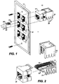
- Fig. 1 depicts a prior art wall plate 11 such as is show in the aforemetioned Arnett '442 patent. which has openings 12 therein for receiving up to six modular jacks 13.
- jack 13 comprises a jack frame 14 and a connector 16 which, together, constitute modular jack 13.
- connector 16 comprises a spring block member 17 and a cover member 18.
- Spring block 17 has a wire frame 19 mounted thereon, the leads of which curve around the nose 21 of the spring block 17 and depend at an angle therefrom to form a plurality of spring contacts 22, which mate with contact members 23 in the plug 24 when it is inserted into the opening 26 of jack frame 14 and locked by means of trigger or latching arm 25.
- the contact members 23 are each connected to an individual wire in cable 27, and the spring contacts 22 are each connected to an individual wire 28 which may be part at a cable, not shown, or which may lead to individual apparatus, not shown.
- the plug 24 and the jack 13 may form connections for a number of wires such as, for example, four or eight, depending upon the particular application.
- Wire frame 19 is shown in Fig. 2 as having eight wires, and, hence, eight spring contacts 22, which plug 24 is shown as having only four contact numbers. It is to be understood that Fig. 2 does not depict a specific connector hook-up, but is intended to illustrate the relationship of the various parts or components of the connector module. The arrangement of Figs.
- the present invention is a connector system which is intended to extend the performance range of operation but which complies with industry standards to the extent that the plug and jack of the invention an compatible with existing plugs and jacks, and which, automatically introduce capacitance into the circuitry upon sensing that either the plug or the jack is being used with a pre-existing prior art jack or plug.
- the plug and jack of the present invention exhibit "backward compatibility.”
- Fig. 3 there is shown a table depicting the industry standard allowable NEXT loss requirements at different frequencies and for different performance standard connectors, ANSI/TIA/EIA 568-A as promulgated by the Telecommunications Industry Association.
- the dB values given are, in all cases, negative values, and represent the worst-pair NEXT loss. It can be seen that the allowable loss, at 16 MHz, for a low performance connector (Category 3) is - 34 dB, whereas, for a higher performance connector (Category 5) it is - 56 dB, a much better performance figure.
- new standards are in the process of being established for even higher categories of connectors, hence the term "high performance" and it is to these connectors that the present invention is primarily directed.
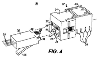
- Fig. 4 there is shown the connector assembly 31 of the present invention which comprises a jack 32 having a spring block assembly 33 and a jack frame 34, and a plug 36, connected to leads 35 of a cable or the like for use in high performance e.g . high speed data operation, but automatically adaptable for use in low performance, e.g ., low frequency analog operation.
- Both jack 32 and plug 36 are configured and wired for high performance operation in anticipation of the new parametric standardized requirements, and, as such, exhibit low crosstalk operation.
- plug 36 has mounted therein a stationary printed wiring board having a plurality of capacitance contact pads, and actuator means (not shown in Fig.
- Jack 32 also has a stationary printed wiring board 37 therein, having an actuator 38, which functions to engage a portion of a low performance plug when inserted into jack opening 26 to move the conductors into contact with the printed wiring board to introduce capacitance into wiring circuit.
- the PWBs may have more than one surface with capacitance sources thereon, or may have a layered configuration with circuit components on at least one surface thereof.
- Plug 36 has first and second recessed portions or notches 39 which are dimensioned to allow plug 36 to be inserted into opening 26 without contacting actuator 37, and jack 32 has clearance notches 41 which are dimensioned to allow the actuators for the PWB of plug 36 to pass into jack 32 without contacting the front face thereof.
- jack 32 and plug 36 from a high performance (proposed category 6 and above) connection neither PWB is caused to be introduced into the circuit, hence, no additional capacitance is introduced.
- actuators 38 will be forced toward the rear and, as will be seen hereinafter, capacitance will be introduced.
- plug 36 is inserted into a low performance jack, its actuators will move the conductors therein to the capacitance introducing position.
- both the plug 36 and the jack 32 the actuators which cause the conductors therein to contact the capacitance pads or other possible circuit elements of the stationary printed wiring boards are responsive only to the presence of a low performance jack or plug with which the plug or jack of the present invention is mated.
- mating then does not activate the actuators, each having clearances for dip actuators, hence, the conductors within the plug and the jack are not moved or depressed into contact with the PWB.
- the plug or the jack of the invention when either the plug or the jack of the invention is mated with a low performance jack or plug, neither of which has clearance for the actuators of the other components, then the low performance component activates the actuator or actuators which, in turn, depress the conductors into contact with the printed wiring board. In this manner, either the high performance plug or jack of the invention becomes a low performance component to march its mated component.
- Plug 36 comprises a substantially hollow body portion 51 having a nose or connector end 52 having a plurality of contact members 23 and a cable connection end 53 shown, for illustrative purposes only connected to three input wires 35. It is to be understood thin wires 35 an representative of a cable, or whatever member, 4, 6. 8, 12, or more of wires to be connected. As previously pointed out, the nose end 52 has first and second recessed portions 39 to allow clearance for actuators 38 of the jack 32, even when the plug 36 is fully inserted into the jack 32.
- a printed wiring board 52 i.e ., PWB, which is fixed within body 51 by suitable means, not shown.
- board 52 might be cemented in place, or fitted into channels (not shown) within body 51 and cemented.
- PWB 52 is shown as having a plurality of capacitance pads 53 arrayed as shown beneath the conductive member 23. It is to be understood that, while capacitance pads 53 (preferably gold plated) are shown, the principles of the invention are extendable to more sophisticated circuitry on PWB 52 for accomplishing other types of crosstalk reductions, for example.
- contact members are preferably in the form of blades 54, each having a distal end 56 on which are located insulation piercing teeth 57 for making electrical contact with each of the insulated wires 35.
- the blades 54 have a U-shaped configuration, as shown, to form the contacts 23, and each has an end 57 having a contact bow or bend 58.
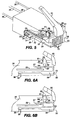
- First and second non-conducting actuating members are disposed in slots 61 in the cop of plug body 51 and project upwardly therefrom, as seen in Fig. 5.
- the bottoms 62 of buttons 59 are rounded and bear against rho tops of blades 54, and are preferably joined by a non-conducting actuating bar 63, shown in dashed lines, which bears against the tops of blades 54.
- Each button 59 has a flange 64 thereon to prevent it from extending too far out of the plug body 51. As best seen in Figs.
- FIG. 6A and 6B which depicts the high performance and low performance configurations respectively
- the resilience of blades 54 causes them to act as springs and hold the buttons in the position shown in Fig. 6A.
- the buttons 59 are cammed down by the jack, and the blades 54 are depressed so that their contact bends 58 make contact with the circuitry on PWB 52. e.g ., capacitance pads 53, as best seen in Fig. 6B, thereby converting the plug 36 to a law performance plug.
- the blades 54 spring back, producing the configuration of Fig. 6A.
- the plug 36 shown in Figs. 5, 6A, and 6B represents a preferred embodiment of the principles of the invention. It is to be understood, however, that various other configurations or structures which embody the principals of the invention might be used. For example, there is shown in Figs. 7A and 7B a variation of the arrangement of Figs. 5, 6A, and 6B, which accomplishes the same ends. For simplicity, like parts beer the same reference numerals. As can be seen in Figs. 7A and 7B, the buttons 59 of Fig. 5 have been replaced by substantially L-shaped toggles 66 which pivot with a bar or rod 67 which is pivotally mounted in the plug body 51.
- the lower limbs of the toggles 66 are joined together by an actuating bar 68 shown in dashed lines in a manner Similar to that of bar 63 in Fig. 5.
- the spring pressure of the blades form the toggles to pivot so that contact bend 58 is out of contact with PWB 52.
- the jack causes the toggles 66 to pivot so that the blades 54 are forced down so that contact bend 58 of each blade is forced into contact with the circuitry on the PWB, thus converting the plug 36 to a low performance plug.
- FIGs. 8A and 8B there is shown still another embodiment of the present invention, in which the toggles 66 and/or the buttons 59 are not necessary for operation, being replaced by an additional bend 69 in blades 54 which causes at least the blades 54 on each end of the array to extend above the top surface of plug 36, as shown in Fig. 8A.
- the plug 76 of Figs. 8A is inserted into a low performance jack, shown in dashed lines, the two end blades are forced down as shown in Fig. 8B to bring contact bends 5B into contact with PWB 52.
- the remaining blades, (designated 71 in Figs.
- a non-conducting actuating bar 72 having lobes 73 at each end which are connected to the two end blades.
- the slot 61 can be made to extend across the top wall of body 51 to insure sufficient clearance, if necessary.
- the bent portions 69 of the blades 54 are subject to exposing users to electrical voltage, as can be seen in Fig. 8B, hence an insulative coating thereon such as Mylar tape, is to be preferred.
- Fig. 9 there is shown, in an exploded perspective view, a preferred embodiment of the jack 32 of the invention, with only those components which are involved in the structure of the invention being shown, for simplicity.
- jack frame 34 but it is to be understood that other elements of the jack, which depend, at least in part, on the particular use to which it is to be put, are also to be included.
- U.S. Patent 5,096,442 of Arnett et al is incorporated herein by reference, especially for its showing of the basic components of a jack.
- jack frame 34 is substantially the same as jack frame 34 in Fig. 4 and has a front face 85 at the connector end having an opening 26 therein, configured to receive a plug. Opening 26 has a pair of clearance notches 41 which provide clearance for the actuators 59, 66, or 69 of she plug 36. Jack frame 34 is at least partially hollow, as shown, and has a rear face or portion 86. Opening 26 also has a notch 87 therein for receiving the latching member 25.
- a bar spring member 73 shown in dashed lines which extends transversely of the jack frame 34 and is affixed thereto at its ends, as shown.
- Spring contact members 22 which are mounted within the jack frame 34 by any of a number of arrangements known in the art, are the contact ends of lead frames, the other ends of which terminate in, for example, insulation displacement connector 76. It is to be understood that other types of connections than insulation displacement types, the IDCs shown in Fig. 9 being by way of example only.
- Elongated leads 77 connect the spring contact members with the IDCs 76.
- Each lead 77 has an S-shaped bend therein which comprises a first bend portion 78 and a second reverse bend portion 79, as best seen in Fig. 10, which is an inverted detail view of a portion of the apparatus of Fig. 9.
- the second bend 79 does not contact the printed wiring board 37 and the circuitry on surface 81 thereof.
- Board 37 is mounted within jack frame 34 in any suitable manner to affix it in a stationary position, oriented and located as shown in Figs. 9 and 10 so that the capacitance pads 82 (or other circuitry) directly underly bends 79 as shown in Fig. 9, or overly them, as shown in Fig. 10.
- a spacer member 83 of suitable insulating or non-conducting material is movably mounted in jack frame 34 and has, on either side thereof, spring engaging arms 84 having spring engaging hooks 88 on their distal ends.
- Actuator members 38 extend from spacer member 83 and are positioned to be engaged by a low performance plug, shown in dashed lines in Fig. 10.
- the high performance plug 36 of the invention because of the recessed portions 39 on either side thereof does not engage the actuator members 38, and actuator 83 remains stationary, held in non-PWB engaging position by bar spring member 74 which is engaged by hooks 88.
- a low performance plug When a low performance plug is inserted into jack frame 34, as shown in Fig. 10, it engages actuator members 38 and forces spacer member 83 toward the rear, causing it to press against first bend portion 78 which, in turn, causes second bend portion 79 to engage the circuitry on PWB 37, as best seen in Fig. 10.
- Spacer member 83 moves rearwardly against the force of spring member 74, and when the latching arm on the plug, designated 25 in Fig. 10, locks in place, the spring 74 is prevented from pulling spacer 83 forward into its non-engaging position. On the other hand, when the low performance plug is removed, spring 74 restores spacer 83 to its non-engaging, or high performance, position.
- the capacitance pads, or other circuitry it will be desired for the capacitance pads, or other circuitry, to be in contact with the leads 77 in the un-actuated position, to be moved out of such contact when a plug is inserted into the jack. From the foregoing it can be seen chat the principles of the invention are equally applicable to such an arrangement.
- the plug and jack of the invention automatically adapt for use, individually, with low performance jacks or plugs yet, when used together, constitute a jack performance connection.
- the jack depicted and described herein is the subject of U.S. patent application Serial Number , of Jaime R. Arnett, filed concurrently herewith (Arnett Case 60103-1720).
Landscapes
- Engineering & Computer Science (AREA)
- Signal Processing (AREA)
- Details Of Connecting Devices For Male And Female Coupling (AREA)
- Coupling Device And Connection With Printed Circuit (AREA)
Applications Claiming Priority (2)
| Application Number | Priority Date | Filing Date | Title |
|---|---|---|---|
| US292229 | 1999-04-15 | ||
| US09/292,229 US6074256A (en) | 1999-04-15 | 1999-04-15 | High performance electrical connector assembly |
Publications (3)
| Publication Number | Publication Date |
|---|---|
| EP1045490A2 true EP1045490A2 (de) | 2000-10-18 |
| EP1045490A3 EP1045490A3 (de) | 2001-03-14 |
| EP1045490B1 EP1045490B1 (de) | 2006-05-31 |
Family
ID=23123781
Family Applications (1)
| Application Number | Title | Priority Date | Filing Date |
|---|---|---|---|
| EP00303038A Expired - Lifetime EP1045490B1 (de) | 1999-04-15 | 2000-04-11 | Elektrische Verbinderanordnung mit einstellbarer Kompatibilität |
Country Status (5)
| Country | Link |
|---|---|
| US (1) | US6074256A (de) |
| EP (1) | EP1045490B1 (de) |
| JP (1) | JP3521129B2 (de) |
| AU (1) | AU759098B2 (de) |
| DE (1) | DE60028284T2 (de) |
Cited By (2)
| Publication number | Priority date | Publication date | Assignee | Title |
|---|---|---|---|---|
| DE10065595A1 (de) * | 2000-12-28 | 2002-08-14 | Ackermann Albert Gmbh Co | Elektrisches Steckverbindersystem sowie Stecker und Buchse für Steckverbindersystem |
| CN106657004A (zh) * | 2016-11-16 | 2017-05-10 | 渤海大学 | 一种内外网络物理式防攻击式转换装置 |
Families Citing this family (21)
| Publication number | Priority date | Publication date | Assignee | Title |
|---|---|---|---|---|
| US6375516B1 (en) * | 1999-02-24 | 2002-04-23 | Xircom, Inc. | RJ-45 receptacle with stops preventing insertion of RJ-11 plugs |
| US6283775B1 (en) * | 1999-08-31 | 2001-09-04 | 3Com Corporation | Electrical connector with automatic switching between multiple devices |
| DE10029649C9 (de) * | 2000-06-15 | 2008-02-07 | Adc Gmbh | Verteileranschlußmodul für die Telekommunikations- und Datentechnik |
| US6244907B1 (en) * | 2000-08-02 | 2001-06-12 | Avaya Technology Corp. | Selectable compatibility electrical connector assembly |
| US6736681B2 (en) * | 2002-10-03 | 2004-05-18 | Avaya Technology Corp. | Communications connector that operates in multiple modes for handling multiple signal types |
| CA2464834A1 (en) * | 2004-04-19 | 2005-10-19 | Nordx/Cdt Inc. | Connector |
| US7033227B2 (en) * | 2004-05-28 | 2006-04-25 | Amphenol Corporation | Modular jack receptacle |
| US7402086B2 (en) * | 2006-02-17 | 2008-07-22 | Sanbisk Il Ltd | USB connecting system and method |
| US7591686B2 (en) * | 2006-04-18 | 2009-09-22 | Commscope, Inc. Of North Carolina | Communications connectors with jackwire contacts and printed circuit boards |
| US8057246B2 (en) * | 2007-04-26 | 2011-11-15 | Tellabs Vienna, Inc. | Compact multiport test jack |
| CN101828312B (zh) * | 2007-10-08 | 2013-01-23 | 西蒙公司 | 用于监测数据端口中的连接状态的触头 |
| WO2010042586A1 (en) * | 2008-10-07 | 2010-04-15 | Molex Incorporated | Termination cap for use in wired network management system |
| US9413121B2 (en) | 2013-03-13 | 2016-08-09 | Leviton Manufacturing Co., Inc. | Communication connectors having switchable electrical performance characteristics |
| US9531135B2 (en) | 2013-03-15 | 2016-12-27 | CommScope Connectivity Spain, S.L. | Telecommunications jack with switchable circuit configurations |
| US10056703B2 (en) | 2013-07-15 | 2018-08-21 | CommScope Connectivity Spain, S.L. | Telecommunications plug for high data rate applications |
| DE102013108130A1 (de) | 2013-07-30 | 2015-02-05 | MCQ TECH GmbH | Kontaktsatz für eine Anschlussbuchse |
| US9640924B2 (en) | 2014-05-22 | 2017-05-02 | Panduit Corp. | Communication plug |
| WO2016022701A1 (en) | 2014-08-06 | 2016-02-11 | Molex Incorporated | Patch panel frame for circuit board module |
| WO2016168942A1 (en) * | 2015-04-24 | 2016-10-27 | Belden Canada Inc. | Keystone jack adaptor |
| CN110915075A (zh) * | 2017-02-10 | 2020-03-24 | 定点连接系统股份有限公司 | 以太网连接器上的开关电源 |
| US10938166B2 (en) * | 2017-02-10 | 2021-03-02 | Sentinel Connector Systems, Inc. | Switched power over ethernet connector |
Family Cites Families (14)
| Publication number | Priority date | Publication date | Assignee | Title |
|---|---|---|---|---|
| US4261633A (en) * | 1979-08-27 | 1981-04-14 | Amp Incorporated | Wiring module for telephone jack |
| US4699443A (en) * | 1984-12-28 | 1987-10-13 | American Telephone And Telegraph Company | Modular telephone jack |
| US5041018A (en) * | 1990-08-20 | 1991-08-20 | At&T Bell Laboratories | Electrical connector receptacle |
| US5096442A (en) * | 1991-07-26 | 1992-03-17 | At&T Bell Laboratories | Compact electrical connector |
| US5096439A (en) * | 1991-08-28 | 1992-03-17 | At&T Bell Laboratories | Wall plate having jack-release slots |
| US5186647A (en) * | 1992-02-24 | 1993-02-16 | At&T Bell Laboratories | High frequency electrical connector |
| DE9304405U1 (de) * | 1993-03-23 | 1993-09-02 | Albert Ackermann Gmbh & Co Kg, 51643 Gummersbach | Kodierbarer Steckverbinder |
| US5302140A (en) * | 1993-04-02 | 1994-04-12 | At&T Bell Laboratories | Connector with mounting collar for use in universal patch panel systems |
| US5346405A (en) * | 1993-05-04 | 1994-09-13 | The Whitaker Corporation | Shunted connector assembly and shunt assembly therefor |
| US5647767A (en) * | 1995-02-06 | 1997-07-15 | The Whitaker Corporation | Electrical connector jack assembly for signal transmission |
| WO1996024968A1 (en) * | 1995-02-06 | 1996-08-15 | The Whitaker Corporation | Electrical connector jack assembly for signal transmission |
| US5772466A (en) * | 1996-09-30 | 1998-06-30 | The Whitaker Corporation | Receptacle connector detecting mating with different plugs |
| US5867576A (en) * | 1996-12-13 | 1999-02-02 | Eugene A. Norden | Switching receptacle |
| EP0993082B1 (de) * | 1998-09-29 | 2003-11-12 | Nexans | Modularer Steckverbinder mit verringerter Kreuzkopplung zur Verwendung mit verschiedenen Kontaktsätzen |
-
1999
- 1999-04-15 US US09/292,229 patent/US6074256A/en not_active Expired - Lifetime
-
2000
- 2000-04-11 EP EP00303038A patent/EP1045490B1/de not_active Expired - Lifetime
- 2000-04-11 DE DE60028284T patent/DE60028284T2/de not_active Expired - Lifetime
- 2000-04-13 AU AU27740/00A patent/AU759098B2/en not_active Ceased
- 2000-04-14 JP JP2000113923A patent/JP3521129B2/ja not_active Expired - Fee Related
Cited By (2)
| Publication number | Priority date | Publication date | Assignee | Title |
|---|---|---|---|---|
| DE10065595A1 (de) * | 2000-12-28 | 2002-08-14 | Ackermann Albert Gmbh Co | Elektrisches Steckverbindersystem sowie Stecker und Buchse für Steckverbindersystem |
| CN106657004A (zh) * | 2016-11-16 | 2017-05-10 | 渤海大学 | 一种内外网络物理式防攻击式转换装置 |
Also Published As
| Publication number | Publication date |
|---|---|
| AU759098B2 (en) | 2003-04-03 |
| DE60028284D1 (de) | 2006-07-06 |
| DE60028284T2 (de) | 2007-06-06 |
| US6074256A (en) | 2000-06-13 |
| JP2001035607A (ja) | 2001-02-09 |
| EP1045490A3 (de) | 2001-03-14 |
| JP3521129B2 (ja) | 2004-04-19 |
| AU2774000A (en) | 2000-10-19 |
| EP1045490B1 (de) | 2006-05-31 |
Similar Documents
| Publication | Publication Date | Title |
|---|---|---|
| US6079996A (en) | Selectable compatibility electrical connector jack | |
| US6074256A (en) | High performance electrical connector assembly | |
| US6056568A (en) | Selectable compatibility electrical connector jack | |
| US6736681B2 (en) | Communications connector that operates in multiple modes for handling multiple signal types | |
| US6244907B1 (en) | Selectable compatibility electrical connector assembly | |
| US6059578A (en) | Selectable compatibility electrical connector assembly | |
| US6168472B1 (en) | Selectable compatibility electrical connector assembly | |
| US6109943A (en) | Selectable compatibility electrical connector plug | |
| US6139343A (en) | Selectable compatibility electrical connector plug |
Legal Events
| Date | Code | Title | Description |
|---|---|---|---|
| PUAI | Public reference made under article 153(3) epc to a published international application that has entered the european phase |
Free format text: ORIGINAL CODE: 0009012 |
|
| AK | Designated contracting states |
Kind code of ref document: A2 Designated state(s): DE FR GB |
|
| AX | Request for extension of the european patent |
Free format text: AL;LT;LV;MK;RO;SI |
|
| PUAL | Search report despatched |
Free format text: ORIGINAL CODE: 0009013 |
|
| AK | Designated contracting states |
Kind code of ref document: A3 Designated state(s): AT BE CH CY DE DK ES FI FR GB GR IE IT LI LU MC NL PT SE |
|
| AX | Request for extension of the european patent |
Free format text: AL;LT;LV;MK;RO;SI |
|
| RIC1 | Information provided on ipc code assigned before grant |
Free format text: 7H 01R 24/04 A, 7H 01R 29/00 B, 7H 01R 23/00 B, 7H 01R 13/703 B |
|
| 17P | Request for examination filed |
Effective date: 20010623 |
|
| AKX | Designation fees paid |
Free format text: DE FR GB |
|
| 17Q | First examination report despatched |
Effective date: 20021206 |
|
| GRAP | Despatch of communication of intention to grant a patent |
Free format text: ORIGINAL CODE: EPIDOSNIGR1 |
|
| RIC1 | Information provided on ipc code assigned before grant |
Ipc: 7H 01R 13/703 B Ipc: 7H 01R 29/00 B Ipc: 7H 01R 24/04 A |
|
| GRAS | Grant fee paid |
Free format text: ORIGINAL CODE: EPIDOSNIGR3 |
|
| GRAL | Information related to payment of fee for publishing/printing deleted |
Free format text: ORIGINAL CODE: EPIDOSDIGR3 |
|
| GRAS | Grant fee paid |
Free format text: ORIGINAL CODE: EPIDOSNIGR3 |
|
| GRAA | (expected) grant |
Free format text: ORIGINAL CODE: 0009210 |
|
| AK | Designated contracting states |
Kind code of ref document: B1 Designated state(s): DE FR GB |
|
| REG | Reference to a national code |
Ref country code: GB Ref legal event code: FG4D |
|
| REF | Corresponds to: |
Ref document number: 60028284 Country of ref document: DE Date of ref document: 20060706 Kind code of ref document: P |
|
| ET | Fr: translation filed | ||
| PLBE | No opposition filed within time limit |
Free format text: ORIGINAL CODE: 0009261 |
|
| STAA | Information on the status of an ep patent application or granted ep patent |
Free format text: STATUS: NO OPPOSITION FILED WITHIN TIME LIMIT |
|
| 26N | No opposition filed |
Effective date: 20070301 |
|
| PGFP | Annual fee paid to national office [announced via postgrant information from national office to epo] |
Ref country code: FR Payment date: 20100506 Year of fee payment: 11 |
|
| REG | Reference to a national code |
Ref country code: FR Ref legal event code: ST Effective date: 20111230 |
|
| PG25 | Lapsed in a contracting state [announced via postgrant information from national office to epo] |
Ref country code: FR Free format text: LAPSE BECAUSE OF NON-PAYMENT OF DUE FEES Effective date: 20110502 |
|
| PGFP | Annual fee paid to national office [announced via postgrant information from national office to epo] |
Ref country code: GB Payment date: 20130429 Year of fee payment: 14 |
|
| GBPC | Gb: european patent ceased through non-payment of renewal fee |
Effective date: 20140411 |
|
| PG25 | Lapsed in a contracting state [announced via postgrant information from national office to epo] |
Ref country code: GB Free format text: LAPSE BECAUSE OF NON-PAYMENT OF DUE FEES Effective date: 20140411 |
|
| PGFP | Annual fee paid to national office [announced via postgrant information from national office to epo] |
Ref country code: DE Payment date: 20150429 Year of fee payment: 16 |
|
| REG | Reference to a national code |
Ref country code: DE Ref legal event code: R119 Ref document number: 60028284 Country of ref document: DE |
|
| PG25 | Lapsed in a contracting state [announced via postgrant information from national office to epo] |
Ref country code: DE Free format text: LAPSE BECAUSE OF NON-PAYMENT OF DUE FEES Effective date: 20161101 |