EP1045435A2 - Chemical vapor deposition of Pb5Ge3O11 thin film for ferroelectric applications - Google Patents
Chemical vapor deposition of Pb5Ge3O11 thin film for ferroelectric applications Download PDFInfo
- Publication number
- EP1045435A2 EP1045435A2 EP00303139A EP00303139A EP1045435A2 EP 1045435 A2 EP1045435 A2 EP 1045435A2 EP 00303139 A EP00303139 A EP 00303139A EP 00303139 A EP00303139 A EP 00303139A EP 1045435 A2 EP1045435 A2 EP 1045435A2
- Authority
- EP
- European Patent Office
- Prior art keywords
- fem
- gate unit
- depositing
- junction region
- layer
- Prior art date
- Legal status (The legal status is an assumption and is not a legal conclusion. Google has not performed a legal analysis and makes no representation as to the accuracy of the status listed.)
- Withdrawn
Links
Images

Classifications
-
- H—ELECTRICITY
- H10—SEMICONDUCTOR DEVICES; ELECTRIC SOLID-STATE DEVICES NOT OTHERWISE PROVIDED FOR
- H10D—INORGANIC ELECTRIC SEMICONDUCTOR DEVICES
- H10D64/00—Electrodes of devices having potential barriers
- H10D64/60—Electrodes characterised by their materials
- H10D64/66—Electrodes having a conductor capacitively coupled to a semiconductor by an insulator, e.g. MIS electrodes
- H10D64/68—Electrodes having a conductor capacitively coupled to a semiconductor by an insulator, e.g. MIS electrodes characterised by the insulator, e.g. by the gate insulator
- H10D64/689—Electrodes having a conductor capacitively coupled to a semiconductor by an insulator, e.g. MIS electrodes characterised by the insulator, e.g. by the gate insulator having ferroelectric layers
-
- H—ELECTRICITY
- H10—SEMICONDUCTOR DEVICES; ELECTRIC SOLID-STATE DEVICES NOT OTHERWISE PROVIDED FOR
- H10P—GENERIC PROCESSES OR APPARATUS FOR THE MANUFACTURE OR TREATMENT OF DEVICES COVERED BY CLASS H10
- H10P14/00—Formation of materials, e.g. in the shape of layers or pillars
- H10P14/60—Formation of materials, e.g. in the shape of layers or pillars of insulating materials
- H10P14/69—Inorganic materials
- H10P14/692—Inorganic materials composed of oxides, glassy oxides or oxide-based glasses
- H10P14/6938—Inorganic materials composed of oxides, glassy oxides or oxide-based glasses the material containing at least one metal element, e.g. metal oxides, metal oxynitrides or metal oxycarbides
- H10P14/6939—Inorganic materials composed of oxides, glassy oxides or oxide-based glasses the material containing at least one metal element, e.g. metal oxides, metal oxynitrides or metal oxycarbides characterised by the metal
-
- C—CHEMISTRY; METALLURGY
- C23—COATING METALLIC MATERIAL; COATING MATERIAL WITH METALLIC MATERIAL; CHEMICAL SURFACE TREATMENT; DIFFUSION TREATMENT OF METALLIC MATERIAL; COATING BY VACUUM EVAPORATION, BY SPUTTERING, BY ION IMPLANTATION OR BY CHEMICAL VAPOUR DEPOSITION, IN GENERAL; INHIBITING CORROSION OF METALLIC MATERIAL OR INCRUSTATION IN GENERAL
- C23C—COATING METALLIC MATERIAL; COATING MATERIAL WITH METALLIC MATERIAL; SURFACE TREATMENT OF METALLIC MATERIAL BY DIFFUSION INTO THE SURFACE, BY CHEMICAL CONVERSION OR SUBSTITUTION; COATING BY VACUUM EVAPORATION, BY SPUTTERING, BY ION IMPLANTATION OR BY CHEMICAL VAPOUR DEPOSITION, IN GENERAL
- C23C16/00—Chemical coating by decomposition of gaseous compounds, without leaving reaction products of surface material in the coating, i.e. chemical vapour deposition [CVD] processes
- C23C16/22—Chemical coating by decomposition of gaseous compounds, without leaving reaction products of surface material in the coating, i.e. chemical vapour deposition [CVD] processes characterised by the deposition of inorganic material, other than metallic material
- C23C16/30—Deposition of compounds, mixtures or solid solutions, e.g. borides, carbides, nitrides
- C23C16/40—Oxides
-
- H—ELECTRICITY
- H10—SEMICONDUCTOR DEVICES; ELECTRIC SOLID-STATE DEVICES NOT OTHERWISE PROVIDED FOR
- H10B—ELECTRONIC MEMORY DEVICES
- H10B51/00—Ferroelectric RAM [FeRAM] devices comprising ferroelectric memory transistors
-
- H—ELECTRICITY
- H10—SEMICONDUCTOR DEVICES; ELECTRIC SOLID-STATE DEVICES NOT OTHERWISE PROVIDED FOR
- H10D—INORGANIC ELECTRIC SEMICONDUCTOR DEVICES
- H10D1/00—Resistors, capacitors or inductors
- H10D1/60—Capacitors
- H10D1/68—Capacitors having no potential barriers
- H10D1/682—Capacitors having no potential barriers having dielectrics comprising perovskite structures
-
- H—ELECTRICITY
- H10—SEMICONDUCTOR DEVICES; ELECTRIC SOLID-STATE DEVICES NOT OTHERWISE PROVIDED FOR
- H10D—INORGANIC ELECTRIC SEMICONDUCTOR DEVICES
- H10D30/00—Field-effect transistors [FET]
- H10D30/60—Insulated-gate field-effect transistors [IGFET]
- H10D30/701—IGFETs having ferroelectric gate insulators, e.g. ferroelectric FETs
-
- H—ELECTRICITY
- H10—SEMICONDUCTOR DEVICES; ELECTRIC SOLID-STATE DEVICES NOT OTHERWISE PROVIDED FOR
- H10P—GENERIC PROCESSES OR APPARATUS FOR THE MANUFACTURE OR TREATMENT OF DEVICES COVERED BY CLASS H10
- H10P14/00—Formation of materials, e.g. in the shape of layers or pillars
- H10P14/60—Formation of materials, e.g. in the shape of layers or pillars of insulating materials
- H10P14/63—Formation of materials, e.g. in the shape of layers or pillars of insulating materials characterised by the formation processes
- H10P14/6326—Deposition processes
- H10P14/6328—Deposition from the gas or vapour phase
- H10P14/6334—Deposition from the gas or vapour phase using decomposition or reaction of gaseous or vapour phase compounds, i.e. chemical vapour deposition
-
- H—ELECTRICITY
- H10—SEMICONDUCTOR DEVICES; ELECTRIC SOLID-STATE DEVICES NOT OTHERWISE PROVIDED FOR
- H10P—GENERIC PROCESSES OR APPARATUS FOR THE MANUFACTURE OR TREATMENT OF DEVICES COVERED BY CLASS H10
- H10P14/00—Formation of materials, e.g. in the shape of layers or pillars
- H10P14/60—Formation of materials, e.g. in the shape of layers or pillars of insulating materials
- H10P14/66—Formation of materials, e.g. in the shape of layers or pillars of insulating materials characterised by the type of materials
- H10P14/668—Formation of materials, e.g. in the shape of layers or pillars of insulating materials characterised by the type of materials the materials being characterised by the deposition precursor materials
-
- H—ELECTRICITY
- H10—SEMICONDUCTOR DEVICES; ELECTRIC SOLID-STATE DEVICES NOT OTHERWISE PROVIDED FOR
- H10P—GENERIC PROCESSES OR APPARATUS FOR THE MANUFACTURE OR TREATMENT OF DEVICES COVERED BY CLASS H10
- H10P14/00—Formation of materials, e.g. in the shape of layers or pillars
- H10P14/60—Formation of materials, e.g. in the shape of layers or pillars of insulating materials
- H10P14/69—Inorganic materials
- H10P14/692—Inorganic materials composed of oxides, glassy oxides or oxide-based glasses
- H10P14/6938—Inorganic materials composed of oxides, glassy oxides or oxide-based glasses the material containing at least one metal element, e.g. metal oxides, metal oxynitrides or metal oxycarbides
- H10P14/69398—Inorganic materials composed of oxides, glassy oxides or oxide-based glasses the material containing at least one metal element, e.g. metal oxides, metal oxynitrides or metal oxycarbides the material having a perovskite structure, e.g. BaTiO3
Definitions
- This application relates to ferroelectric thin films which are used in nonvolatile memories and specifically to a C-axis oriented ferroelectric used in a metal-ferroelectric-metal-silicon semi-conductor.
- Known ferroelectric random access memories are constructed with one transistor (1T) and one capacitor (1C).
- the capacitor is generally made by sandwiching a thin ferroelectric film between two conductive electrodes, which electrodes are usually made of platinum.
- the circuit configuration and the read/write sequence of this type of memory are similar to that of conventional dynamic random access memories (DRAM), except that no data refreshing is necessary in a FRAM.
- DRAM dynamic random access memories
- ferroelectric-gate-controlled field effect transistor FET
- ferroelectric-gate controlled devices have been known for some time and include devices known as metal-ferroelectric-silicon (MFS) FETs.
- FRAMs incorporating the MFS FET structure have two major advantages over the transistor-capacitor configuration: (1) The MFS FET occupies less surface area, and (2) provides a non-destructive readout (NDR). The latter feature enables a MFS FET device to be read thousands of times without switching the ferroelectric polarization. Fatigue, therefore, is not a significant concern when using MFS FET devices.
- Various forms of MFS FET structures may be constructed, such as metal ferroelectric insulators silicon (MFIS) FET, metal ferroelectric metal silicon (MFMS) FET, and metal ferroelectric metal oxide silicon (MFMOS) FET.
- MFIS metal ferroelectric insulators silicon
- MFMS metal ferroelectric metal silicon
- MFMOS metal ferroelectric metal oxide silicon
- the first problem is that it is difficult to form an acceptable crystalline ferroelectric thin film directly on silicon. Such structure is shown in U.S. Patent No. 3,832,700. Additionally, it is very difficult to have a clean interface between the ferroelectric material and the silicon. Further, there is a problem retaining an adequate charge in the ferroelectric material.
- a ferroelectric memory (FEM) structure on a gate region is shown in U.S. Patent No. 5,303,182, which emphasizes that the transfer of metal ions into the gate region is undesirable. Similar structure is shown in U.S. Patent No. 5,416,735.
- Film deposition techniques may be broadly classified as physical vapor deposition (PVD) and chemical processes.
- the chemical processes may further be broken down into chemical vapor deposition (CVD) and wet chemical processes, including sol-gel and metalorganic decomposition (MOD).
- PVD Physical vapor deposition
- PVD Physical vapor deposition
- PVD techniques include electron-beam evaporation.
- Sol-gel and MOD processes may be used, as these are simple processes, that provide molecular homogeneity, good composition control and low capital costs. However, these processes frequently result in film cracking when used for FE thin film formation because of large volume shrinkage during post deposition annealing.
- the method of the invention for forming a semiconductor structure having a ferroelectric memory (FEM) gate unit on a substrate of single crystal silicon includes: forming a silicon device area for the FEM gate unit; implanting doping impurities of a first type in the silicon device area to form a conductive channel of a first type for use as a source junction region and a drain junction region; forming a conductive channel of a second type to act as a gate junction region between the source junction region end drain junction region for the FEM gate unit on the silicon device area; depositing an FEM gate unit over the gate junction region, including depositing a lower electrode, depositing a c-axis oriented Pb 5 Ge 3 O 11 FE layer by Chemical vapor deposition (CVD), and depositing an upper electrode, wherein the FEM gate unit is sized on the gate junction region such that any edge of the FEM gate unit is a distance "D" from the edges of the source junction region and the drain junction region, where "D" is between about 50 nm and 300 n
- a ferroelectric memory (FEM) cell of the invention includes: a single-crystal silicon substrate including an active region therein; a source junction region and a drain junction region located in the active region, doped with doping impurities of a first type to form a pair of conductive channels of a first type; a gate junction region located in the active region between the source junction region and the drain junction region, doped to form a conductive channel of a second type; a FEM gate unit including a lower electrode, a c-axis oriented Pb 5 Ge 3 O 11 FE layer formed by CVD and an upper electrode; wherein the FEM gate unit is sized on the gate junction region such that any edge of the FEM gate unit is a distance "D" from the edges of the source junction region and the drain junction region, where "D" is between about 50 nm and 300 nm; an insulating layer, having an upper surface, overlying the junction regions, the FEM gate unit and the substrate; and a source electrode and a drain electrode, each
- An object of the invention is to manufacture a MFS FET device which incorporates c-axis FE material deposited by chemical vapor deposition.
- Another object of the invention is to provide a method of reliable chemical vapor deposition for making c-axis FE lead germanate thin films.
- Another object of the invention is to provide an MFS FET device which provides a non-destructive readout.
- Yet another object of the invention to provide an MFS FET device that occupies a relatively small surface area.
- a further object of the invention is to provide an MFS FET device which requires a relatively low programming voltage.
- the c-axis oriented ferroelectric memory (FEM) cell of the invention may be formed on a silicon-on-insulator (SOI or SIMOX) substrate, or, it may be formed in a bulk silicon substrate which has a p well formed therein.
- SOI silicon-on-insulator
- SIMOX silicon-on-insulator
- the initial description will concentrate on the formation of the FEM gate unit on a SIMOX substrate. It should be appreciated that in some forms of the FEM gate unit, a MOS transistor is fabricated simultaneously with the ferroelectric memory cell by conventional means which are well known to those of ordinary skill in the art. For the sake of clarity, the drawings do not depict the formation of the MOS transistor.
- FE materials were described as being suitable for the construction of FE devices.
- This disclosure focuses on c-axis oriented Pb 5 Ge 3 O 11 thin film FE material and a specific method for laying-down the thin film FE by chemical vapor deposition (CVD), which may be used to fabricate a number of varieties of Metal-Ferroelectric-Semiconductors (MFS), Metal-Ferroelectric-Metal-Semiconductors (MFMS), Metal-Ferroelectric-Insulator-Semiconductors (MFIS), and Metal-Ferroelectric-Metal-Insulator-Semiconductors (MFMIS) structures which may be used as non-volatile FE transistor memories for low voltage VLSI RAM arrays which require relatively low programming voltages.
- MFS Metal-Ferroelectric-Semiconductors
- MFMS Metal-Ferroelectric-Metal-Semiconductors
- MFIS Metal-Ferroelectric-
- the memory devices about to be described herein have a memory window of 2P r /C FE , where P r is the remnant polarization, and C FE is the ferroelectric capacitance of the FE gate unit.
- P r is the remnant polarization
- C FE is the ferroelectric capacitance of the FE gate unit.
- the memory devices need a relatively small dielectric constant in order to operate with a relatively low programming voltage, and also have a reasonably large remnant polarization for a large memory window.
- c-axis oriented Pb 5 Ge 3 O 11 thin film FE having a dielectric, constant of about 35, and a remnant polarization of about 3.5 ⁇ C/cm 2 provides the best FE material for these types of memories.
- the remnant polarization of the c-axis oriented FE is about 14X that of a non-c-axis oriented FE.
- the following descriptions disclose how the c-axis FE material is deposited by CVD to form an
- the source materials for CVD of FE thin films may be taken from the class of materials that are alkyls, alkoxides, beta-diketonates or metallocenes of the corresponding elements of lead germanate.
- the electrodes that sandwich the lead germanate film are made from noble metals, silicides, or conducting oxides.
- the FE thin film used in the preferred embodiment herein is c-axis oriented Pb 5 Ge 3 O 11 . This substance offers good stoichiometric control during CVD.
- CVD essentially involves chemical reactions of a volatile compound of a material to be deposited to produce a non-volatile solid that forms on a suitably placed substrate.
- CVD processes may be categorized as hot-wall or cold-wall processes, based on how the temperature is maintained in the reactor low-pressure or atmospheric-pressure, depending on the relationship between ambient pressure and the reactor pressure; and plasma-enhanced or photo-enhanced, depending on whether plasma or light is used to promote the CVD process.
- CVD precursors are one of the most critical steps in the successful deposition of complex oxide films, such as the FE thin films used in the method of the invention.
- Ideal precursors must have high vapor pressure at low vaporization temperatures, low decomposition temperatures, a large temperature window between the vaporization temperature and the decomposition temperature, resistance to contamination from constituents of the precursors, be stable under ambient conditions, and be non-toxic.
- several types of compounds will be used to grow Pb 5 Ge 3 O 11 thin films.
- the precursors include alkyls, alkoxides, ⁇ -diketonates, halides and hydrides, which are generally used with an oxidizing agent, such as oxygen or nitrous, to grow a Pb 5 Ge 3 O 11 thin film.
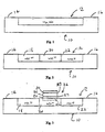
- a SIMOX substrate is depicted at 10.
- Substrate 10 in the preferred embodiment, is formed of SiO 2 , and is a single-crystal substrate.
- silicon substrate refers to either a bulk silicon substrate or a SOI substrate, or to any other suitable silicon-based substrate. As depicted in Fig.
- substrate 10 has been formed into the configuration depicted, and a portion of the substrate has been lightly doped to form an active region, or device area, 12, which provides a desired background polarity, in this case, that of an n region, which is formed by, for example, implanting phosphorous ions at an energy of between 30 keV and 120 keV, at a dose of between 1 x 10 12 cm -2 and 5 x 10 13 cm -2 .
- n region which is formed by, for example, implanting phosphorous ions at an energy of between 30 keV and 120 keV, at a dose of between 1 x 10 12 cm -2 and 5 x 10 13 cm -2 .
- a multiplicity of such regions are formed on the surface of a silicon wafer.
- the cells are arranged in a perpendicular grid to form a memory array.
- the initial description is a general method of forming and preparing the substrate that the FEM gate unit will overlay, ultimately resulting in a FEM memory cell.
- Active region 12 is bordered by non-active, or insulation regions 14, 16.
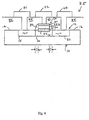
- active region 12 may be seen to have been modified to a source region 18, a gate region 20, a drain region 22. These regions are formed by applying a photoresist across active region 12 to mask what will ultimately be gate region 20, and implanting the appropriate ions in the remainder of active region 12 to form two n + layers, also referred to herein as conductive channels of a first type, which will serve as source region 18 and drain region 22.
- Appropriate ion implantation in this instance may be the implantation of arsenic ions at a preferred energy of about 50 keV, although implantation in a range of 40 keV to 70 keV is acceptable, and a dosing in a range of 2 x 10 15 cm -2 to 5 x 10 15 cm -2 .
- phosphorus ions may be implanted in an energy range of 30keV to 60 keV in the same dosing range.
- the wafer is then heat treated to activate and defuse the implanted ions. Temperature range for the heat treatment is in the range of 500 C to 1100 C.
- Gate region 20 is also referred to herein as a conductive channel of a second type. Further treatment of the substrate may occur.
- a FEM gate unit is identified generally at 24 and includes a lower electrode 26, the c-axis oriented ferroelectric (FE) material 28 and an upper electrode 30.
- the construction of FEM gate unit 24 begins with the deposition of the lower electrode on gate region 20.
- Lower electrode 26, as previously noted, should be formed of a noble metal, and may be formed of Pt or Ir, IrO 2 , an alloy of Pt/Ir, or other suitable conductive material. The thickness of this metal layer is 20 nm to 100 nm.
- the Pb 5 Ge 3 O 11 FE material is deposited by chemical vapor deposition (CVD) to a thickness of 50 nm to 400 nm.
- CVD of c-axis Pb 5 Ge 3 O 11 appears to be the best technique for forming the devices described herein, as it provides excellent film uniformity, excellent compositional control, high film density, high deposition rates, excellent step coverage, and is easily adaptable to large scale production.
- the film step coverage cannot be equalled by any other known technique.
- the film purity, controllability and precision of CVD for c-axis Pb 5 Ge 3 O 11 is competitive with much more complex and expensive molecular beam epitaxy (MBE).
- MBE molecular beam epitaxy
- Complex structures may be grown easily and precisely with CVD.
- Metalorganic CVD MOCVD is capable of producing an entire class of devices which use either ultra-thin layers or atomically sharp interfaces therein.
- CVD of Pb 5 Ge 3 O 11 requires the generation of a precursor vapor and subsequent delivery of the vapor.
- a precursor vapor such as germanium alkoxides (Ge(OC 2 H 5 ) 4 ), germanium halides (GeCl 4 , (C 2 H 5 ) 2 GeCl 2 ), lead alkyls and lead halides (Pb(C 2 H 5 ) 4 ).
- a bubbler may be used. The bubbler operates at a temperature of between 0°C and 100°C.
- a solid precursor such as lead ⁇ -diketonates (Pb(C 11 H 19 O 2 )
- the solid precursor is dissolved in a solvent, such as an aromatic hydrocarbon, cyclic hydrocarbon, or chain hydrocarbon, or a combination of the foregoing, and flash vaporized.
- a solvent such as an aromatic hydrocarbon, cyclic hydrocarbon, or chain hydrocarbon, or a combination of the foregoing, and flash vaporized.
- the solvent may be a mixture of tetrahydrofuran, iso-propanol and tetraglyme.
- Gaseous precursors such as germanium hydrides (GeH 4 , Ge x H y ), do not require special preparation.
- Delivery systems in the case of gaseous precursors, such as germanium hydrides, include an mass flow controller (MFC), and the use of carrier gases and/or vacuum systems for precursor vapors when bubblers or liquid delivery systems are used.
- MFC mass flow controller
- Lead precursor and germanium precursor vapors may be generated separately, or the source materials may be pre-mixed before the vapors are generated.
- the upper electrode 30 is then formed over the FE material.
- the upper electrode may be formed of the same materials as the lower electrode, to a thickness of 20 nm to 200 nm.
- a conductive channel precursor is identified at 32. This precursor will ultimately become a metal silicide layer 34 by diffusion of metal ion from lower electrode 26 into the gate region 20.
- a lower electrode interface 27 is located between FE layer 28 and lower electrode 26.
- An upper electrode interface 29 is located between FE layer 28 and upper electrode 30.
- Photoresist is applied over the FEM gate unit, and the cell is then etched to the proper configuration and size. It should be appreciated that the three layers of the FEM gate unit need not be precisely aligned as shown, as their shape may be formed by applying a photoresist, and etching, with masks that have different geometries. However, for the sake of clarity, the FEM gate unit is depicted as a structure which has contiguous, aligned sidewalls.
- FEM gate unit 24 is depicted as part of a FEM memory cell 35, which includes FEM gate unit 24 and the underlying source, channel and drain regions, which embodiment includes a thin layer of silicide 34 formed under FEM gate unit 24, where conductive channel precursor 32 was located.
- Silicide layer 34 may be formed prior to the deposition of the components of FEM gate unit 24, or, assuming that lower electrode 26 is formed of platinum (Pt), or an alloy thereof, the platinum may be allowed to diffuse into the upper portion of gate region 20, forming a shallow silicide layer which acts as a Schottky barrier, which is referred to herein as a conductive channel of a third type, a shallow junction, or a barrier structure.
- a layer of TiO x , 36, or other suitable barrier insulation material is formed by CVD to protect the FEM gate unit.
- the TiO x is etched to form the sidewall insulator for the gate electrode.
- Photoresist is applied and appropriate n + and p + regions are formed by ion implantation.
- An oxide layer 38 generally formed is SiO 2 , is formed by CVD, or, other suitable passivation insulation is applied.
- the structure is heat treated, at between 500 C and 1100 C, to allow passivation and diffusion of the implanted ions.
- bores are formed in oxide layer 38 and a source electrode 40, a gate electrode 42 and a drain electrode 44 are formed and connected to their respective components.
- the embodiment depicted in Fig. 4 represents the simplest case of the structure of the invention.
- the structure is a ferroelectric gate depletion-type MIS transistor.
- the charge in the n - channel underlying the FEM gate unit is completely depleted. Accordingly, the leakage current is very small.
- the distance between the point at which any edge of lower electrode 26 contacts the n silicon and the edges of the n + source or n + drain regions, represented by "D” has to be at least 50 nm in order that the leakage current remain small.
- D the series resistance of the memory cell also increases. It is therefore preferred that D be no larger than 300 nm.
- the gate leakage current is determined by the platinum to n - type silicon Schottky barrier and the platinum to c-axis oriented ferroelectric material contact.
- the gate leakage current is the gate current at a very small up to moderate field intensity.
- the potential barrier between the platinum and n - type silicon is 0.9 eV.
- a potential barrier of this magnitude causes the n - type silicon channel to be completely depleted when the c-axis oriented ferroelectric material is not polarized, or when the c-axis oriented ferroelectric material is polarized with negative charge at the lower electrode.
- the threshold voltage of the memory transistor is small. The nature of these memory charges and techniques for changing the amount of voltage necessary to the program the cells will be described later herein.
- the barrier structure serves to provide an efficient switching mechanism for the FEM cell of the invention.
- the source/drain ion implantation and annealing may be completed before the deposition of the lower gate electrode, if the ferroelectric material is unable to sustain high temperature heat treatment.
- This c-axis oriented ferroelectric memory device may be used in low voltage, high density and high speed applications.
- the memory cell is laid out on the substrate, as depicted in Fig 5.
- Fig. 5 depicts a nine-cell memory array, wherein the word lines are designated WL1, WL2 and WL3, the bit, or drain, lines are designated BL1, BL2 and BL3.
- the source regions and the substrate of all of the transistors are grounded.
- the source, word line, and bit line are connected independently to peripheral circuits, as shown in Fig 5.
- the memory array is block programmed to the "1" (high conductive) state by applying a positive voltage of V pp to the word line (gate) with the bit line connected to ground.
- V pp negative programming voltage
- the structure constructed according to the invention is particularly efficient because the FEM gate unit, located over the conductive channel on the gate region, is able to shift the polarity of the gate region, allowing efficient current flow from the source through the gate to the drain.
- the structure provides for nearly total charge depletion when in an "off” condition, and efficient, transmission of current when in an "on” condition. This is because known FEM cell configurations do not completely allow current flow through the gate region. Such structures may be thought of a switch that is partially "open.”
- Memory cells constructed according to the invention may be placed in an array of memory cells such that the gate lines run perpendicular to the drain lines, as shown in Fig. 5.
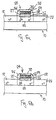
- +V P1 is applied to all gate electrodes, while the source and drain electrodes of the memory cell are at the ground potential. This polarizes the c-axis oriented FE 28 such that a positive charge is located at lower electrode interface 27 and a negative charge is located at upper electrode interface 29. (See Fig. 6a). This places FEM gate unit 24 in a high conductive state.
- the threshold voltage for FEM gate unit 24 may be determined as follows: for a large scale array the threshold voltage at the "1" state has to be a positive value, i.e., 0.4V to 0.8V. The threshold voltage for the "0" state has to be larger than the supply voltage, i.e., 3.3 V.
- V a a voltage, of no larger than the coercive voltage, i.e., that voltage where the memory content may change, is applied to the gate electrode and the drain electrode. Because the content of the memory cell is not disturbed when any electrode is biased with V a , the read operation will not disturb the memory contents of any memory cell. Therefor, a long charge retention is obtained.
- the FEM gate unit may be constructed as a single transistor device, or it may be constructed with an associated MOS transistor.
- the devices may also be configured into MFMOS, MFMS, MFIS, MIFS, MIFIS and MFS-type memories.
- the devices manufactured by the method of the invention may be used as non-volatile memory devices, capacitors, pyroelectric infrared sensors, optical displays, optical switches, piezoelectric transducers, and surface acoustic wave devices.
Landscapes
- Chemical & Material Sciences (AREA)
- Mechanical Engineering (AREA)
- General Chemical & Material Sciences (AREA)
- Chemical Kinetics & Catalysis (AREA)
- Engineering & Computer Science (AREA)
- Materials Engineering (AREA)
- Inorganic Chemistry (AREA)
- Metallurgy (AREA)
- Organic Chemistry (AREA)
- Semiconductor Memories (AREA)
- Non-Volatile Memory (AREA)
- Chemical Vapour Deposition (AREA)
- Formation Of Insulating Films (AREA)
Abstract
Description

Claims (18)
- A method of forming a semiconductor structure having a ferroelectric memory (FEM) gate unit on a substrate of single crystal silicon, comprising:forming a silicon device area for the FEM gate unit;implanting doping impurities of a first type in the silicon device area to form a conductive channel of a first type for use as a source junction region and a drain junction region;forming a conductive channel of a second type to act as a gate junction region between the source junction region and drain junction region for the FEM gate unit on the silicon device area;depositing an FEM gate unit over the gate junction region, including depositing a lower electrode, depositing a c-axis oriented Pb5Ge3O11 FE layer by Chemical vapor deposition (CVD), and depositing an upper electrode, wherein the FEM gate unit is sized on the gate junction region such that any edge of the FEM gate FEM gate unit is sized on the gate junction region such that any edge of the FEM gate unit is a distance "D" from the edges of the source junction region and the drain junction region, where "D" is between about 50 nm and 300 nm; anddepositing an insulating structure about the FEM gate unit.
- The method of claim 1 wherein source material for the c-axis Pb5Ge3O11 FE layer are taken from the group consisting of lead germanate alkyls, alkoxides, -diketonates and metallocenes.
- The method of claim 1 wherein the source material for the c-axis Pb5Ge3O11 FE layer are taken from the group consisting of Ge(OC2H5)4, GeCl4, (C2H5)GeCl2, Pb(C2H5)4, Pb(C11H19O2) and GexHy.
- The method of claim 1 wherein the c-axis Pb5Ge3O11 FE material has a dielectric constant of about 35 and a remnant polarization of bout 3.5 µC/cm2.
- The method of claim 1 wherein said depositing the FEM gate unit includes depositing the lower electrode to a thickness of about 20 nm to 100 nm, depositing the FE layer of material to a thickness of about 100 nm to 400 nm, and depositing an upper electrode to a thickness of 20 nm to 100 nm, wherein said lower electrode and said upper electrode are formed of material is taken from the group consisting of Pt, Ir, IrO2 and Pt/Ir alloy.
- The method of claim 1 wherein said implanting doping impurities of a first type includes doping the device area with ions taken from the group consisting of arsenic, implanted at an energy of about 40 keV to 70 keV, and phosphorous, implanted at an energy of about 30 keV to 60 keV, the ions having a dose of about 2 x 1015cm-2 to 5 x 1015cm-2.
- The method of claim 1 wherein said depositing an insulating structure about the FEM gate unit includes depositing a layer of insulating material taken from the group consisting of TiOx and Si3N4 over the FEM gate unit.
- The method of claim 1 which includes annealing the structure at a temperature of about 500°C to 1100°C.
- A method of forming a semiconductor structure having a ferroelectric memory (FEM) gate unit on a substrate of single crystal silicon, comprising:forming a silicon device area for the FEM gate unit;implanting doping impurities of a first type in the silicon device area to form a conductive channel of a first type for use as a source junction region and a drain junction region;forming a conductive channel of a second type to act as a gate junction region between the source junction region and drain junction region for the FEM gate unit on the silicon device area;depositing an FEM gate unit over the gate junction region, including:depositing a lower electrode;maintaining the substrate at a reduced pressure in a CVD reactor;heating the substrate in the CVD reactor,vaporizing precursors containing a lead precursor and a germanate precursor, wherein the source material for the precursors are taken from the group consisting of Ge(OC2H5)4, GeCl4, (C2H5)GeCl2, Pb(C2H5)4, Pb(C11H19O2) and GexHy;transporting vapors of the precursors into the CVD reactor;reacting the vapors in the CVD reactor;depositing a c-axis oriented Pb5Ge3O11 FE layer by chemical vapor deposition (CVD),; anddepositing an upper electrode, wherein the FEM gate unit is sized on the gate junction region such that any edge of the FEM gate unit is a distance "D" from the edges of the source junction region and the drain junction region, where "D" is between about 50 nm and 300 nm; anddepositing an insulating structure about the FEM gate unit.
- The method of claim 9 wherein the c-axis Pb5Ge3O11 FE material has a dielectric constant of about 35 and a remnant polarization of bout 3.5 µC/cm2.
- The method of claim 9 wherein said depositing the FEM gate unit includes depositing the lower electrode to a thickness of about 20 nm to 100 nm, depositing the FE layer of material to a thickness of about 100 nm to 400 nm, and depositing an upper electrode to a thickness of 20 nm to 100 nm, wherein said lower electrode and said upper electrode are formed of material is taken from the group consisting of Pt, Ir, IrO2 and Pt/Ir alloy.
- The method of claim 9 wherein said implanting doping impurities of a first type includes doping the device area with ions taken from the group consisting of arsenic, implanted at an energy of about 40 keV to 70 keV, and phosphorous, implanted at an energy of about 30 keV to 60 keV, the ions having a dose of about 2 x 1015cm-2 to 5 x 1015cm-2.
- The method of claim 9 wherein said depositing an insulating structure about the FEM gate unit includes depositing a layer of insulating material taken from the group consisting of TiOx and Si3N4 over the FEM gate unit.
- The method of claim 9 which includes annealing the structure at a temperature of about 500°C to 1100°C.
- A ferroelectric memory (FEM) cell comprising:a single-crystal silicon substrate including an active region therein;a source junction region and a drain junction region located in said active region, doped with doping impurities of a first type to form a pair of conductive channels of a first type;a gate junction region located in said active region between said source junction region and said drain junction region, doped to form a conductive channel of a second type;a FEM gate unit including a lower electrode, a c-axis oriented Pb5Ge3O11 FE layer formed by CVD and an upper electrode; wherein said FEM gate unit is sized on the gate junction region such that any edge of said FEM gate unit is a distance "D" from the edges of said source junction region and said drain junction region, where "D" is between about 50 nm and 300 nm.an insulating layer, having an upper surface, overlying said junction regions, said FEM gate unit and said substrate;a source electrode and a drain electrode, each located on the upper surface of said insulating layer and extending therethrough to make electrical contact with their respective junction regions, and a gate electrode located on the upper surface of said insulating layer and extending therethrough to make electrical contact with the upper electrode of said FEM gate unit.
- The FEM cell of claim 15 wherein said lower electrode has a thickness of about 20 nm to 100 nm, said FE layer has a thickness of about 100 nm to 400 nm, and said upper electrode has a thickness of 20 nm to 100 nm, wherein said lower electrode and said upper electrode are formed of material taken from the group consisting of Pt, Ir, IrO2 and Pt/Ir alloy.
- The FEM cell of claim 15 wherein the c-axis Pb5Ge3O11 FE material has a dielectric constant of about 35 and a remnant polarization of about 3.5 µC/cm2.
- A method of forming a c-oriented Pb5Ge3O11 layer on a substrate, comprising the steps:maintaining the substrate at a reduced pressure in a CVD reactor;heating the substrate in the CVD reactor;vaporizing precursors containing a lead precursor and a germanate precursor, wherein the source material for the precursors are taken from the group consisting of Ge(OC2H5)4, GeCl4, (C2H5)GeCl2, Pb(C2H5)4, Pb(C11H19O2) and GexHy;transporting vapors of the precursors into the CVD reactor;reacting the vapors in the CVD reactor; anddepositing a c-axis oriented Pb5Ge3O11 FE layer by chemical vapor deposition (CVD).
Applications Claiming Priority (2)
| Application Number | Priority Date | Filing Date | Title |
|---|---|---|---|
| US291688 | 1981-08-10 | ||
| US09/291,688 US6242771B1 (en) | 1998-01-02 | 1999-04-13 | Chemical vapor deposition of PB5GE3O11 thin film for ferroelectric applications |
Publications (2)
| Publication Number | Publication Date |
|---|---|
| EP1045435A2 true EP1045435A2 (en) | 2000-10-18 |
| EP1045435A3 EP1045435A3 (en) | 2002-10-30 |
Family
ID=23121396
Family Applications (1)
| Application Number | Title | Priority Date | Filing Date |
|---|---|---|---|
| EP00303139A Withdrawn EP1045435A3 (en) | 1999-04-13 | 2000-04-13 | Chemical vapor deposition of Pb5Ge3O11 thin film for ferroelectric applications |
Country Status (5)
| Country | Link |
|---|---|
| US (1) | US6242771B1 (en) |
| EP (1) | EP1045435A3 (en) |
| JP (1) | JP2000353790A (en) |
| KR (1) | KR100346563B1 (en) |
| TW (1) | TW448579B (en) |
Cited By (4)
| Publication number | Priority date | Publication date | Assignee | Title |
|---|---|---|---|---|
| WO2003052762A1 (en) * | 2001-12-14 | 2003-06-26 | Thin Film Electronics Asa | Apparatus and method for non-destructive data storage and retrieval |
| EP1391429A1 (en) * | 2002-08-06 | 2004-02-25 | Samsung Electronics Co., Ltd. | Bismuth titanium silicon oxide, bismuth titanium silicon oxide thin film, and method for forming the thin film |
| CN106709455A (en) * | 2016-12-23 | 2017-05-24 | 张帆 | Display screen for supporting full screen optical fingerprint sensor and manufacturing method thereof |
| CN108810207A (en) * | 2018-06-22 | 2018-11-13 | 昆山丘钛微电子科技有限公司 | A kind of optical finger print of screen comprehensively unlock terminal and comprehensive screen optical finger print unlocking method |
Families Citing this family (17)
| Publication number | Priority date | Publication date | Assignee | Title |
|---|---|---|---|---|
| US6303502B1 (en) * | 2000-06-06 | 2001-10-16 | Sharp Laboratories Of America, Inc. | MOCVD metal oxide for one transistor memory |
| KR100365296B1 (en) * | 2000-08-01 | 2002-12-18 | 한국과학기술연구원 | Circuit for driving non destructive non volatile ferroelectric random access memory |
| US6372034B1 (en) * | 2000-10-12 | 2002-04-16 | Sharp Laboratories Of America, Inc. | PGO solutions for the preparation of PGO thin films via spin coating |
| KR100379941B1 (en) * | 2001-03-06 | 2003-04-11 | 주승기 | Fabrication method of large single-grained ferroelectric thin film and fabrication method of ferroelectric memory device using the same |
| US6701066B2 (en) | 2001-10-11 | 2004-03-02 | Micron Technology, Inc. | Delivery of solid chemical precursors |
| US20030123080A1 (en) * | 2001-12-27 | 2003-07-03 | Toshiba Tec Kabushiki Kaisha | Image forming device and method for controling the same |
| KR100442963B1 (en) * | 2001-12-29 | 2004-08-04 | 주식회사 하이닉스반도체 | Method of manufacturing metal layer having high degree of purity |
| US7378286B2 (en) * | 2004-08-20 | 2008-05-27 | Sharp Laboratories Of America, Inc. | Semiconductive metal oxide thin film ferroelectric memory transistor |
| JP2006073939A (en) | 2004-09-06 | 2006-03-16 | Toshiba Corp | Nonvolatile semiconductor memory device and method for manufacturing nonvolatile semiconductor memory device |
| US6991942B1 (en) * | 2004-09-28 | 2006-01-31 | Sharp Laboratories Of America, Inc. | MFIS ferroelectric memory array on SOI and method of making same |
| KR101263822B1 (en) * | 2006-10-20 | 2013-05-13 | 삼성전자주식회사 | Method of manufacturing phase change memory device and method of forming phase change layer applied in the same |
| JP2008158328A (en) * | 2006-12-25 | 2008-07-10 | Ntt Docomo Inc | Terminal device and determination method |
| US20100252867A1 (en) * | 2007-10-26 | 2010-10-07 | University Of Seoul | MFMS-FET, Ferroelectric Memory Device, And Methods Of Manufacturing The Same |
| EP3062351B1 (en) * | 2013-10-22 | 2020-11-04 | National Institute of Advanced Industrial Science and Technology | Field-effect transistor |
| US9679893B2 (en) * | 2015-05-15 | 2017-06-13 | Taiwan Semiconductor Manufacturing Company Limited | Semiconductor device and transistor |
| US10374041B2 (en) * | 2017-12-21 | 2019-08-06 | International Business Machines Corporation | Field effect transistor with controllable resistance |
| US12604479B2 (en) * | 2021-09-10 | 2026-04-14 | Intel Corporation | Two transistor capacitorless memory cell with stacked thin-film transistors |
Family Cites Families (7)
| Publication number | Priority date | Publication date | Assignee | Title |
|---|---|---|---|---|
| US3832700A (en) | 1973-04-24 | 1974-08-27 | Westinghouse Electric Corp | Ferroelectric memory device |
| US5204314A (en) | 1990-07-06 | 1993-04-20 | Advanced Technology Materials, Inc. | Method for delivering an involatile reagent in vapor form to a CVD reactor |
| JP2723386B2 (en) | 1991-07-02 | 1998-03-09 | シャープ株式会社 | Non-volatile random access memory |
| US5303182A (en) | 1991-11-08 | 1994-04-12 | Rohm Co., Ltd. | Nonvolatile semiconductor memory utilizing a ferroelectric film |
| US5731608A (en) * | 1997-03-07 | 1998-03-24 | Sharp Microelectronics Technology, Inc. | One transistor ferroelectric memory cell and method of making the same |
| JP4080050B2 (en) * | 1997-03-07 | 2008-04-23 | シャープ株式会社 | Ferroelectric memory cell, semiconductor structure and manufacturing method thereof |
| US6011285A (en) * | 1998-01-02 | 2000-01-04 | Sharp Laboratories Of America, Inc. | C-axis oriented thin film ferroelectric transistor memory cell and method of making the same |
-
1999
- 1999-04-13 US US09/291,688 patent/US6242771B1/en not_active Expired - Fee Related
-
2000
- 2000-04-12 KR KR1020000019277A patent/KR100346563B1/en not_active Expired - Fee Related
- 2000-04-12 JP JP2000111300A patent/JP2000353790A/en active Pending
- 2000-04-13 TW TW089106891A patent/TW448579B/en not_active IP Right Cessation
- 2000-04-13 EP EP00303139A patent/EP1045435A3/en not_active Withdrawn
Cited By (9)
| Publication number | Priority date | Publication date | Assignee | Title |
|---|---|---|---|---|
| WO2003052762A1 (en) * | 2001-12-14 | 2003-06-26 | Thin Film Electronics Asa | Apparatus and method for non-destructive data storage and retrieval |
| RU2271581C2 (en) * | 2001-12-14 | 2006-03-10 | Тин Филм Электроникс Аса | Method for non-destructive storage and extraction of data and device for realization of said method |
| EP1391429A1 (en) * | 2002-08-06 | 2004-02-25 | Samsung Electronics Co., Ltd. | Bismuth titanium silicon oxide, bismuth titanium silicon oxide thin film, and method for forming the thin film |
| US6919597B2 (en) | 2002-08-06 | 2005-07-19 | Samsung Electronics Co., Ltd. | Bismuth titanium silicon oxide, bismuth titanium silicon oxide thin film, and method for forming the thin film |
| US7374994B2 (en) | 2002-08-06 | 2008-05-20 | Samsung Electronics Co., Ltd. | Bismuth titanium silicon oxide, bismuth titanium silicon oxide thin film, and method for forming the thin film |
| US7892917B2 (en) | 2002-08-06 | 2011-02-22 | Samsung Electronics Co., Ltd. | Method for forming bismuth titanium silicon oxide thin film |
| CN106709455A (en) * | 2016-12-23 | 2017-05-24 | 张帆 | Display screen for supporting full screen optical fingerprint sensor and manufacturing method thereof |
| CN106709455B (en) * | 2016-12-23 | 2020-06-30 | 张一帆 | A display screen supporting full-screen optical fingerprint sensor and manufacturing method thereof |
| CN108810207A (en) * | 2018-06-22 | 2018-11-13 | 昆山丘钛微电子科技有限公司 | A kind of optical finger print of screen comprehensively unlock terminal and comprehensive screen optical finger print unlocking method |
Also Published As
| Publication number | Publication date |
|---|---|
| TW448579B (en) | 2001-08-01 |
| EP1045435A3 (en) | 2002-10-30 |
| US6242771B1 (en) | 2001-06-05 |
| KR20000071669A (en) | 2000-11-25 |
| KR100346563B1 (en) | 2002-07-27 |
| JP2000353790A (en) | 2000-12-19 |
Similar Documents
| Publication | Publication Date | Title |
|---|---|---|
| US6242771B1 (en) | Chemical vapor deposition of PB5GE3O11 thin film for ferroelectric applications | |
| US5731608A (en) | One transistor ferroelectric memory cell and method of making the same | |
| US6011285A (en) | C-axis oriented thin film ferroelectric transistor memory cell and method of making the same | |
| US11398263B2 (en) | Semiconductor structures, memory cells and devices comprising ferroelectric materials, systems including same, and related methods | |
| US6117691A (en) | Method of making a single transistor ferroelectric memory cell with asymmetrical ferroelectric polarization | |
| US5146299A (en) | Ferroelectric thin film material, method of deposition, and devices using same | |
| KR950000156B1 (en) | Semiconductor devices | |
| KR940006708B1 (en) | Manufacturing method of semiconductor device | |
| EP0869557B1 (en) | Ferroelectric memory cell and method of making the same | |
| JPH08264669A (en) | Ferroelectric memory device and manufacturing method thereof | |
| US6048738A (en) | Method of making ferroelectric memory cell for VLSI RAM array | |
| US6146904A (en) | Method of making a two transistor ferroelectric memory cell | |
| EP0487739A1 (en) | Semiconductor device and a method of manufacturing such a semiconductor device | |
| US6537830B1 (en) | Method of making ferroelectric FET with polycrystalline crystallographically oriented ferroelectric material | |
| US7227210B2 (en) | Ferroelectric memory transistor with highly-oriented film on gate insulator | |
| US6960801B2 (en) | High density single transistor ferroelectric non-volatile memory | |
| KR102433698B1 (en) | A method used to form at least a portion of at least one conductive capacitor electrode of a capacitor comprising a pair of conductive capacitor electrodes having a capacitor insulator therebetween, and a method of forming a capacitor. | |
| US5955755A (en) | Semiconductor storage device and method for manufacturing the same | |
| US6291292B1 (en) | Method for fabricating a semiconductor memory device | |
| US5942776A (en) | Shallow junction ferroelectric memory cell and method of making the same | |
| US20040051126A1 (en) | Compositionally engineered CexMnyO3 and semiconductor devices based thereon | |
| US6018171A (en) | Shallow junction ferroelectric memory cell having a laterally extending p-n junction and method of making the same | |
| JPH07273232A (en) | Semiconductor device and manufacturing method thereof | |
| US20020108927A1 (en) | Method of fabricating ferroelectric memory transistors | |
| KR100219522B1 (en) | A semiconductor device having single crystal ferroelectric film and fabrication method of the same |
Legal Events
| Date | Code | Title | Description |
|---|---|---|---|
| PUAI | Public reference made under article 153(3) epc to a published international application that has entered the european phase |
Free format text: ORIGINAL CODE: 0009012 |
|
| AK | Designated contracting states |
Kind code of ref document: A2 Designated state(s): AT BE CH CY DE DK ES FI FR GB GR IE IT LI LU MC NL PT SE |
|
| AX | Request for extension of the european patent |
Free format text: AL;LT;LV;MK;RO;SI |
|
| PUAL | Search report despatched |
Free format text: ORIGINAL CODE: 0009013 |
|
| AK | Designated contracting states |
Kind code of ref document: A3 Designated state(s): AT BE CH CY DE DK ES FI FR GB GR IE IT LI LU MC NL PT SE |
|
| AX | Request for extension of the european patent |
Free format text: AL;LT;LV;MK;RO;SI |
|
| RIC1 | Information provided on ipc code assigned before grant |
Free format text: 7H 01L 21/336 A, 7H 01L 21/28 B, 7H 01L 29/78 B, 7H 01L 29/51 B |
|
| 17P | Request for examination filed |
Effective date: 20030128 |
|
| AKX | Designation fees paid |
Designated state(s): DE FR GB |
|
| 17Q | First examination report despatched |
Effective date: 20070202 |
|
| STAA | Information on the status of an ep patent application or granted ep patent |
Free format text: STATUS: THE APPLICATION IS DEEMED TO BE WITHDRAWN |
|
| 18D | Application deemed to be withdrawn |
Effective date: 20100327 |