-
The present invention relates generally to lithography systems for
semiconductor fabrication, and more specifically to reducing carbon contamination in
sub-atmospheric charged particle beam lithography systems.
-
Photolithography has become a critical enabling technology in the fabrication
of modern integrated circuit (IC) devices. The photolithography process typically
involves exposing a patterned mask to collimated radiation to produce patterned
radiation. The patterned radiation is then passed through an optical reduction system,
and the reduced patterned radiation or mask image is projected onto a substrate,
typically a silicon wafer, that is coated with photoresist. The radiation exposure
changes the properties of the photoresist and allows subsequent processing of the
substrate.
-
As the degree of circuit integration has increased, the feature sizes of IC's
have dramatically decreased. To support future semiconductor fabrication
requirements, lithography systems using charged particle beams, such as electron
beams or ion beams, have been developed to overcome limitations of traditional
optical systems. In charged particle beam projection lithography systems, portions of
a mask are illuminated with a charged particle beam to project an image of the mask
onto a substrate. Several new charged particle beam lithography systems have been
developed to extend lithography capabilities to sub-0.15 micron feature size levels.
One such system is a microcolumn electron beam system developed by IBM. This
system uses a large number of miniature electron beam writers in a phased array to
project mask images on the order of 0.1 micron wafer geometries. Another such
system is a SCALPEL® electron beam lithography system developed by AT&T Bell
Laboratories; SCALPEL, stands for "Scattering with Angular Limitation in Projection
Electron-beam Lithography" and is a registered trademark of AT&T Bell Laboratories
of Murray Hill, New Jersey. The SCALPEL lithography system projects high-energy
electrons through a photomask.
-
A significant disadvantage associated with current, charged particle beam
lithography systems is a susceptibility to carbon contamination on the mask, walls,
and other surfaces of the imaging (or process) chamber of the lithography system.
Repeated exposure of a mask to charged particle beams tends to cause a build-up of
carbon on the mask if sufficiently high enough levels of carbon contaminants are
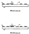
present in the imaging chamber. Figure 1A illustrates a side view of a mask, such as a
mask used in a SCALPEL lithography system. The mask has an image pattern
formed on it and is used to project a reduced image pattern onto a substrate. The
critical dimension (CD) represents the smallest feature size or spacing between
features routinely produced on the substrate forming the integrated circuit device.
The CD is controlled by feature 102 on mask 100 which has a dimension 104, and
which produces the CD on the wafer. For a mask used in the SCALPEL lithography
system, feature 102 represents a "blocking" region and surface 106 represents a
transparent region. A blocking region scatters incident electrons and a transparent
region transmits incident electrons.
-
Carbon deposits on the mask or on the wafer may cause the CD to change
(usually to increase). This effect is illustrated in Figure 1B, in which carbon deposit
112 on feature 102 has increased the dimension of feature 102 from a first width 104
to a second width 114. Carbon deposits on the features of the mask can also cause
heating of the mask features due to excessive absorption, rather than scattering, of
incident electrons. Such heating can cause the mask features to become undesirably
distorted.
-
Even in cases in which the degree of carbon deposition on the mask is not
significant enough to alter the CD, the presence of contaminants on the mask and
aperture surfaces can cause unwanted deflection of an electron beam which passes
through the mask and/or other apertures. With reference to Figure 1B, carbon deposit
116 on the transparent region of the mask 100 can cause incident electrons to be
undesirably scattered and thereby produce an unwanted image on the wafer. Thus,
even minute amounts of carbon contamination can adversely affect the imaging
process within electron beam lithography systems.
-
Carbon contamination can be introduced by various sources into the imaging
chamber that contains the electron source, mask, wafer, and imaging components of a
charged particle beam lithography system. These sources of contamination include
hydrocarbon vapor that might be present in the chambers or carbon residue in the
wiring or electron sources, stage supports, and other similar sources. While it is
possible to reduce carbon contamination by ensuring that exclusively non-carbon
materials are used in the imaging chamber, or by physically cleaning the chamber and
mask often and thoroughly, such measures are typically very expensive and time
consuming, and limit the throughput of the lithography system. Moreover, such
methods may not totally remove the carbon contamination in the imaging chamber,
since organic compounds are often present in the masks and wafers themselves.
-
In light of the above, there is a need in the art for a system for the removal of
carbon contamination deposited within the chambers of an electron beam
photolithography apparatus.
-
The present invention relates to a cleaning system that prevents build-up of
carbon deposits in an imaging chamber of a sub-atmospheric charged particle beam
lithography system. In particular, the invention relates to a cleaning system that
eliminates built-up carbon deposits on mask and imaging chamber surfaces in the sub-atmospheric
charged particle beam lithography system.
-
A cleaning system for use with a sub-atmospheric charged particle beam
lithography system is described. In one embodiment of the present invention, the
cleaning system includes an oxidizer source that introduces an oxidizer into an
imaging chamber of the lithography system to oxidize carbon contamination that has
built up on the surfaces within the chamber, such as the mask and chamber walls. A
volatile gas species comprising oxidized carbon gas is produced from the oxidization
process. This volatile gas is pumped out of the chamber by a vacuum pump coupled
to the imaging chamber, to thereby remove the carbon contaminant deposits from the
imaging chamber.
-
In one embodiment of the present invention, a cleaning process comprises
evenly directing an oxidizer, such as oxygen gas, across the mask to remove carbon
deposits from the mask while the mask is situated in the imaging chamber and the
chamber is maintained at a sub-atmospheric pressure. In accordance with this
embodiment of the present invention, the cleaning process is performed periodically
after a predetermined number of wafers have been processed. In an alternative
embodiment of the present invention, the cleaning process is performed continuously
by introducing an oxidizer into the imaging chamber while each wafer is being
processed.
-
The present invention is illustrated by way of example and not limitation in
the figures of the accompanying drawings, in which like references indicate similar
elements, and in which:
- Figure 1A is a side view of a mask;
- Figure 1B is a side view of the mask of Figure 1A illustrating the effect of
carbon deposits on the mask;
- Figure 2A illustrates an oxygen-based cleaning system for a sub-atmospheric
electron beam lithography system, according to one embodiment of the present
invention;
- Figure 2B illustrates an oxygen-based cleaning system for a sub-atmospheric
electron beam lithography system, according to an alternative embodiment of the
present invention;
- Figure 2C illustrates an oxygen-based cleaning system for a sub-atmospheric
electron beam lithography system, according to a further alternative embodiment of
the present invention;
- Figure 3 is a more detailed diagram of the electron beam lithography system
illustrated in Figure 2A;
- Figure 4 is a flowchart that illustrates the steps of cleaning carbon deposits
from an imaging chamber of a sub-atmospheric charged particle beam lithography
system, according to one embodiment of the present invention; and
- Figure 5 illustrates a mask protection system that can be used in conjunction
with embodiments of the present invention.
-
-
A cleaning system for a sub-atmospheric charged particle beam lithography
system is described. In the following description, for purposes of explanation,
numerous specific details are set forth in order to provide a thorough understanding of
the present invention. It will be evident, however, to one of ordinary skill in the art,
that the present invention may be practiced without these specific details. In other
instances, well-known structures and devices are shown in block diagram form to
facilitate explanation. The description of preferred embodiments is not intended to
limit the scope of the claims appended hereto.
-
During charged particle beam lithography, high energy charged particle beams
are projected through a mask to project an image of portions of the mask onto a
substrate, such as a silicon wafer. Typical charged particle beam lithography systems
use electron beam or ion beam projection systems to fabricate a wafer using an image
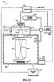
mask. Figure 2A is a cross sectional illustration of an electron beam lithography
system 200 for use in semiconductor processing, and that implements embodiments of
the present invention.
-
In one embodiment of the present invention, a carbon deposit cleaning system
is implemented in a SCALPEL (Scattering with Angular Limitation in Projection
Electron-beam Lithography) system. Figure 2A is a cross sectional illustration of a
basic SCALPEL system that has been modified for use with embodiments of the
present invention.
-
As is well known, in a SCALPEL system, high-energy electrons are projected
through a mask to project an image of the mask onto the substrate. The mask
generally consists of a low atomic number membrane covered with a layer of a high
atomic number material. The mask pattern is formed in the high atomic number
material as a pattern layer. The mask is nearly transparent to electron at the energies
used to transmit the electrons (typically 100 keV); however, the difference in electron
scattering characteristics between the low atomic number membrane and high atomic
number patterned layer provides sufficient contrast to project an image onto the
wafer. The electrons transmitted through the membrane are substantially unscattered
and the electrons transmitted through the pattern layer are scattered. The SCALPEL
system includes an aperture in the back-focal plane of the projection optics that blocks
the strongly scattered electrons. This forms a high contrast image at the wafer plane.
-
With reference to Figure 2A, system 200 represents a SCALPEL lithography
system that includes embodiments of the present invention. The lithography system
includes an electron source 202, which is typically implemented as an electron gun.
Electron source 202 projects beams of electrons in the form of a high density electron
flux 203 through an illumination column in an illumination chamber 204 to mask
stage 206. Mask stage 206 holds a mask 208 that includes an electron transparent
membrane layer and a pattern layer. The electron beams pass through the mask 208
and an imaging (or projection) column 210 to form focused electron beams 205 that
are projected onto a wafer 214 held by wafer stage 212. Imaging column 210 also
includes a back-focal plane aperture (shown as element 312 in Figure 3) that blocks
scattered electrons and allows unscattered electrons to pass through to the wafer 214.
-
The mask stage 206, wafer stage 212, and imaging column 210 are enclosed
within a process chamber 220. For a SCALPEL system, the process chamber 220 is
generally maintained at a sub-atmospheric environment, and thus may also be referred
to as a vacuum chamber. The mask stage 206 and wafer stage 212 are generally
mounted to the top and bottom of a large metal block referred to as a metrology plate
(not shown to avoid unnecessarily obscuring the illustration) that serves as a thermal
and mechanical stabilizer for the entire optical system. A vacuum pump 218 is
coupled to the process chamber 220 to create a vacuum within chamber 220 during
the imaging process. As stated above, during wafer fabrication, the process chamber
220 is maintained at a sub-atmospheric (vacuum or partial vacuum) state. For a
typical SCALPEL system, the process chamber is generally maintained under a
vacuum of 10-6 to 10-7 Torr, while the illumination chamber maintained under a
vacuum of 10-8 to 10-9 Torr.
-
At such low pressures, gas molecules generally follow their initial trajectory
until they strike the walls. Any carbon that is present will likely stick to the walls,
thus creating carbon contamination within the chambers. However, oxidizing the
carbon creates an oxidized carbon gas (CO or CO2) that exhibits a relatively low
sticking coefficient. This gas can then be effectively removed from the illumination
and/or process chamber with the vacuum pump.
-
Also coupled to the imaging chamber 220 are one or more air locks 217 that
allow the exchange of wafers to and from the process chamber 220, without breaking
the vacuum within the process chamber 220 during wafer fabrication. For this
embodiment, illumination chamber 204 and process chamber 220 together comprise
an imaging chamber for system 200. Thus, unless otherwise indicated, for the
embodiment illustrated in Figure 2A, the term 'imaging chamber' as used herein
includes both illumination chamber 204 and process chamber 220. For this
embodiment, mask stage 206 and mask 208 do not form an airtight barrier between
the two chambers 204 and 220. It should be noted that for other embodiments of the
present invention, the imaging chamber may refer to either the illumination chamber
or the process chamber alone, as opposed to both chambers together.
-
In one embodiment of the present invention, mask 208 is mounted within or
attached to a support ring (not shown to avoid unnecessarily obscuring the
illustration) that is coupled to mask stage 206. For this embodiment, mask stage 206
includes an opening that allows electrons to pass through the mask 208, and also
allows gas to flow over the surface of mask 208. Depending on the lithography
system used, other mask support structures are also possible.
-
A problem associated with present SCALPEL lithography systems, and other
charged particle beam projection lithography systems, is the possibility of carbon
build-up on the mask, wafer, and/or other surfaces within the imaging chamber during
the lithography process. The presence of carbon contamination, either in the form of
hydrocarbon vapor in the imaging chamber or organic materials on surfaces within the
chamber (e.g., wires, walls, and so on) can cause carbon deposition on the mask or
wafer during chamber operation. These carbon deposits can negatively impact the
imaging effectiveness of the system by undesirably scattering an electron beam, or by
increasing the feature size of the mask image, as illustrated in Figures 1A and 1B.
Although it is possible to minimize such carbon contamination in the imaging
chamber, it is not always possible or cost-efficient to maintain a carbon-free system,
since carbon can be easily introduced by many different sources. For example,
continuous exposure of the wafer to electron-beam processing causes a release of
carbon through the outgassing from the wafer and the presence of organic materials in
the wafer.
-
In one embodiment of the present invention shown in Figure 2A, lithography
system 200 includes an oxidizer source 216 that introduces an oxidizer into
illumination chamber 204 and process chamber 220 (together, the imaging chamber)
at a predetermined pressure and rate of flow. The oxidizer provided by oxidizer
source 216 is typically in the form of pure oxygen gas. In an alternative embodiment
of the present invention, the oxidizer may be sourced from any oxygen containing
compound, such as O3, N2O, water vapor, doped oxygen compounds, alcohol
compounds, and other like compounds that are either neutral or ionized. In a further
alternative embodiment of the present invention, the oxidizer may be any gaseous
compound that can be introduced into the imaging chamber and that acts to oxidize
any resident carbon into a volatile gas species. The selection of the oxidizer must be
made keeping in mind that the oxidizer should not corrode or damage other
components of the lithography system.
-
In one embodiment of the present invention, the oxidizer provided by oxidizer
source 216 is in an activated state. The oxidizer is activated by one of several
different possible methods, including thermal activation, ozone activation, activation
by a microwave source or remote plasma source, or other similar methods. For this
embodiment, oxidizer source 216 includes microwave circuitry to activate the
oxidizer, or other circuitry that is appropriate for the oxidizer activation method.
-
In one embodiment of the present invention, oxidizer is introduced at specified
flow rates until particular partial pressures within the illumination chamber 204 and
process chamber 220 are reached. For high-pressure applications, such as those in
which a large diameter wafer 214 is processed or in a system that is subject to heavy
carbon build-up, oxidizer is pumped into the imaging chamber from oxidizer source
216 through a high pressure pump. A flow control unit 219 controls the flow of
oxidizer into the imaging chamber. The flow control unit 219 allows a user to
independently specify and monitor the flow of oxidizer to the illumination chamber
204 and process chamber 220, on a precise basis. The actual oxidizer flow rates and
pressures that are maintained depends on several factors, including the size of the
mask 208, the volume of the illumination chamber 204, the volume of the process
chamber 220, and the amount of carbon contamination that is to be removed. For a
sub-atmospheric lithography system, oxidizer is introduced at a rate and pressure that
maintains the sub-atmospheric environment within the imaging chamber.
-
In one embodiment of the present invention a computer 222 is used to control
the vacuum pump 218, electron source 202, flow control unit 219 and one or more air
locks 217. The computer 222 can automatically control the cleaning process by
coordinating the operation of the lithography system 200 components. The computer
222 also allows the lithography system 200 components to be manually controlled by
an operator through a user input. The user input may also be connected to other
control systems that can coordinate the operation of the lithography system 200 with
other connected wafer processing components, including a wafer transportation
system or a cluster tool.
-
For the embodiment of the present invention illustrated in Figure 2A, oxidizer
is introduced into illumination chamber 204 through a nozzle 224 inserted through a
wall of the illumination chamber 204, and into process chamber 220 through a nozzle
215 that is inserted through a wall of the process chamber 220. Since carbon
contamination on the mask itself is typically the most critical in a SCALPEL system,
the nozzle 215 is configured to evenly direct the oxidizer flow across a surface of the
mask 208. Alternatively, however, the nozzles 215 and 224 may be aimed or
configured to direct oxidizer over other surfaces in the illumination chamber 204 and
process chamber 220 such as the walls or the wafer area. This allows the oxidizer to
be concentrated at the regions in which removal of carbon build-up is most desired.
The diameter of nozzles 215 and 224, and the extent to which they extend into the
illumination chamber 204 and process chamber 220 can be adjusted depending on the
requirements of the cleaning system and the physical and operational constraints of
the lithography system 200.
-
Although the embodiment illustrated in Figure 2A shows the introduction of
the oxidizer into the illumination chamber 204 and process chamber 220 by means of
nozzles 215 and 224, it is to be noted that the oxidizer can be introduced into the
imaging chamber in a number of different ways. For example, in alternative
embodiments of the present invention, the oxidizer can introduced into the imaging
chamber through a gas injection manifold or a shaped tube with air inlet holes, that
distribute the oxidizer generally into the imaging chamber and across the surface of
the mask 208.
-
Figure 2B illustrates an electron beam lithography system that implements a
cleaning system according to an alternative embodiment of the present invention. For
this embodiment, the oxidizer supplied by oxidizer source 216 is pumped into
illumination chamber 204 through gas injection manifold 221. Gas injection manifold
221 includes a plurality of inlet holes 223 to direct the oxidizer into the illumination
chamber 204. The gas injection manifold 221 is positioned within the illumination
chamber 204 such that the inlet holes 223 are distributed around the inside surface of
the illumination chamber 204 and are substantially flush with the inside surface of the
illumination chamber 204. Thus, in Figure 2B, which illustrates a cross-sectional
view of the electron-beam lithography system 250, gas injection manifold 221 runs
continuously along the inside surface of the illumination chamber 204.
-
In one embodiment of system 250 illustrated in Figure 2B, gas injection
manifold 221 is a hollow chamber that distributes the oxidizer supplied by oxidizer
source 216 through each of the inlet holes 223. Alternatively, gas injection manifold
221 may include individual nozzles coupled to each of the inlet passages 223 to direct
the oxidizer into the illumination chamber 204 in a specific direction or pattern. As
illustrated in Figure 2B, the configuration and location of the gas injection manifold
221 and the inlet holes 223 within the gas injection manifold 221 are arranged to
direct the flow of the oxidizer evenly across the surface of mask 208. However, it
should be noted that the configuration and location of the inlet holes 223 and gas
injection manifold 221 within the illumination chamber 204 can be varied from the
configuration illustrated in Figure 2B to provide different oxidizer flow patterns with
the illumination chamber 204. The configuration and operation of the other
components illustrated in Figure 2B corresponds to the description provided above
with reference to Figure 2A.
-
For the embodiment illustrated in Figure 2B, oxidizer may also be introduced
into the imaging chamber by a nozzle 215 inserted into the process chamber 220.
Alternatively, in system 250, oxidizer is introduced into the imaging chamber only
through gas injection manifold 221.
-
A further alternative embodiment of the present invention that implements a
cleaning system for an electron beam lithography system is illustrated in Figure 2C.
In system 270 of Figure 2C, the oxidizer is introduced into illumination chamber 204
through a circular inlet tube 233 that is proximately located round the mask 208. In
one embodiment of the system 270 illustrated in Figure 2C, inlet tube 233 is a hollow
cylindrical tube that is formed into a continuous circular passage. The circular inlet
tube 233 contains a plurality of holes 239 distributed around its surface. The circular
inlet tube 233 is supported by one or more braces, such as brace 237, that are attached
to the walls of illumination chamber 204. Oxidizer source 216 provides the oxidizer
through passage 235 to circular inlet tube 233 and the oxidizer flows through the inlet
tube and exits from the holes 239. In this manner, the oxidizer flows uniformly and
directly across the surface of mask 208. It should be noted that the shape, size, and
orientation of circular inlet tube 233 can be modified as required to direct the oxidizer
across specific surfaces of the mask 208 or illumination chamber 204, or to
concentrate the oxidizer flow across particular portions of the mask 208 or
illumination chamber 204 surfaces. Because the inlet tube in system 270 is located in
relatively close proximity to the mask 208, the embodiment illustrated in Figure 2C
generally provides a more concentrated and uniform flow of the oxidizer across the
surface of the mask 208 than the embodiment illustrated in Figure 2B. The
configuration and operation of the other components illustrated in Figure 2C
correspond to the description provided above with reference to Figure 2A.
-
For the embodiment illustrated in Figure 2C, oxidizer may also be introduced
into the imaging chamber by a nozzle 215 inserted into the process chamber 220.
Alternatively, in system 270, oxidizer is introduced into the imaging chamber only
through circular inlet tube 223.
-
It should be noted that other oxidizer introduction schemes in accordance with
embodiments of the present invention are also possible. For example, in another
alternative embodiment of the present invention, the oxidizer is introduced directly
onto the surface of the mask, without being introduced into the imaging chamber. For
this embodiment, one or more inlet passages are provided in the mask stage 206 to
direct the oxidizer from the oxidizer source directly onto the mask 208.
-
In one embodiment of the present invention, the oxidizer that is introduced
into the imaging chamber from the oxidizer source acts to oxidize any carbon
contaminants that may be present within the chamber. Thus, any carbon residue or
deposits on the mask and walls of the chamber, and on any other surface within the
chamber is oxidized. The oxidization process transforms any carbon residue that is in
solid form to a gaseous form. Likewise, any hydrocarbon gas that is present in the
imaging chamber is oxidized by the oxidizer that is supplied by the oxidizer source.
The oxidization process thus creates an oxidized carbon gas within the imaging
chamber. Such a gas may be produced in the form of carbon monoxide (CO) or
carbon dioxide (CO2), or other volatile carbon-oxygen compounds. The oxidized
carbon gas is a volatile gas species that can be evacuated from the imaging chamber
to thereby remove the oxidized carbon contaminants.
-
In one embodiment of the present invention, the oxidizer is introduced into the
imaging chamber for a period of time that is sufficient to thoroughly expose the mask
or other desired surfaces to the oxidizer. The period of time generally depends upon
the volume of the chamber, the amount of carbon build-up, and the sensitivity of
wafer and mask features to oxidization. After the carbon deposits and residue have
been oxidized, the resulting oxidized carbon gas is pumped out of the imaging
chamber. In this manner, the carbon contamination within the imaging chamber is
removed from the mask and/or chamber surfaces.
-
In one embodiment of the present invention, the oxidizer is introduced into the
imaging chamber during the wafer fabrication process. For this embodiment, the
mask is cleaned while the imaging chamber is maintained in a sub-atmospheric
(partial vacuum) environment. As the oxidizer is directed across the mask, carbon
deposits on the mask are oxidized. The resulting oxidized carbon gas is then pumped
out of the imaging chamber by the operation of a vacuum pump.
-
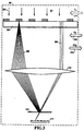
A more detailed illustration of the beam path in the imaging chamber of a
particle beam lithography system is illustrated in Figure 3. Figure 3 illustrates typical
charged particle beam paths for the SCALPEL lithography system illustrated in
Figure 2A. In Figure 3, an electron flux 302 comprising a plurality of electron beams
is projected through mask 304. In accordance with a SCALPEL lithography system,
electron beams that strike the pattern layer of the mask 304 scatter, as illustrated by
the scattered beams 306; while electron beams travel unscattered through the
membrane, as illustrated by the unscattered beams 308. The unscattered electron
beams 308 are focused by electron lens 310, illustrated as an optional lens for ease of
understanding the present invention, and pass through a back-focal plane aperture 312
and impinge upon the wafer 314. The scattered beams 306 are redirected by electron
lens 310 but are effectively blocked by aperture 312. During the imaging process for
a SCALPEL system, the imaging chamber 301 is maintained at a sub-atmospheric
pressure.
-
In one embodiment of the present invention, one or more oxidizer streams 316
and 320 we directed across the surface of the mask 304. Carbon deposits on the mask
304, as well as on other surfaces of the chamber 301 are then oxidized and
transformed into a volatile gas species comprising, e.g., CO or CO2. After reacting
with the carbon deposits on the mask 304 features and the sides of the chamber, or on
any other surface within the chamber, the resulting oxidized carbon gas (represented
as carbon dioxide) 318 is evacuated from the chamber. Figure 3 illustrates an
embodiment of the present invention in which the oxidizer is introduced at a location
close to the mask 304 and in a stream that is directed specifically at the mask 304. It
should be noted, however, that the oxidizer can be introduced generally into the
imaging chamber and allowed to naturally flow across the mask 304. In one
embodiment of the present invention, the oxidizer stream 320 is provided by an
oxidizer source and distribution apparatus, such as nozzle 224 of Figure 2A; and the
oxidized carbon gas stream 318 is evacuated by action of the vacuum pump 201 that
maintains illumination chamber 204 at a sub-atmospheric pressure.
-
In one embodiment of the present invention, the oxidizer based cleaning
process is used in a charged particle beam lithography system in which the mask 304
is covered by a protective covering, such as a pellicle as is used in optical lithography
systems. In general, a pellicle is a transparent membrane that seals the mask (also
referred to as a reticle) from harmful particle contamination. The pellicle is designed
to be placed directly onto the mask to prevent particulates and other contaminants
from falling onto the surface of the mask. Thus, contaminants will be deposited on
the surface of the pellicle membrane instead of on the surface of the mask. These
contaminants can then be removed without requiring cleaning of the mask surface.
The pellicle membrane is typically held at a fixed distance from the mask surface.
This serves to keep any particle contaminants out of focus and prevents them from
being imaged onto the wafer.
-
Figure 5 illustrates an example of a pellicle that can be used in conjunction
with embodiments of the present invention. Pellicle 500 comprises an upper pellicle
membrane 502 that is held by a pellicle frame 504. Mask 501 is located at a fixed
distance from pellicle membrane 502. For one embodiment of the present invention,
mask 501 represents a mask that is used in a SCALPEL lithography system, such as
mask 304 in Figure 3. For this embodiment, pellicle membrane 502 is constructed of
a material that is transparent to the charged particles (electrons) that are produced by
the electron source. A back-side pellicle membrane 506 may also be provided to
protect the back-side of mask 501 from contaminant deposits. In accordance with
embodiments of the present invention, one or more oxidizer streams 510 are directed
over a surface of pellicle membrane 502 to facilitate removal of any carbon deposits
on the surface of pellicle membrane 502 or other surfaces of pellicle 500.
-
It should be noted that pellicle 500 shown in Figure 5 illustrates one
configuration of a pellicle that can be used with embodiments of the present
invention, and that various other pellicle configurations are possible. Furthermore,
Figure 5 is an example of one type of mask protection system that can be used with
embodiments of the present invention. Several other types of mask protection
systems or transparent coatings can be used to protect the mask 501 and facilitate the
removal of carbon deposits through the use of an oxidizer.
-
In one embodiment of the present invention, the cleaning process, which
comprises the steps of introducing the oxidizer, oxidizing the carbon deposits to
produce a volatile gas, and evacuating the oxidized carbon gas, is performed in
periodically in a batch cleaning process. After a specific number of wafers have been
imaged in the lithography system, an oxygen based cleaning process is performed to
remove any accumulated carbon from the mask and chamber surfaces. Such a
periodic process is performed at certain pre-determined intervals or after a certain
number of wafers have been processed to remove unwanted carbon deposits from the
mask and surfaces in the chamber. In this cleaning process, the mask is cleaned in
situ, without it being removed from the chamber. Since the cleaning process does not
require the removal of the mask from the imaging chamber, system down time for
cleaning is minimized and throughput of the wafer fabrication system can be
maintained.
-
In an alternative embodiment of the present invention, the cleaning process is
performed continuously and simultaneously with the electron-beam image projection
process. In the continuous cleaning process, oxidizer is introduced into the chamber
while, or immediately after, each wafer is processed. In this manner, carbon
contaminants are continuously oxidized from the mask, wafer, and chamber surfaces
during wafer imaging. For this embodiment, it is typically required that the oxidizer
is introduced and evacuated at low pressures. This is to ensure that the pressure
within the chamber does not exceed the sub-atmospheric pressures required for
effective operation of the SCALPEL, or other charged particle beam lithography
methods.
-
In a further alternative embodiment of the present invention, the mask is
removed from the lithography system before the imaging chamber is cleaned by the
oxidization process. Such a method is typically employed only when the chamber
surfaces contain a heavy build-up of carbon residue and high pressures or long
oxidizer exposure times are required to remove the deposits. For these cases, it is
often undesirable to leave the mask or wafer in the chamber, since portions of the
critical features may be undesirably oxidized along with the carbon deposits.
-
In one embodiment of the present invention, and with reference to Figure 2A,
the electron source 202 is turned off and the illumination chamber 204 is closed off
from the process chamber 220 during the cleaning process. This allows oxidizer to be
separately introduced into the separate chambers of the imaging chamber. This serves
to contain the oxidizer in the process chamber 220 and prevent oxidization of the
illumination chamber 204 and electron source 202 components. In an alternative
embodiment of the present invention, the illumination chamber 204 is kept open to
allow removal of any carbon deposits from the column and electron source 202.
-
Figure 4 is a flowchart that illustrates the steps of cleaning carbon deposits
from an imaging chamber of a sub-atmospheric charged particle beam lithography
system, according to one embodiment of the present invention. In step 402, the
oxidizer is introduced into the imaging chamber of the lithography system. As
described above, the oxidizer may be in an activated state and may be supplied by a
pure oxygen gas source or from an oxygen containing compound source. The
oxidizer is introduced at flow rates and periods of time that maintain minimum or
maximum required pressure levels in the imaging chamber. In step 404, the mask,
wafer, and chamber surfaces in the imaging chamber are exposed to the oxidizer for a
predetermined period of time. Alternatively, only the mask is exposed to the oxidizer,
and the oxidizer distribution system is configured to direct the oxidizer only over the
mask surface, and not generally into the imaging chamber.
-
For the embodiment illustrated in Figure 4, the oxidizer in the imaging
chamber is allowed to oxidize the carbon deposits on the mask, wafer, and chamber
surfaces, as well as any incidental hydrocarbon gas that is present in the imaging
chamber to create oxidized carbon in the form of a volatile gas species, step 406. The
oxidized carbon gas is then pumped out of the imaging chamber, step 408. In this
manner, the carbon deposits are removed along with the oxidizer that was pumped
into the chamber. As stated above, the cleaning process outlined in Figure 4 may be
performed periodically at intervals related to the number of wafers process or
continuously during the wafer fabrication process.
-
The use of the oxidizer in a sub-atmospheric charged particle beam
lithography system, as described above, provides an efficient and cost-effective
method of cleaning a mask that has been contaminated with carbon deposits. It also
serves to prevent carbon contamination from building up on the mask by oxidizing
hydrocarbon gas and other sources of carbon that may be present in the imaging
chamber.
-
Although specific embodiments of the present invention have been discussed
in relation to a SCALPEL lithography system, it will be appreciated by those of
ordinary skill in the art that embodiments of the present invention may also be used in
other types of sub-atmospheric charged particle beam lithography systems. Such
systems may include micro-column electron beam systems, ion beam projection
systems, and similar types of lithography systems. In these cases, the use of the
oxidizer in the imaging or process chambers to produce volatilized carbon gas is
performed in the same manner as described above in relation to the SCALPEL
system.
-
In the foregoing, a carbon deposit removal system for use in a sub-atmospheric
pressure charged particle beam lithography system has been described.
Although the present invention has been described with reference to specific
exemplary embodiments, it will be evident that various modifications and changes
may be made to these embodiments without departing from the broader spirit and
scope of the invention as set forth in the claims. Accordingly, the specification and
drawings are to be regarded in an illustrative rather than a restrictive sense.