EP1043832A1 - Etage différentiel de sortie d'équipement électronique, qui permet de télé-alimenter un terminal - Google Patents
Etage différentiel de sortie d'équipement électronique, qui permet de télé-alimenter un terminal Download PDFInfo
- Publication number
- EP1043832A1 EP1043832A1 EP00400641A EP00400641A EP1043832A1 EP 1043832 A1 EP1043832 A1 EP 1043832A1 EP 00400641 A EP00400641 A EP 00400641A EP 00400641 A EP00400641 A EP 00400641A EP 1043832 A1 EP1043832 A1 EP 1043832A1
- Authority
- EP
- European Patent Office
- Prior art keywords
- channel
- voltage
- output
- terminal
- considered
- Prior art date
- Legal status (The legal status is an assumption and is not a legal conclusion. Google has not performed a legal analysis and makes no representation as to the accuracy of the status listed.)
- Granted
Links
- 235000021183 entrée Nutrition 0.000 description 9
- 230000006978 adaptation Effects 0.000 description 6
- 239000003990 capacitor Substances 0.000 description 6
- 238000010586 diagram Methods 0.000 description 3
- 239000004020 conductor Substances 0.000 description 2
- 230000000694 effects Effects 0.000 description 1
- 230000010354 integration Effects 0.000 description 1
Images

Classifications
-
- G—PHYSICS
- G05—CONTROLLING; REGULATING
- G05F—SYSTEMS FOR REGULATING ELECTRIC OR MAGNETIC VARIABLES
- G05F1/00—Automatic systems in which deviations of an electric quantity from one or more predetermined values are detected at the output of the system and fed back to a device within the system to restore the detected quantity to its predetermined value or values, i.e. retroactive systems
- G05F1/10—Regulating voltage or current
- G05F1/46—Regulating voltage or current wherein the variable actually regulated by the final control device is DC
- G05F1/56—Regulating voltage or current wherein the variable actually regulated by the final control device is DC using semiconductor devices in series with the load as final control devices
- G05F1/565—Regulating voltage or current wherein the variable actually regulated by the final control device is DC using semiconductor devices in series with the load as final control devices sensing a condition of the system or its load in addition to means responsive to deviations in the output of the system, e.g. current, voltage, power factor
-
- H—ELECTRICITY
- H03—ELECTRONIC CIRCUITRY
- H03F—AMPLIFIERS
- H03F3/00—Amplifiers with only discharge tubes or only semiconductor devices as amplifying elements
- H03F3/45—Differential amplifiers
- H03F3/45071—Differential amplifiers with semiconductor devices only
- H03F3/45479—Differential amplifiers with semiconductor devices only characterised by the way of common mode signal rejection
-
- H—ELECTRICITY
- H03—ELECTRONIC CIRCUITRY
- H03F—AMPLIFIERS
- H03F1/00—Details of amplifiers with only discharge tubes, only semiconductor devices or only unspecified devices as amplifying elements
- H03F1/32—Modifications of amplifiers to reduce non-linear distortion
- H03F1/3211—Modifications of amplifiers to reduce non-linear distortion in differential amplifiers
-
- H—ELECTRICITY
- H03—ELECTRONIC CIRCUITRY
- H03F—AMPLIFIERS
- H03F3/00—Amplifiers with only discharge tubes or only semiconductor devices as amplifying elements
- H03F3/30—Single-ended push-pull [SEPP] amplifiers; Phase-splitters therefor
- H03F3/3081—Duplicated single-ended push-pull arrangements, i.e. bridge circuits
-
- H—ELECTRICITY
- H03—ELECTRONIC CIRCUITRY
- H03F—AMPLIFIERS
- H03F2200/00—Indexing scheme relating to amplifiers
- H03F2200/135—Indexing scheme relating to amplifiers there being a feedback over one or more internal stages in the global amplifier
-
- H—ELECTRICITY
- H03—ELECTRONIC CIRCUITRY
- H03F—AMPLIFIERS
- H03F2200/00—Indexing scheme relating to amplifiers
- H03F2200/387—A circuit being added at the output of an amplifier to adapt the output impedance of the amplifier
-
- H—ELECTRICITY
- H03—ELECTRONIC CIRCUITRY
- H03F—AMPLIFIERS
- H03F2200/00—Indexing scheme relating to amplifiers
- H03F2200/411—Indexing scheme relating to amplifiers the output amplifying stage of an amplifier comprising two power stages
-
- H—ELECTRICITY
- H03—ELECTRONIC CIRCUITRY
- H03F—AMPLIFIERS
- H03F2203/00—Indexing scheme relating to amplifiers with only discharge tubes or only semiconductor devices as amplifying elements covered by H03F3/00
- H03F2203/45—Indexing scheme relating to differential amplifiers
- H03F2203/45134—Indexing scheme relating to differential amplifiers the whole differential amplifier together with other coupled stages being fully differential realised
Definitions
- the invention relates to a differential equipment output stage.
- electronic for example for a telephone subscriber card or a modem located in a telephone exchange.
- a differential output stage of electronic equipment includes a mid-point transformer.
- a AC voltage is applied to the transformer primary.
- a tension continuous feeding is applied at the middle point of the secondary.
- Both secondary terminals are connected by a line to the terminal to be powered.
- a transformer has the disadvantages of being heavy, bulky, expensive, and to have very limited bandwidth. These disadvantages are particularly troublesome for remote powering an HDSL modem (High bit rate Digital Subscriber Line) because such a modem requires a power of 6W, or, for a voltage of 100V, a supply current of 60mA. That leads to increasing the size of the transformer to avoid saturation.
- HDSL modem High bit rate Digital Subscriber Line
- European patent application EP 0 449 200 (ALCATEL) describes a differential output stage, without transformer. It includes two entrances, two outputs, and two channels each connecting an input to an output. Each way has a first differential amplifier to add to the input voltage of the channel considered a feedback voltage from the other channel on the channel considered, and a second differential amplifier to subtract the voltage output of the channel considered of the output voltage of the first amplifier differential. The output voltage of the second differential amplifier constitutes the feedback voltage of the channel considered on the other channel.
- This differential stage is ideal when it is not needed remote power a terminal with direct current superimposed on the current variable constituting the signal to be transmitted. However, it is not suitable for tele-supply a terminal, such as a conventional telephone set.
- the object of the invention is to propose a differential stage without transformer and capable of remote powering a terminal.
- the object of the invention is a differential stage for the output of electronic equipment, this stage comprising two channels each connecting an input to an output; and comprising, on each of the channels, a first means for adding to the input voltage of the channel considered a feedback voltage of the other channel on the channel considered, and a second means providing this feedback voltage from the route considered on the other route; characterized in that the second means for supplying the feedback voltage of the other channel on the channel considered comprises means for supplying a feedback voltage which is a function only of the AC component of the output voltage of the first means of the route considered; and in that it further comprises, respectively in each channel, means for adding a DC voltage to the output voltage of this channel.
- the stage thus characterized makes it possible to remote supply a terminal with a continuous voltage, while providing it with an alternating signal, because the voltage of feedback is made independent of the DC voltage of the remote power supply, therefore the feedback voltage cannot oppose the supply of this remote supply voltage.
- Line L has two conductors each having a certain resistance.
- an adaptation and protection resistance is provided. in series between the output terminal Sa, respectively Sb, and each of these conductors.
- the output terminals Sa and Sb see the line L and these resistors adaptation and protection respectively as Rsa and Rsb resistors.
- the remote terminal T is represented by its continuous resistance, Rcc, and by its Cal capacity in series with an alternating Ral resistance.
- This terminal is by example a digital network terminal with service integration.
- the device according to the invention can be connected analogously to a telephone terminal classic analog, a remotely powered modem, etc ...
- This differential stage provides a differential DC voltage which is, at empty, equal to VCA-VCB. It provides a differential AC voltage which is, at empty, equal to Va-Vb.
- Adders 1a, 1b and subtractors 2a, 2b are made of conventionally, by means of operational amplifiers. Their resistance of output is zero.
- the adder 1a and the subtractor 2a are supplied by a first supply pair supplying voltages of 100V and 90V per compared to a reference potential.
- the adder 1b and the subtractor 2b are powered by a second power pair providing voltages of 0V and -10V compared to a reference potential. It is thus possible to provide a 100V no load remote supply voltage.
- the DC voltage across the terminal T is a function of: continuous resistance Rcc, resistance Rsa + Rsb of line L and adaptation and protection resistances, and Ra and Rb feedback resistances.
- the AC voltage is a function of its AC resistance Ral, of the resistance Rsa + Rsb of line L and of the adaptation resistances and of protection.
- the feedback has the effect of making the AC voltage independent of the value of the resistances Ra and Rb of feedback.
- the supply current is supplied entirely by adders 1a and 1b. So they have to be built to support the dissipated power corresponding to this remote supply function.
- the transistors Ta and Tb behave like generators of direct current which respectively provide direct current additional to the output terminal Sa and an additional direct current to the output terminal Sb.
- the direct currents to be supplied by the adders 1a and 1b are reduced, and therefore the dissipation is reduced in these adders.
- the low-pass filter 3a filters the feedback voltage supplied by the subtractor 2a, respectively 2b, so as not to keep that the component continues.
- This DC component controls the current collector of transistor Ta, respectively Tb, so as to render practically zero the voltage drop across the resistance Ra, respectively Rb.
- the DC supply current from terminal T is supplied exclusively by the transistors Ta and Tb. Dissipation in adders 1a and 1b is therefore reduced to a minimum.
- the terminal supply voltage, between the output terminals Sa and Sb is constant whatever the value Rsa + Rsb of the resistance of line L and of adaptation and protection resistances.
Landscapes
- Engineering & Computer Science (AREA)
- Power Engineering (AREA)
- Physics & Mathematics (AREA)
- Automation & Control Theory (AREA)
- General Physics & Mathematics (AREA)
- Radar, Positioning & Navigation (AREA)
- Electromagnetism (AREA)
- Nonlinear Science (AREA)
- Amplifiers (AREA)
- Input Circuits Of Receivers And Coupling Of Receivers And Audio Equipment (AREA)
- Electrical Discharge Machining, Electrochemical Machining, And Combined Machining (AREA)
- Transmitters (AREA)
- Emergency Protection Circuit Devices (AREA)
- Selective Calling Equipment (AREA)
Abstract
Description
caractérisé en ce que le second moyen pour fournir la tension de contre-réaction de l'autre voie sur la voie considérée comporte des moyens pour fournir une tension de contre-réaction fonction seulement de la composante alternative de la tension de sortie du premier moyen de la voie considérée ;
et en ce qu'il comporte en outre, respectivement dans chaque voie, des moyens pour additionner une tension continue à la tension de sortie de cette voie.
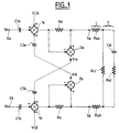
- La figure 1 représente le schéma synoptique d'un premier exemple de réalisation de l'étage différentiel selon l'invention.
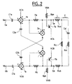
- La figure 2 représente le schéma synoptique d'un deuxième exemple de réalisation de l'étage différentiel selon l'invention.
- La figure 3 représente le schéma synoptique d'un troisième exemple de réalisation de l'étage différentiel selon l'invention.
- deux bornes d'entrée Ea et Eb recevant respectivement deux tensions variables Va et Vb, constituant un signal différentiel ;
- deux bornes de sorties Sa et Sb, fournissant une tension continue d'alimentation, et un signal alternatif, différentiels, à une ligne L reliée à un terminal distant T.
- un additionneur 1a à trois entrées, recevant respectivement :
- une tension continue VCA destinée à télé-alimenter le terminal distant T,
- la composante alternative de la tension d'entrée Va, via un condensateur C1a ;
- et une tension de contre-réaction via un condensateur C2a ;
- une résistance Ra en série entre la sortie de l'additionneur 1a et la borne de sortie Sa ;
- un soustracteur 2a ayant : une entrée non inversante reliée à la borne de sortie SA , une entrée inversante reliée à la sortie de l'additionneur 1a, et une sortie reliée au condensateur C2b pour lui fournir la tension de contre-réaction.
- un additionneur 1b à trois entrées, recevant respectivement :
- une tension continue VCB destinée à télé-alimenter le terminal distant T,
- la composante alternative de la tension d'entrée Vb, via un condensateur C1b ;
- et une tension de contre-réaction via un condensateur C2b ;
- une résistance Rb en série entre la sortie de l'additionneur 1b et la borne de sortie Sb ;
- un soustracteur 2b ayant : une entrée non inversante reliée à la borne de sortie Sb, une entrée inversante reliée à la sortie de l'additionneur 1b, et une sortie reliée au condensateur C2a pour lui fournir la tension de contre-réaction.
- un transistor Ta dont le collecteur est relié à la borne de sortie Sa, dont l'émetteur est relié directement à la tension continue d'alimentation VCA, et dont la base est reliée à une tension continue d'alimentation VBA, inférieure à VCA, par une résistance Rpa ;
- et un transistor Tb dont le collecteur est relié à la borne de sortie Sb, dont l'émetteur est relié directement à la tension continue d'alimentation VCB, et dont la base est reliée à la tension continue d'alimentation VBB, supérieure à VCB, par une résistance Rpb.
- un filtre passe-bas 3a en série avec un étage amplificateur 4a, qui relient la base du transistor Ta à la sortie du soustracteur 2a, la résistance Rpa étant supprimée ; ce filtre passe-bas 3a et cet étage amplificateur 4a étant alimentés par les mêmes moyens que l'additionneur 1a et le soustracteur 2a ;
- un filtre passe-bas 3b en série avec un étage amplificateur 4b, qui relient la base du transistor Tb à la sortie du soustracteur 2b, la résistance Rpb étant supprimée ; ce filtre passe-bas 3b et cet étage amplificateur 4b étant alimentés par les mêmes moyens que l'additionneur 1b et le soustracteur 2b.
Claims (3)
- Etage différentiel (1) de sortie d'équipement électronique, cet étage comportant deux voies reliant chacune une entrée (Ea ; Eb) à une sortie (Sa ; Sb) ; et comportant, sur chacune des voies, un premier moyen (1a) pour ajouter à la tension d'entrée de la voie considérée une tension de contre-réaction (Vrb ; Vra) de l'autre voie sur la voie considérée, et un deuxième moyen fournissant cette tension de contre-réaction de la voie considérée sur l'autre voie ;
caractérisé en ce que le second moyen pour fournir la tension de contre-réaction de l'autre voie sur la voie considérée comporte des moyens (C2a; C2b) pour fournir une tension de contre-réaction (Vrb ; Vra) fonction seulement de la composante alternative de la tension de sortie (Vsa ; Vsb) du premier moyen (1a ; 1b) de la voie considérée ;
et en ce qu'il comporte en outre, respectivement dans chaque voie, des moyens (1a ; 1b) pour additionner une tension continue (VCA ; VCB) à la tension de sortie de cette voie. - Etage différentiel selon la revendication 1, caractérisé en ce qu'il comporte en outre, respectivement dans chaque voie, des moyens (Ta ; Tb) pour additionner un courant continu supplémentaire au courant fourni par le premier moyen (1a ; 1b) de cette voie à la sortie de cette voie.
- Etage différentiel selon la revendication 2, caractérisé en ce qu'il comporte en outre, respectivement pour chaque voie, des moyens (3a, 4a ; 3b, 4b) pour asservir l'intensité du courant supplémentaire en fonction de la composante continue du courant fourni par le premier moyen (1a ; 1b) de cette voie à la sortie de cette voie, de façon à annuler la composante continue du courant fourni par le premier moyen (1a ; 1b).
Applications Claiming Priority (2)
| Application Number | Priority Date | Filing Date | Title |
|---|---|---|---|
| FR9904387A FR2792124B1 (fr) | 1999-04-08 | 1999-04-08 | Etage differentiel de sortie d'equipement electronique, qui permet de tele-alimenter un terminal |
| FR9904387 | 1999-04-08 |
Publications (2)
| Publication Number | Publication Date |
|---|---|
| EP1043832A1 true EP1043832A1 (fr) | 2000-10-11 |
| EP1043832B1 EP1043832B1 (fr) | 2008-01-23 |
Family
ID=9544159
Family Applications (1)
| Application Number | Title | Priority Date | Filing Date |
|---|---|---|---|
| EP00400641A Expired - Lifetime EP1043832B1 (fr) | 1999-04-08 | 2000-03-09 | Etage différentiel de sortie d'équipement électronique, qui permet de télé-alimenter un terminal |
Country Status (9)
| Country | Link |
|---|---|
| EP (1) | EP1043832B1 (fr) |
| KR (1) | KR20010014698A (fr) |
| AT (1) | ATE385067T1 (fr) |
| AU (1) | AU2521100A (fr) |
| CA (1) | CA2300631A1 (fr) |
| DE (1) | DE60037847T2 (fr) |
| FR (1) | FR2792124B1 (fr) |
| IL (1) | IL135320A0 (fr) |
| SG (1) | SG80093A1 (fr) |
Citations (3)
| Publication number | Priority date | Publication date | Assignee | Title |
|---|---|---|---|---|
| US4161693A (en) * | 1977-03-09 | 1979-07-17 | Airpax Electronics, Inc. | Clamped input common mode rejection amplifier |
| EP0449200A1 (fr) * | 1990-03-29 | 1991-10-02 | Alcatel Cit | Etage différentiel de sortie d'équipement électronique |
| US5345190A (en) * | 1993-08-02 | 1994-09-06 | Motorola, Inc. | Modular low voltage filter with common mode feedback |
-
1999
- 1999-04-08 FR FR9904387A patent/FR2792124B1/fr not_active Expired - Fee Related
-
2000
- 2000-03-09 EP EP00400641A patent/EP1043832B1/fr not_active Expired - Lifetime
- 2000-03-09 AT AT00400641T patent/ATE385067T1/de not_active IP Right Cessation
- 2000-03-09 DE DE60037847T patent/DE60037847T2/de not_active Expired - Lifetime
- 2000-03-13 CA CA002300631A patent/CA2300631A1/fr not_active Abandoned
- 2000-03-28 IL IL13532000A patent/IL135320A0/xx unknown
- 2000-03-31 AU AU25211/00A patent/AU2521100A/en not_active Abandoned
- 2000-03-31 SG SG200001873A patent/SG80093A1/en unknown
- 2000-04-07 KR KR1020000018139A patent/KR20010014698A/ko not_active Withdrawn
Patent Citations (3)
| Publication number | Priority date | Publication date | Assignee | Title |
|---|---|---|---|---|
| US4161693A (en) * | 1977-03-09 | 1979-07-17 | Airpax Electronics, Inc. | Clamped input common mode rejection amplifier |
| EP0449200A1 (fr) * | 1990-03-29 | 1991-10-02 | Alcatel Cit | Etage différentiel de sortie d'équipement électronique |
| US5345190A (en) * | 1993-08-02 | 1994-09-06 | Motorola, Inc. | Modular low voltage filter with common mode feedback |
Also Published As
| Publication number | Publication date |
|---|---|
| FR2792124B1 (fr) | 2001-06-15 |
| EP1043832B1 (fr) | 2008-01-23 |
| IL135320A0 (en) | 2001-05-20 |
| SG80093A1 (en) | 2001-04-17 |
| DE60037847T2 (de) | 2009-01-22 |
| FR2792124A1 (fr) | 2000-10-13 |
| KR20010014698A (ko) | 2001-02-26 |
| CA2300631A1 (fr) | 2000-10-08 |
| AU2521100A (en) | 2000-10-12 |
| ATE385067T1 (de) | 2008-02-15 |
| DE60037847D1 (de) | 2008-03-13 |
Similar Documents
| Publication | Publication Date | Title |
|---|---|---|
| EP0022561B1 (fr) | Dispositif d'alimentation d'un poste d'abonné | |
| FR2648285A1 (fr) | Systeme d'alimentation secourue a continuite du neutre | |
| EP0135412B1 (fr) | Circuit d'alimentation régulée notamment pour poste téléphonique | |
| EP0194177B1 (fr) | Circuit d'interface de ligne d'abonné téléphonique avec mode de veille à puissance réduite | |
| FR2500241A1 (fr) | Circuit d'alimentation par batterie pour une installation telephonique | |
| EP0119245A1 (fr) | Dispositif d'alimentation en courant d'un appareil telephonique d'abonne. | |
| FR2579393A1 (fr) | Circuit integrable monolithiquement pour la mesure de courants longitudinaux et transversaux dans une ligne de transmission bifilaire | |
| EP0078355B1 (fr) | Circuit d'interface comportant des moyens d'adaptation d'impédance | |
| EP1043832B1 (fr) | Etage différentiel de sortie d'équipement électronique, qui permet de télé-alimenter un terminal | |
| FR2526183A1 (fr) | Circuit regulateur | |
| FR2538648A1 (fr) | Circuit de suppression de signal de microphone pour poste telephonique | |
| FR2498851A1 (fr) | Circuit d'interface de ligne d'abonne | |
| EP0130261B1 (fr) | Circuit alimenteur en courant continu pour circuit d'interface de ligne | |
| US6728373B1 (en) | Differential output stage for electronic equipment providing a remote power feed to a terminal | |
| EP0457397B1 (fr) | circuit pour réguler le courant de ligne dans un poste téléphonique | |
| EP0864221B1 (fr) | Procede et appareil pour generer un signal d'appel | |
| FR2543761A1 (fr) | Filtre inductif de signaux electriques ayant une impedance reduite | |
| EP0103520B1 (fr) | Circuit d'entrée et d'alimentation pour filtre, notamment un filtre de récepteur de télécommande centralisée | |
| EP0189711A1 (fr) | Poste téléphonique d'abonné à haut parleur d'écoute amplifiée avec réduction de gain en cas d'alimentation insuffisante | |
| FR2581279A1 (fr) | Circuit telephonique, integrable monolithiquement, pour l'alimentation d'une ligne telephonique d'abonne | |
| US6167135A (en) | Method and apparatus for generating a ringing signal | |
| FR2640094A1 (fr) | Amplificateur du type cascode | |
| EP0838902A1 (fr) | Dispositif d'alignement d'un niveau de tension continue | |
| FR2474787A1 (fr) | Amplificateur a transfert de courant | |
| FR2601538A1 (fr) | Poste telephonique dont plusieurs fonctions electroniques sont alimentees par le courant de ligne et notamment la fonction d'ecoute amplifiee par haut-parleur |
Legal Events
| Date | Code | Title | Description |
|---|---|---|---|
| PUAI | Public reference made under article 153(3) epc to a published international application that has entered the european phase |
Free format text: ORIGINAL CODE: 0009012 |
|
| AK | Designated contracting states |
Kind code of ref document: A1 Designated state(s): AT BE CH CY DE DK ES FI FR GB GR IE IT LI LU MC NL PT SE |
|
| AX | Request for extension of the european patent |
Free format text: AL;LT;LV;MK;RO;SI |
|
| 17P | Request for examination filed |
Effective date: 20010411 |
|
| AKX | Designation fees paid |
Free format text: AT BE CH CY DE DK ES FI FR GB GR IE IT LI LU MC NL PT SE |
|
| RAP1 | Party data changed (applicant data changed or rights of an application transferred) |
Owner name: ALCATEL LUCENT |
|
| GRAP | Despatch of communication of intention to grant a patent |
Free format text: ORIGINAL CODE: EPIDOSNIGR1 |
|
| GRAS | Grant fee paid |
Free format text: ORIGINAL CODE: EPIDOSNIGR3 |
|
| GRAA | (expected) grant |
Free format text: ORIGINAL CODE: 0009210 |
|
| AK | Designated contracting states |
Kind code of ref document: B1 Designated state(s): AT BE CH CY DE DK ES FI FR GB GR IE IT LI LU MC NL PT SE |
|
| REG | Reference to a national code |
Ref country code: GB Ref legal event code: FG4D Free format text: NOT ENGLISH |
|
| REG | Reference to a national code |
Ref country code: CH Ref legal event code: EP |
|
| REG | Reference to a national code |
Ref country code: IE Ref legal event code: FG4D Free format text: LANGUAGE OF EP DOCUMENT: FRENCH |
|
| REF | Corresponds to: |
Ref document number: 60037847 Country of ref document: DE Date of ref document: 20080313 Kind code of ref document: P |
|
| GBT | Gb: translation of ep patent filed (gb section 77(6)(a)/1977) |
Effective date: 20080410 |
|
| NLV1 | Nl: lapsed or annulled due to failure to fulfill the requirements of art. 29p and 29m of the patents act | ||
| PG25 | Lapsed in a contracting state [announced via postgrant information from national office to epo] |
Ref country code: ES Free format text: LAPSE BECAUSE OF FAILURE TO SUBMIT A TRANSLATION OF THE DESCRIPTION OR TO PAY THE FEE WITHIN THE PRESCRIBED TIME-LIMIT Effective date: 20080504 Ref country code: FI Free format text: LAPSE BECAUSE OF FAILURE TO SUBMIT A TRANSLATION OF THE DESCRIPTION OR TO PAY THE FEE WITHIN THE PRESCRIBED TIME-LIMIT Effective date: 20080123 |
|
| PG25 | Lapsed in a contracting state [announced via postgrant information from national office to epo] |
Ref country code: AT Free format text: LAPSE BECAUSE OF FAILURE TO SUBMIT A TRANSLATION OF THE DESCRIPTION OR TO PAY THE FEE WITHIN THE PRESCRIBED TIME-LIMIT Effective date: 20080123 |
|
| BERE | Be: lapsed |
Owner name: ALCATEL LUCENT Effective date: 20080331 |
|
| PG25 | Lapsed in a contracting state [announced via postgrant information from national office to epo] |
Ref country code: PT Free format text: LAPSE BECAUSE OF FAILURE TO SUBMIT A TRANSLATION OF THE DESCRIPTION OR TO PAY THE FEE WITHIN THE PRESCRIBED TIME-LIMIT Effective date: 20080623 |
|
| REG | Reference to a national code |
Ref country code: IE Ref legal event code: FD4D |
|
| PG25 | Lapsed in a contracting state [announced via postgrant information from national office to epo] |
Ref country code: NL Free format text: LAPSE BECAUSE OF FAILURE TO SUBMIT A TRANSLATION OF THE DESCRIPTION OR TO PAY THE FEE WITHIN THE PRESCRIBED TIME-LIMIT Effective date: 20080123 Ref country code: DK Free format text: LAPSE BECAUSE OF FAILURE TO SUBMIT A TRANSLATION OF THE DESCRIPTION OR TO PAY THE FEE WITHIN THE PRESCRIBED TIME-LIMIT Effective date: 20080123 Ref country code: IE Free format text: LAPSE BECAUSE OF FAILURE TO SUBMIT A TRANSLATION OF THE DESCRIPTION OR TO PAY THE FEE WITHIN THE PRESCRIBED TIME-LIMIT Effective date: 20080123 Ref country code: SE Free format text: LAPSE BECAUSE OF FAILURE TO SUBMIT A TRANSLATION OF THE DESCRIPTION OR TO PAY THE FEE WITHIN THE PRESCRIBED TIME-LIMIT Effective date: 20080423 Ref country code: MC Free format text: LAPSE BECAUSE OF NON-PAYMENT OF DUE FEES Effective date: 20080331 |
|
| REG | Reference to a national code |
Ref country code: CH Ref legal event code: PL |
|
| PLBE | No opposition filed within time limit |
Free format text: ORIGINAL CODE: 0009261 |
|
| STAA | Information on the status of an ep patent application or granted ep patent |
Free format text: STATUS: NO OPPOSITION FILED WITHIN TIME LIMIT |
|
| 26N | No opposition filed |
Effective date: 20081024 |
|
| PG25 | Lapsed in a contracting state [announced via postgrant information from national office to epo] |
Ref country code: LI Free format text: LAPSE BECAUSE OF NON-PAYMENT OF DUE FEES Effective date: 20080331 Ref country code: CH Free format text: LAPSE BECAUSE OF NON-PAYMENT OF DUE FEES Effective date: 20080331 |
|
| PG25 | Lapsed in a contracting state [announced via postgrant information from national office to epo] |
Ref country code: BE Free format text: LAPSE BECAUSE OF NON-PAYMENT OF DUE FEES Effective date: 20080331 |
|
| PG25 | Lapsed in a contracting state [announced via postgrant information from national office to epo] |
Ref country code: CY Free format text: LAPSE BECAUSE OF FAILURE TO SUBMIT A TRANSLATION OF THE DESCRIPTION OR TO PAY THE FEE WITHIN THE PRESCRIBED TIME-LIMIT Effective date: 20080123 |
|
| PG25 | Lapsed in a contracting state [announced via postgrant information from national office to epo] |
Ref country code: IT Free format text: LAPSE BECAUSE OF FAILURE TO SUBMIT A TRANSLATION OF THE DESCRIPTION OR TO PAY THE FEE WITHIN THE PRESCRIBED TIME-LIMIT Effective date: 20080123 |
|
| PG25 | Lapsed in a contracting state [announced via postgrant information from national office to epo] |
Ref country code: LU Free format text: LAPSE BECAUSE OF NON-PAYMENT OF DUE FEES Effective date: 20080309 |
|
| PG25 | Lapsed in a contracting state [announced via postgrant information from national office to epo] |
Ref country code: GR Free format text: LAPSE BECAUSE OF FAILURE TO SUBMIT A TRANSLATION OF THE DESCRIPTION OR TO PAY THE FEE WITHIN THE PRESCRIBED TIME-LIMIT Effective date: 20080424 |
|
| REG | Reference to a national code |
Ref country code: GB Ref legal event code: 732E Free format text: REGISTERED BETWEEN 20130926 AND 20131002 |
|
| REG | Reference to a national code |
Ref country code: FR Ref legal event code: GC Effective date: 20131018 |
|
| REG | Reference to a national code |
Ref country code: FR Ref legal event code: RG Effective date: 20141016 |
|
| REG | Reference to a national code |
Ref country code: FR Ref legal event code: PLFP Year of fee payment: 16 |
|
| REG | Reference to a national code |
Ref country code: FR Ref legal event code: CA Effective date: 20150521 |
|
| REG | Reference to a national code |
Ref country code: FR Ref legal event code: CA Effective date: 20150521 |
|
| REG | Reference to a national code |
Ref country code: FR Ref legal event code: PLFP Year of fee payment: 17 |
|
| PGFP | Annual fee paid to national office [announced via postgrant information from national office to epo] |
Ref country code: FR Payment date: 20160321 Year of fee payment: 17 Ref country code: GB Payment date: 20160321 Year of fee payment: 17 |
|
| PGFP | Annual fee paid to national office [announced via postgrant information from national office to epo] |
Ref country code: DE Payment date: 20160330 Year of fee payment: 17 |
|
| REG | Reference to a national code |
Ref country code: DE Ref legal event code: R119 Ref document number: 60037847 Country of ref document: DE |
|
| GBPC | Gb: european patent ceased through non-payment of renewal fee |
Effective date: 20170309 |
|
| REG | Reference to a national code |
Ref country code: FR Ref legal event code: ST Effective date: 20171130 |
|
| PG25 | Lapsed in a contracting state [announced via postgrant information from national office to epo] |
Ref country code: DE Free format text: LAPSE BECAUSE OF NON-PAYMENT OF DUE FEES Effective date: 20171003 Ref country code: FR Free format text: LAPSE BECAUSE OF NON-PAYMENT OF DUE FEES Effective date: 20170331 |
|
| PG25 | Lapsed in a contracting state [announced via postgrant information from national office to epo] |
Ref country code: GB Free format text: LAPSE BECAUSE OF NON-PAYMENT OF DUE FEES Effective date: 20170309 |