EP1043772A2 - Method for packaging and mounting semiconductor device and device obtained thereby - Google Patents
Method for packaging and mounting semiconductor device and device obtained thereby Download PDFInfo
- Publication number
- EP1043772A2 EP1043772A2 EP00301898A EP00301898A EP1043772A2 EP 1043772 A2 EP1043772 A2 EP 1043772A2 EP 00301898 A EP00301898 A EP 00301898A EP 00301898 A EP00301898 A EP 00301898A EP 1043772 A2 EP1043772 A2 EP 1043772A2
- Authority
- EP
- European Patent Office
- Prior art keywords
- semiconductor
- semiconductor wafer
- resin
- thickness
- semiconductor device
- Prior art date
- Legal status (The legal status is an assumption and is not a legal conclusion. Google has not performed a legal analysis and makes no representation as to the accuracy of the status listed.)
- Granted
Links
Images




Classifications
-
- H—ELECTRICITY
- H10—SEMICONDUCTOR DEVICES; ELECTRIC SOLID-STATE DEVICES NOT OTHERWISE PROVIDED FOR
- H10W—GENERIC PACKAGES, INTERCONNECTIONS, CONNECTORS OR OTHER CONSTRUCTIONAL DETAILS OF DEVICES COVERED BY CLASS H10
- H10W76/00—Containers; Fillings or auxiliary members therefor; Seals
- H10W76/10—Containers or parts thereof
-
- H—ELECTRICITY
- H10—SEMICONDUCTOR DEVICES; ELECTRIC SOLID-STATE DEVICES NOT OTHERWISE PROVIDED FOR
- H10P—GENERIC PROCESSES OR APPARATUS FOR THE MANUFACTURE OR TREATMENT OF DEVICES COVERED BY CLASS H10
- H10P72/00—Handling or holding of wafers, substrates or devices during manufacture or treatment thereof
- H10P72/70—Handling or holding of wafers, substrates or devices during manufacture or treatment thereof for supporting or gripping
- H10P72/74—Handling or holding of wafers, substrates or devices during manufacture or treatment thereof for supporting or gripping using temporarily an auxiliary support
-
- H—ELECTRICITY
- H10—SEMICONDUCTOR DEVICES; ELECTRIC SOLID-STATE DEVICES NOT OTHERWISE PROVIDED FOR
- H10D—INORGANIC ELECTRIC SEMICONDUCTOR DEVICES
- H10D62/00—Semiconductor bodies, or regions thereof, of devices having potential barriers
- H10D62/10—Shapes, relative sizes or dispositions of the regions of the semiconductor bodies; Shapes of the semiconductor bodies
- H10D62/117—Shapes of semiconductor bodies
-
- H—ELECTRICITY
- H10—SEMICONDUCTOR DEVICES; ELECTRIC SOLID-STATE DEVICES NOT OTHERWISE PROVIDED FOR
- H10P—GENERIC PROCESSES OR APPARATUS FOR THE MANUFACTURE OR TREATMENT OF DEVICES COVERED BY CLASS H10
- H10P72/00—Handling or holding of wafers, substrates or devices during manufacture or treatment thereof
- H10P72/70—Handling or holding of wafers, substrates or devices during manufacture or treatment thereof for supporting or gripping
- H10P72/74—Handling or holding of wafers, substrates or devices during manufacture or treatment thereof for supporting or gripping using temporarily an auxiliary support
- H10P72/7402—Wafer tapes, e.g. grinding or dicing support tapes
-
- H—ELECTRICITY
- H10—SEMICONDUCTOR DEVICES; ELECTRIC SOLID-STATE DEVICES NOT OTHERWISE PROVIDED FOR
- H10W—GENERIC PACKAGES, INTERCONNECTIONS, CONNECTORS OR OTHER CONSTRUCTIONAL DETAILS OF DEVICES COVERED BY CLASS H10
- H10W74/00—Encapsulations, e.g. protective coatings
- H10W74/01—Manufacture or treatment
-
- H—ELECTRICITY
- H10—SEMICONDUCTOR DEVICES; ELECTRIC SOLID-STATE DEVICES NOT OTHERWISE PROVIDED FOR
- H10W—GENERIC PACKAGES, INTERCONNECTIONS, CONNECTORS OR OTHER CONSTRUCTIONAL DETAILS OF DEVICES COVERED BY CLASS H10
- H10W74/00—Encapsulations, e.g. protective coatings
- H10W74/10—Encapsulations, e.g. protective coatings characterised by their shape or disposition
- H10W74/111—Encapsulations, e.g. protective coatings characterised by their shape or disposition the semiconductor body being completely enclosed
- H10W74/129—Encapsulations, e.g. protective coatings characterised by their shape or disposition the semiconductor body being completely enclosed forming a chip-scale package [CSP]
-
- H—ELECTRICITY
- H10—SEMICONDUCTOR DEVICES; ELECTRIC SOLID-STATE DEVICES NOT OTHERWISE PROVIDED FOR
- H10P—GENERIC PROCESSES OR APPARATUS FOR THE MANUFACTURE OR TREATMENT OF DEVICES COVERED BY CLASS H10
- H10P72/00—Handling or holding of wafers, substrates or devices during manufacture or treatment thereof
- H10P72/70—Handling or holding of wafers, substrates or devices during manufacture or treatment thereof for supporting or gripping
- H10P72/74—Handling or holding of wafers, substrates or devices during manufacture or treatment thereof for supporting or gripping using temporarily an auxiliary support
- H10P72/7416—Handling or holding of wafers, substrates or devices during manufacture or treatment thereof for supporting or gripping using temporarily an auxiliary support used during dicing or grinding
-
- H—ELECTRICITY
- H10—SEMICONDUCTOR DEVICES; ELECTRIC SOLID-STATE DEVICES NOT OTHERWISE PROVIDED FOR
- H10P—GENERIC PROCESSES OR APPARATUS FOR THE MANUFACTURE OR TREATMENT OF DEVICES COVERED BY CLASS H10
- H10P72/00—Handling or holding of wafers, substrates or devices during manufacture or treatment thereof
- H10P72/70—Handling or holding of wafers, substrates or devices during manufacture or treatment thereof for supporting or gripping
- H10P72/74—Handling or holding of wafers, substrates or devices during manufacture or treatment thereof for supporting or gripping using temporarily an auxiliary support
- H10P72/7422—Handling or holding of wafers, substrates or devices during manufacture or treatment thereof for supporting or gripping using temporarily an auxiliary support used to protect an active side of a device or wafer
-
- H—ELECTRICITY
- H10—SEMICONDUCTOR DEVICES; ELECTRIC SOLID-STATE DEVICES NOT OTHERWISE PROVIDED FOR
- H10W—GENERIC PACKAGES, INTERCONNECTIONS, CONNECTORS OR OTHER CONSTRUCTIONAL DETAILS OF DEVICES COVERED BY CLASS H10
- H10W70/00—Package substrates; Interposers; Redistribution layers [RDL]
- H10W70/60—Insulating or insulated package substrates; Interposers; Redistribution layers
-
- H—ELECTRICITY
- H10—SEMICONDUCTOR DEVICES; ELECTRIC SOLID-STATE DEVICES NOT OTHERWISE PROVIDED FOR
- H10W—GENERIC PACKAGES, INTERCONNECTIONS, CONNECTORS OR OTHER CONSTRUCTIONAL DETAILS OF DEVICES COVERED BY CLASS H10
- H10W72/00—Interconnections or connectors in packages
- H10W72/01—Manufacture or treatment
- H10W72/013—Manufacture or treatment of die-attach connectors
- H10W72/01331—Manufacture or treatment of die-attach connectors using blanket deposition
-
- H—ELECTRICITY
- H10—SEMICONDUCTOR DEVICES; ELECTRIC SOLID-STATE DEVICES NOT OTHERWISE PROVIDED FOR
- H10W—GENERIC PACKAGES, INTERCONNECTIONS, CONNECTORS OR OTHER CONSTRUCTIONAL DETAILS OF DEVICES COVERED BY CLASS H10
- H10W72/00—Interconnections or connectors in packages
- H10W72/01—Manufacture or treatment
- H10W72/0198—Manufacture or treatment batch processes
-
- H—ELECTRICITY
- H10—SEMICONDUCTOR DEVICES; ELECTRIC SOLID-STATE DEVICES NOT OTHERWISE PROVIDED FOR
- H10W—GENERIC PACKAGES, INTERCONNECTIONS, CONNECTORS OR OTHER CONSTRUCTIONAL DETAILS OF DEVICES COVERED BY CLASS H10
- H10W72/00—Interconnections or connectors in packages
- H10W72/071—Connecting or disconnecting
- H10W72/072—Connecting or disconnecting of bump connectors
- H10W72/07251—Connecting or disconnecting of bump connectors characterised by changes in properties of the bump connectors during connecting
-
- H—ELECTRICITY
- H10—SEMICONDUCTOR DEVICES; ELECTRIC SOLID-STATE DEVICES NOT OTHERWISE PROVIDED FOR
- H10W—GENERIC PACKAGES, INTERCONNECTIONS, CONNECTORS OR OTHER CONSTRUCTIONAL DETAILS OF DEVICES COVERED BY CLASS H10
- H10W72/00—Interconnections or connectors in packages
- H10W72/20—Bump connectors, e.g. solder bumps or copper pillars; Dummy bumps; Thermal bumps
-
- H—ELECTRICITY
- H10—SEMICONDUCTOR DEVICES; ELECTRIC SOLID-STATE DEVICES NOT OTHERWISE PROVIDED FOR
- H10W—GENERIC PACKAGES, INTERCONNECTIONS, CONNECTORS OR OTHER CONSTRUCTIONAL DETAILS OF DEVICES COVERED BY CLASS H10
- H10W72/00—Interconnections or connectors in packages
- H10W72/20—Bump connectors, e.g. solder bumps or copper pillars; Dummy bumps; Thermal bumps
- H10W72/251—Materials
- H10W72/252—Materials comprising solid metals or solid metalloids, e.g. PbSn, Ag or Cu
-
- H—ELECTRICITY
- H10—SEMICONDUCTOR DEVICES; ELECTRIC SOLID-STATE DEVICES NOT OTHERWISE PROVIDED FOR
- H10W—GENERIC PACKAGES, INTERCONNECTIONS, CONNECTORS OR OTHER CONSTRUCTIONAL DETAILS OF DEVICES COVERED BY CLASS H10
- H10W72/00—Interconnections or connectors in packages
- H10W72/90—Bond pads, in general
- H10W72/921—Structures or relative sizes of bond pads
- H10W72/922—Bond pads being integral with underlying chip-level interconnections
- H10W72/9223—Bond pads being integral with underlying chip-level interconnections with redistribution layers [RDL]
-
- H—ELECTRICITY
- H10—SEMICONDUCTOR DEVICES; ELECTRIC SOLID-STATE DEVICES NOT OTHERWISE PROVIDED FOR
- H10W—GENERIC PACKAGES, INTERCONNECTIONS, CONNECTORS OR OTHER CONSTRUCTIONAL DETAILS OF DEVICES COVERED BY CLASS H10
- H10W72/00—Interconnections or connectors in packages
- H10W72/90—Bond pads, in general
- H10W72/921—Structures or relative sizes of bond pads
- H10W72/923—Bond pads having multiple stacked layers
-
- H—ELECTRICITY
- H10—SEMICONDUCTOR DEVICES; ELECTRIC SOLID-STATE DEVICES NOT OTHERWISE PROVIDED FOR
- H10W—GENERIC PACKAGES, INTERCONNECTIONS, CONNECTORS OR OTHER CONSTRUCTIONAL DETAILS OF DEVICES COVERED BY CLASS H10
- H10W72/00—Interconnections or connectors in packages
- H10W72/90—Bond pads, in general
- H10W72/941—Dispositions of bond pads
- H10W72/9415—Dispositions of bond pads relative to the surface, e.g. recessed, protruding
-
- H—ELECTRICITY
- H10—SEMICONDUCTOR DEVICES; ELECTRIC SOLID-STATE DEVICES NOT OTHERWISE PROVIDED FOR
- H10W—GENERIC PACKAGES, INTERCONNECTIONS, CONNECTORS OR OTHER CONSTRUCTIONAL DETAILS OF DEVICES COVERED BY CLASS H10
- H10W72/00—Interconnections or connectors in packages
- H10W72/90—Bond pads, in general
- H10W72/941—Dispositions of bond pads
- H10W72/942—Dispositions of bond pads relative to underlying supporting features, e.g. bond pads, RDLs or vias
Definitions
- the present invention relates to a semiconductor device and a manufacturing method for the same and, more particularly, to a package of the semiconductor device.
- a semiconductor device shown in Fig. 9 has electrode pads 2 formed on a semiconductor element 1 having a thickness of 400 ⁇ m, and posts 3 composed of copper or the like electrically connected to the electrode pads 2 are formed thereon.
- the surface of the semiconductor element and the posts 3 are sealed by a resin 4 that is approximately 100 ⁇ m thick.
- Bumps 5 composed of solder or the like are formed on the posts 3 exposed on a resin surface.
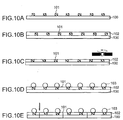
- Posts 101 made of copper or the like are formed on a wafer 100, which is a semiconductor substrate as illustrated in Fig. 10-A.
- a resin 102 is charged to cover the entire water as illustrated in Fig. 10-B.
- the entire surface is polished until the posts 101 are exposed on the surface as illustrated in Fig. 10-C.
- bump electrodes 103 made of solder or the like are formed on the surfaces of the posts 101 as illustrated in Fig. 10-D.
- the wafer is cut and divided into individual semiconductor devices as illustrated in Fig. 10-E.
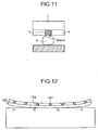
- the conventional structure and manufacturing method have been posing problems including one in which a crack occurs at a junction between a semiconductor element and a mounting substrate due to thermal stress when mounting a semiconductor device on a printed board or the like (refer to Fig. 11).
- a crack occurs at a junction between a semiconductor element and a mounting substrate due to thermal stress when mounting a semiconductor device on a printed board or the like.
- a wafer develops a warp when resin sealing is performed.
- a warped wafer is difficult to be fixed when dividing it into individual segments as shown in Fig. 12.
- a semiconductor device in accordance with the present invention has a semiconductor element having a thickness of 200 ⁇ m or less, an electrode pad formed on the semiconductor element, a post electrically connected to the electrode pad, and a sealing resin for sealing a surface of the semiconductor element whereon circuitry is formed and the post.
- a manufacturing method for a semiconductor device in accordance with the present invention includes a step for forming an electrode pad on a main surface of a semiconductor wafer, a step for forming a post to be electrically connected to the electrode pad, a step for resin-sealing the main surface of the semiconductor wafer and the post, a step for forming a groove from a resin surface to a predetermined depth of the semiconductor wafer, and a step for polishing a rear surface of the semiconductor wafer to a bottom of the groove and dividing the semiconductor wafer into individual semiconductor devices.
- a mounting method for a semiconductor device in accordance with the present invention includes a step for preparing a semiconductor device in which a main surface of a semiconductor element having a thickness of 200 ⁇ m or less has been resin-sealed, a step for disposing the semiconductor device on a mounting substrate, and a step for connecting the semiconductor device and the mounting substrate by heat treatment.
- Fig. 1 is a diagram showing a structure of a semiconductor device in a first embodiment according to the present invention.
- the first embodiment of the invention will be described.
- the same components as those in Fig. 8 will be assigned the same reference numerals, and descriptions will be given thereof.
- a thickness of a semiconductor element or a resin will be indicated by dashed lines or the like.
- a semiconductor element 1 is formed to be thinner than 400 ⁇ m, which is a thickness in a conventional structure. In this embodiment, the semiconductor element 1 is 100 ⁇ m thick.
- Aluminum electrode pads 2 are formed at predetermined locations on a main surface of the semiconductor element 1.
- Posts 3 composed of copper are formed on the semiconductor element, the height of the posts 3 being 50 ⁇ m.
- the posts 3 are electrically connected to the aluminum electrode pads 2.
- the main surface (a surface where a circuit is formed) of the semiconductor element 1 and the posts 3 are sealed by a resin 4, the thickness of the resin 4 being 50 ⁇ m, which is identical to the thickness of the posts 3.
- Bump electrodes 5 are formed on the resin 4.
- the bump electrodes 5 composed of solder or the like are formed on the posts 3 exposed on the surface of the resin 4.
- Fig. 2-A is a diagram showing results of a temperature cycle test conducted with a semiconductor device mounted on a mounting substrate such as a printed circuit board.
- the axis of abscissa indicates the thickness of a semiconductor element, while the axis of ordinates indicates the number of cycles at which a crack occurs in a junction (a solder ball in this embodiment) between the semiconductor device and the mounting substrate in relation to a distortion observed between the mounting substrate and the semiconductor device.
- Fig. 2-A shows that the maximum distortion of a junction decreases as the thickness of the semiconductor element is decreased.
- the effect is remarkably noticeable when the thickness of the semiconductor element is reduced to 200 ⁇ m or less.
- Fig. 2-B shows temperature characteristics observed when the thickness of the resin sealing the main surface of the semiconductor element is changed, with the thickness of the semiconductor element being left unchanged. Data shown in Fig. 2-B has been obtained when the thickness of the semiconductor element was set to 200 ⁇ m, and the thickness of the resin was changed to about 50 ⁇ m, about 60 ⁇ m, about 100 ⁇ m, and about 150 ⁇ m, respectively.
- the maximum distortion is reduced when the ratio of the thickness of the semiconductor element to the thickness of the resin is set to 2 to 1, or 1 to 1 as in the case of the present invention.
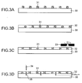
- Fig. 3 and Fig. 4 illustrate a manufacturing method for a semiconductor device of the first embodiment in accordance with the invention.
- Copper posts 31 having a height of approximately 50 ⁇ m are formed on a main surface (where a circuit is formed) of a semiconductor wafer 30 by electroplating or the like as shown in Fig. 3-A.
- the posts 31 are electrically connected to electrode pads (not shown) formed on the wafer 30.
- a resin 32 is charged according to a transfer molding method, a potting method, a printing method, etc. to cover the main surface of the semiconductor wafer 30 and the posts 31 (see Fig. 3-B).
- the semiconductor wafer 30 at this stage has a sufficient thickness to prevent a warp from taking place due to stress of the resin 32, etc.
- the surface of the resin 32 is polished by a polishing blade 33 until the posts 31 buried in the resin 32 are exposed and the heights of the resin 32 and the posts 31 reach 50 ⁇ m (see Fig. 3-C).
- Grooves 35 are formed in the surface covered with the resin 32 by an outer peripheral blade 34 that rotates at a high speed, the grooves 35 being formed at locations where the wafer is divided into individual semiconductor devices later.
- the depth of the grooves 35 is determined on the basis of a thickness of the semiconductor elements in the final individual semiconductor devices.
- the thickness of the semiconductor element 1 is set to 100 ⁇ m, so that the grooves having a depth of 120 ⁇ m are formed in the semiconductor wafer 30.
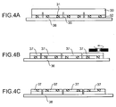
- a grinding tape 36 is attached to the surface of the substrate whereon the resin has been deposited.
- the grinding tape can be easily peeled off by radiating ultraviolet rays thereby to weaken its adhesive strength.
- the surface to which the grinding tape 36 has been attached is fixed onto a grinding stage (not shown) as shown in Fig. 4-A. Then, the entire rear surface of the wafer 30 is polished with the wafer 30 secured to the grinding stage until the bottoms of the grooves 35, which have been formed in the preceding step, are reached.
- polishing the rear surface of the wafer 30 until the bottoms are reached causes the wafer 30 to be divided into individual semiconductor devices.
- the separated semiconductor devices 37 from the wafer are arranged on the grinding tape 36 as shown in Fig. 4-B.
- a mounting tape 38 is attached to the rear surface, which has been polished, before the semiconductor devices 37 are moved to the following step wherein bump electrodes or the like are formed as necessary.
- the wafer is first sealed with the sufficiently thick resin, so that there should be no danger of a warp occurring in wafer at this stage. Thereafter, the grooves are formed in the wafer from the resin side, then the entire rear surface of the wafer is polished to the bottoms of the grooves thereby to divide the wafer into separate semiconductor devices.
- the method described above makes it possible to solve the warp problem with a wafer when fixing the wafer.
- the manufacturing method in accordance with the present invention also makes it possible to provide a semiconductor device having a thinner semiconductor element than a conventional semiconductor element.
- Fig. 5 shows a structure of a semiconductor device in a second embodiment in accordance with the present invention.
- a semiconductor element 1 is formed to be thinner than a conventional structure that measures 400 ⁇ m.
- a central portion 11 of the semiconductor element 1 in this embodiment is 100 ⁇ m thick.
- the thickness of the semiconductor device 1 is smaller in a peripheral portion 12 thereof than in the central portion 11 thereof, meaning that the peripheral portion of the semiconductor element 1 has a stepped portion 6.
- the stepped portion 6 is formed on a main surface side (the surface where circuitry is formed) of the semiconductor element.
- a depth of the stepped portion 6, i.e. a distance from the surface of the central portion to the top of the peripheral portion 12, is approximately 30 ⁇ m.
- Aluminum electrode pads 2 are formed at predetermined locations on the main surface portion of the semiconductor element 1, and copper posts 3 are also formed on the semiconductor element 1, the height of the posts 3 being 50 ⁇ m.
- the posts 3 are electrically connected to the aluminum electrode pads 2.
- the main surface of the semiconductor element 1 and the posts 3 are sealed by a resin 4 which has a thickness of 50 ⁇ m, which is identical to the height of the posts 3.
- Bump electrodes 5 are formed on the resin 4.
- the bump electrodes 5 composed of solder or the like are formed on the posts 3 exposed on the surface of the resin 4.
- the peripheral portion 12 of the semiconductor element 1 is thinner than the central portion 11, forming the stepped portion 6.
- the stepped portion 6 is formed on each of four sides to surround the central portion 11 of the semiconductor element. This arrangement prevents cracks or the like during mounting as in the case of the first embodiment.
- the presence of the stepped portion adds to a portion of contact between the resin 4 and the semiconductor element 1 at the peripheral portion 12 of the semiconductor element 1, thus minimizing the chances of peeling off of the resin. Moreover, even if water enters through an interface between the semiconductor element 1 and the resin, the water will not reach the central portion where circuitry is formed.
- Fig. 6 and Fig. 7 illustrate a manufacturing method for a semiconductor device according to the second embodiment of the invention.
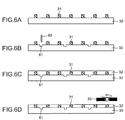
- Copper posts 31 having a height of approximately 50 ⁇ m are formed on the main surface of a semiconductor wafer 30 by electroplating or the like (see Fig. 6-A).
- the posts 31 are electrically connected to electrode pads (not shown) formed on the wafer 30.
- First grooves 61 are formed in the main surface of the semiconductor wafer 30 by an outer peripheral blade 60 that are rotated at a high speed.
- the first grooves 61 are formed in portions that provide the peripheral portions of individual semiconductor elements.
- the thickness of the blade 60 used for forming the first grooves is approximately 50 ⁇ m.
- the grooves 61 are formed to have a width that is 1 to 5 ⁇ m larger than the blade thickness.
- the depth of the first grooves 61 is 30 ⁇ m (see Fig. 6-B).
- the main surface, where circuitry is formed, of the semiconductor wafer 30 is filled with a resin 32 by a transfer molding method, a potting method, a printing method, etc. (see Fig. 6-C).
- the semiconductor wafer 30 in this step is sufficiently thick, so that it does not develop a warp caused primarily by stress of the resin 32.
- the surface of the resin 32 is polished by a polishing blade 33 until the posts 31, which have been buried in the resin, are exposed, and the heights of the resin 32 and the posts 31 reach 50 ⁇ m (see Fig. 6-D).
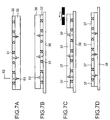
- Second grooves 63 are formed using an outer peripheral blade 62, which rotates at a high speed, in the surface covered with the resin 32 as illustrated in Fig. 7-A.
- the second grooves 63 having a width smaller than that of the first grooves 61 are formed in the first grooves 61, an enlarged view thereof being given in Fig. 8.
- the thickness of the blade 62 for forming the second grooves 63 is approximately 30 ⁇ m.
- the depth of the second grooves 63 is determined on the basis of a thickness of the semiconductor elements in the final individual semiconductor devices.
- the thickness of central portions of the semiconductor elements is set to 100 ⁇ m, so that the grooves having a depth of 120 ⁇ m measured from the main surface of the semiconductor wafer 30 are formed in the semiconductor wafer 30.
- a grinding tape 36 is attached to the surface whereon the resin has been deposited.
- the grinding tape 36 can be easily peeled off by radiating ultraviolet rays thereby to weaken its adhesive strength.
- the grinding tape 36 is fixed onto a grinding stage (not shown) as shown in Fig. 7-B. Then, the rear surface of the wafer 30 is polished with the wafer 30 secured to the grinding stage until the bottoms of the second grooves 63, which have been formed in the preceding step, are reached (see Fig. 7-C).
- Polishing the rear surface of the wafer until the bottoms of the second grooves 63 are reached causes the wafer 30 to be divided into individual semiconductor devices.
- separated semiconductor devices 37 are arranged on the grinding tape 36.
- a mounting tape 38 is attached to the polished rear surface of the wafer before the semiconductor devices 37 are supplied to the following step.
- the depth of the first grooves is set to 30 ⁇ m. Forming the first grooves 61 to be excessively deep would add to influences of resin stress. Experiments performed by the inventors have revealed that, if the depth of the first grooves is set to exceed 30 ⁇ m, then a wafer incurs influences exerted by the resin stress, resulting in a likelihood of a warp when the wafer is fixed.
- the first grooves 61 are formed so that they are deeper than the portion of the wafer surface where circuitry is formed, namely, in a range of about 10 ⁇ m to about 30 ⁇ m.
- the method described above makes it possible to solve the warp problem with a wafer when fixing the wafer.
- a wafer is unlikely to incur a warp or the like when it is fixed, as in the case of the manufacturing method for a semiconductor device according to the first embodiment.
- first grooves makes it possible to provide a semiconductor device that minimizes chances for a resin to peel off and that is capable of preventing the entry of water.
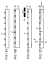
- Fig. 13 and Fig. 14 illustrate another manufacturing method for a semiconductor device in accordance with the present invention.
- the following will describe the manufacturing method according to the invention, taking the first embodiment as an example.
- like components as those in Fig. 3 and Fig. 4 will be assigned like reference numerals.
- the process up to the step wherein the resin 32 on the semiconductor wafer 30 is polished by the polishing blade 33 is the same as that of the first embodiment (Fig. 13-A through Fig. 13-C).
- grooves 35 are formed using an outer peripheral blade 34, which rotates at a high speed, in a surface covered with a resin 32.
- the grooves 35 are formed at locations where the wafer is divided into individual semiconductor devices.
- the third embodiment differs from the first embodiment in the depth of the grooves.
- the thickness of a semiconductor element 1 is set to 100 ⁇ m, so that the grooves having a depth of 50 ⁇ m are formed in the semiconductor wafer 30.
- a grinding tape 36 is attached to the surface of a substrate whereon the resin has been deposited.
- the grinding tape can be easily peeled off by radiating ultraviolet rays thereby to weaken its adhesive strength.
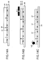
- the surface to which the grinding tape 36 has been attached is fixed onto a grinding stage (not shown) as shown in Fig. 14-A.
- the entire rear surface of the wafer 30 is polished with the wafer 30 secured to the grinding stage until a level which is 50 ⁇ m above the bottoms of the grooves 35 is reached.
- the polishing is finished when the thickness of the semiconductor wafer 30 reaches 100 ⁇ m.
- portions where the grooves 35 have been formed develop cracks that reach the rear surface of the semiconductor wafer 30 primarily due to stress during the polishing (see Fig. 14-B).
- the semiconductor devices are divided into individual pieces.
- the same manufacturing method as that of the third embodiment can be implemented in the manufacturing method according to the second embodiment by setting the depth of the second grooves to 100 ⁇ m.
- grooves formed from the main surface side of a semiconductor wafer can be made shorter, thus permitting reduced stress applied to individual semiconductor devices.
- the semiconductor devices of the first and second embodiments in accordance with the present invention are disposed on a mounting substrate such as a printed circuit board, and after that, they are connected onto a mounting substrate by heat treatment such as reflow of solder.
- a mounting substrate such as a printed circuit board
- heat treatment such as reflow of solder.
- a semiconductor device in accordance with the present invention makes it possible to reduce cracks in a junction between a mounting substrate and a semiconductor device.
- a manufacturing method in accordance with the present invention makes it possible to solve problems such as a warp of a wafer when the wafer is fixed.
Landscapes
- Dicing (AREA)
- Structures Or Materials For Encapsulating Or Coating Semiconductor Devices Or Solid State Devices (AREA)
- Encapsulation Of And Coatings For Semiconductor Or Solid State Devices (AREA)
- Mechanical Treatment Of Semiconductor (AREA)
Abstract
Description
- The present invention relates to a semiconductor device and a manufacturing method for the same and, more particularly, to a package of the semiconductor device.
- In recent years, with the increasing mounting density of semiconductor devices, chip-size packages or similar types of semiconductor devices are drawing attention.
- Hitherto, as such a type of chip-size packages, one shown in Fig. 9 has been available. A semiconductor device shown in Fig. 9 has
electrode pads 2 formed on asemiconductor element 1 having a thickness of 400 µm, andposts 3 composed of copper or the like electrically connected to theelectrode pads 2 are formed thereon. The surface of the semiconductor element and theposts 3 are sealed by aresin 4 that is approximately 100 µm thick.Bumps 5 composed of solder or the like are formed on theposts 3 exposed on a resin surface. - Referring to Fig. 10, a manufacturing method for a conventional semiconductor device will be described.
-
Posts 101 made of copper or the like are formed on awafer 100, which is a semiconductor substrate as illustrated in Fig. 10-A. In this state, aresin 102 is charged to cover the entire water as illustrated in Fig. 10-B. The entire surface is polished until theposts 101 are exposed on the surface as illustrated in Fig. 10-C. Then,bump electrodes 103 made of solder or the like are formed on the surfaces of theposts 101 as illustrated in Fig. 10-D. Lastly, the wafer is cut and divided into individual semiconductor devices as illustrated in Fig. 10-E. - The conventional structure and manufacturing method have been posing problems including one in which a crack occurs at a junction between a semiconductor element and a mounting substrate due to thermal stress when mounting a semiconductor device on a printed board or the like (refer to Fig. 11). In the manufacturing method for the conventional semiconductor devices, if the stress of a sealing resin is high, then a wafer develops a warp when resin sealing is performed. A warped wafer is difficult to be fixed when dividing it into individual segments as shown in Fig. 12.
- To solve the problems mentioned above, a semiconductor device in accordance with the present invention has a semiconductor element having a thickness of 200 µm or less, an electrode pad formed on the semiconductor element, a post electrically connected to the electrode pad, and a sealing resin for sealing a surface of the semiconductor element whereon circuitry is formed and the post.
- Furthermore, a manufacturing method for a semiconductor device in accordance with the present invention includes a step for forming an electrode pad on a main surface of a semiconductor wafer, a step for forming a post to be electrically connected to the electrode pad, a step for resin-sealing the main surface of the semiconductor wafer and the post, a step for forming a groove from a resin surface to a predetermined depth of the semiconductor wafer, and a step for polishing a rear surface of the semiconductor wafer to a bottom of the groove and dividing the semiconductor wafer into individual semiconductor devices.
- A mounting method for a semiconductor device in accordance with the present invention includes a step for preparing a semiconductor device in which a main surface of a semiconductor element having a thickness of 200 µm or less has been resin-sealed, a step for disposing the semiconductor device on a mounting substrate, and a step for connecting the semiconductor device and the mounting substrate by heat treatment.
-
- Fig. 1 is a diagram showing a structure of a semiconductor device of a first embodiment in accordance with the present invention.
- Fig. 2 is a diagram showing a temperature cycle characteristic of a semiconductor device in accordance with the present invention.
- Fig. 3 and Fig. 4 are process diagrams showing steps of a manufacturing method for the semiconductor device of the first embodiment in accordance with the present invention.
- Fig. 5 is a diagram showing a structure of a semiconductor device of a second embodiment in accordance with the present invention.
- Fig. 6 and Fig. 7 are process diagrams showing steps of a manufacturing method for the semiconductor device of the second embodiment in accordance with the present invention.
- Fig. 8 is an enlarged view of a groove in the manufacturing method for the semiconductor device of the second embodiment in accordance with the present invention.
- Fig. 9 is a diagram showing a structure of a conventional semiconductor element.
- Fig. 10 is a process diagram showing steps of a manufacturing method for a conventional semiconductor element.
- Fig. 11 and Fig. 12 are diagrams showing problems with a conventional art.
- Fig. 13 and Fig. 14 are process diagrams showing steps of a manufacturing method for a semiconductor device of a third embodiment in accordance with the present invention.
-
- Fig. 1 is a diagram showing a structure of a semiconductor device in a first embodiment according to the present invention. In conjunction with Fig. 1, the first embodiment of the invention will be described. The same components as those in Fig. 8 will be assigned the same reference numerals, and descriptions will be given thereof. In the drawings, a thickness of a semiconductor element or a resin will be indicated by dashed lines or the like.
- A
semiconductor element 1 is formed to be thinner than 400 µm, which is a thickness in a conventional structure. In this embodiment, thesemiconductor element 1 is 100 µm thick. -
Aluminum electrode pads 2 are formed at predetermined locations on a main surface of thesemiconductor element 1.Posts 3 composed of copper are formed on the semiconductor element, the height of theposts 3 being 50 µm. Theposts 3 are electrically connected to thealuminum electrode pads 2. - The main surface (a surface where a circuit is formed) of the
semiconductor element 1 and theposts 3 are sealed by aresin 4, the thickness of theresin 4 being 50 µm, which is identical to the thickness of theposts 3.Bump electrodes 5 are formed on theresin 4. In this embodiment, thebump electrodes 5 composed of solder or the like are formed on theposts 3 exposed on the surface of theresin 4. - Fig. 2-A is a diagram showing results of a temperature cycle test conducted with a semiconductor device mounted on a mounting substrate such as a printed circuit board. In Fig. 2-A, the axis of abscissa indicates the thickness of a semiconductor element, while the axis of ordinates indicates the number of cycles at which a crack occurs in a junction (a solder ball in this embodiment) between the semiconductor device and the mounting substrate in relation to a distortion observed between the mounting substrate and the semiconductor device.
- Due to a difference in thermal expansion coefficient, a distortion takes place between the semiconductor device and the mounting substrate. Decreasing the thickness of the
semiconductor element 1 adds to the flexibility of the semiconductor element itself; hence, the semiconductor element itself will absorb the distortion during heating. Fig. 2-A shows that the maximum distortion of a junction decreases as the thickness of the semiconductor element is decreased. - Furthermore, as the semiconductor element is made thinner, the number of temperature cycles at which a crack appears in the solder ball increases.
- The effect is remarkably noticeable when the thickness of the semiconductor element is reduced to 200 µm or less.
- Fig. 2-B shows temperature characteristics observed when the thickness of the resin sealing the main surface of the semiconductor element is changed, with the thickness of the semiconductor element being left unchanged. Data shown in Fig. 2-B has been obtained when the thickness of the semiconductor element was set to 200 µm, and the thickness of the resin was changed to about 50 µm, about 60 µm, about 100 µm, and about 150 µm, respectively.
- As compared with a case wherein the ratio of the thickness of the semiconductor element to the thickness of the resin is set to 4 to 1, the maximum distortion is reduced when the ratio of the thickness of the semiconductor element to the thickness of the resin is set to 2 to 1, or 1 to 1 as in the case of the present invention. This indicates that the flexibility of the semiconductor element itself increases with resultant better temperature characteristics when the thickness of the resin is greater than the thickness of the semiconductor element. Marked effect can be observed when the thickness of the resin is set to a half or more of the thickness of the semiconductor element.
- More detailed experiments and simulations carried out by the inventors have revealed that, in the semiconductor device in accordance with the present invention, cracks that occur primarily when mounting the semiconductor device on a substrate can be sufficiently restrained by setting the thickness of the semiconductor element to 200 µm or less and by setting the thickness of the resin to a half or more of the thickness of the semiconductor element.
- Fig. 3 and Fig. 4 illustrate a manufacturing method for a semiconductor device of the first embodiment in accordance with the invention.
- Referring to Fig. 3 and Fig. 4, the manufacturing method for a semiconductor device of the first embodiment in accordance with the invention will be described.
-
Copper posts 31 having a height of approximately 50 µm are formed on a main surface (where a circuit is formed) of a semiconductor wafer 30 by electroplating or the like as shown in Fig. 3-A. Theposts 31 are electrically connected to electrode pads (not shown) formed on thewafer 30. - A
resin 32 is charged according to a transfer molding method, a potting method, a printing method, etc. to cover the main surface of thesemiconductor wafer 30 and the posts 31 (see Fig. 3-B). - The semiconductor wafer 30 at this stage has a sufficient thickness to prevent a warp from taking place due to stress of the
resin 32, etc. - The surface of the
resin 32 is polished by apolishing blade 33 until theposts 31 buried in theresin 32 are exposed and the heights of theresin 32 and theposts 31 reach 50 µm (see Fig. 3-C). -
Grooves 35 are formed in the surface covered with theresin 32 by an outerperipheral blade 34 that rotates at a high speed, thegrooves 35 being formed at locations where the wafer is divided into individual semiconductor devices later. The depth of thegrooves 35 is determined on the basis of a thickness of the semiconductor elements in the final individual semiconductor devices. In this embodiment, the thickness of thesemiconductor element 1 is set to 100 µm, so that the grooves having a depth of 120 µm are formed in thesemiconductor wafer 30. The depth from the resin surface to the bottoms of thegrooves 35 formed in this process step will be a sum of the resin thickness and the depth of the grooves in the wafer, namely, 50 + 120 = 170 µm (see Fig. 3-D). - Then, a grinding
tape 36 is attached to the surface of the substrate whereon the resin has been deposited. The grinding tape can be easily peeled off by radiating ultraviolet rays thereby to weaken its adhesive strength. - The surface to which the grinding
tape 36 has been attached is fixed onto a grinding stage (not shown) as shown in Fig. 4-A. Then, the entire rear surface of thewafer 30 is polished with thewafer 30 secured to the grinding stage until the bottoms of thegrooves 35, which have been formed in the preceding step, are reached. - Polishing the rear surface of the
wafer 30 until the bottoms are reached causes thewafer 30 to be divided into individual semiconductor devices. Thus, the separatedsemiconductor devices 37 from the wafer are arranged on the grindingtape 36 as shown in Fig. 4-B. - A mounting
tape 38 is attached to the rear surface, which has been polished, before thesemiconductor devices 37 are moved to the following step wherein bump electrodes or the like are formed as necessary. - In the manufacturing method in this embodiment, the wafer is first sealed with the sufficiently thick resin, so that there should be no danger of a warp occurring in wafer at this stage. Thereafter, the grooves are formed in the wafer from the resin side, then the entire rear surface of the wafer is polished to the bottoms of the grooves thereby to divide the wafer into separate semiconductor devices.
- The method described above makes it possible to solve the warp problem with a wafer when fixing the wafer.
- Even when the semiconductor element finally becomes thin, the individual semiconductor devices are sufficiently smaller than the wafer, thus solving the stress problem attributable to a resin. The manufacturing method in accordance with the present invention also makes it possible to provide a semiconductor device having a thinner semiconductor element than a conventional semiconductor element.
- Fig. 5 shows a structure of a semiconductor device in a second embodiment in accordance with the present invention.
- Referring to Fig. 5, the second embodiment will now be described. In the description, like components as those in Fig. 1 will be assigned like reference numerals.
- A
semiconductor element 1 is formed to be thinner than a conventional structure that measures 400 µm. Acentral portion 11 of thesemiconductor element 1 in this embodiment is 100 µm thick. The thickness of thesemiconductor device 1 is smaller in aperipheral portion 12 thereof than in thecentral portion 11 thereof, meaning that the peripheral portion of thesemiconductor element 1 has a steppedportion 6. The steppedportion 6 is formed on a main surface side (the surface where circuitry is formed) of the semiconductor element. A depth of the steppedportion 6, i.e. a distance from the surface of the central portion to the top of theperipheral portion 12, is approximately 30 µm. -
Aluminum electrode pads 2 are formed at predetermined locations on the main surface portion of thesemiconductor element 1, andcopper posts 3 are also formed on thesemiconductor element 1, the height of theposts 3 being 50 µm. Theposts 3 are electrically connected to thealuminum electrode pads 2. - The main surface of the
semiconductor element 1 and theposts 3 are sealed by aresin 4 which has a thickness of 50 µm, which is identical to the height of theposts 3.Bump electrodes 5 are formed on theresin 4. In this embodiment, thebump electrodes 5 composed of solder or the like are formed on theposts 3 exposed on the surface of theresin 4. - In the semiconductor device according to the present invention, the
peripheral portion 12 of thesemiconductor element 1 is thinner than thecentral portion 11, forming the steppedportion 6. The steppedportion 6 is formed on each of four sides to surround thecentral portion 11 of the semiconductor element. This arrangement prevents cracks or the like during mounting as in the case of the first embodiment. - The presence of the stepped portion adds to a portion of contact between the
resin 4 and thesemiconductor element 1 at theperipheral portion 12 of thesemiconductor element 1, thus minimizing the chances of peeling off of the resin. Moreover, even if water enters through an interface between thesemiconductor element 1 and the resin, the water will not reach the central portion where circuitry is formed. - Fig. 6 and Fig. 7 illustrate a manufacturing method for a semiconductor device according to the second embodiment of the invention.
- Referring to Fig. 6 and Fig. 7, the manufacturing method for the semiconductor device according to the second embodiment of the invention will be described. In the description, like components as those in fig. 3 and Fig. 4 will be assigned like reference numerals.
- Copper posts 31 having a height of approximately 50 µm are formed on the main surface of a
semiconductor wafer 30 by electroplating or the like (see Fig. 6-A). Theposts 31 are electrically connected to electrode pads (not shown) formed on thewafer 30. -
First grooves 61 are formed in the main surface of thesemiconductor wafer 30 by an outerperipheral blade 60 that are rotated at a high speed. Thefirst grooves 61 are formed in portions that provide the peripheral portions of individual semiconductor elements. The thickness of theblade 60 used for forming the first grooves is approximately 50 µm. Thegrooves 61 are formed to have a width that is 1 to 5 µm larger than the blade thickness. The depth of thefirst grooves 61 is 30 µm (see Fig. 6-B). - The main surface, where circuitry is formed, of the
semiconductor wafer 30 is filled with aresin 32 by a transfer molding method, a potting method, a printing method, etc. (see Fig. 6-C). - The
semiconductor wafer 30 in this step is sufficiently thick, so that it does not develop a warp caused primarily by stress of theresin 32. - The surface of the
resin 32 is polished by apolishing blade 33 until theposts 31, which have been buried in the resin, are exposed, and the heights of theresin 32 and theposts 31 reach 50 µm (see Fig. 6-D). -
Second grooves 63 are formed using an outerperipheral blade 62, which rotates at a high speed, in the surface covered with theresin 32 as illustrated in Fig. 7-A. Thesecond grooves 63 having a width smaller than that of thefirst grooves 61 are formed in thefirst grooves 61, an enlarged view thereof being given in Fig. 8. The thickness of theblade 62 for forming thesecond grooves 63 is approximately 30 µm. - The depth of the
second grooves 63 is determined on the basis of a thickness of the semiconductor elements in the final individual semiconductor devices. In this embodiment, the thickness of central portions of the semiconductor elements is set to 100 µm, so that the grooves having a depth of 120 µm measured from the main surface of thesemiconductor wafer 30 are formed in thesemiconductor wafer 30. The depth from the resin surface to the bottoms of thesecond grooves 63 is a sum of the resin thickness, the depth of the first grooves, and the depth of the grooves in the wafer, namely, 50 + 30 + 90 = 170 µm. - Then, a grinding
tape 36 is attached to the surface whereon the resin has been deposited. The grindingtape 36 can be easily peeled off by radiating ultraviolet rays thereby to weaken its adhesive strength. - The grinding
tape 36 is fixed onto a grinding stage (not shown) as shown in Fig. 7-B. Then, the rear surface of thewafer 30 is polished with thewafer 30 secured to the grinding stage until the bottoms of thesecond grooves 63, which have been formed in the preceding step, are reached (see Fig. 7-C). - Polishing the rear surface of the wafer until the bottoms of the
second grooves 63 are reached causes thewafer 30 to be divided into individual semiconductor devices. In other words, separatedsemiconductor devices 37 are arranged on the grindingtape 36. - Thereafter, a mounting
tape 38 is attached to the polished rear surface of the wafer before thesemiconductor devices 37 are supplied to the following step. - In this embodiment, the depth of the first grooves is set to 30 µm. Forming the
first grooves 61 to be excessively deep would add to influences of resin stress. Experiments performed by the inventors have revealed that, if the depth of the first grooves is set to exceed 30 µm, then a wafer incurs influences exerted by the resin stress, resulting in a likelihood of a warp when the wafer is fixed. Preferably, thefirst grooves 61 are formed so that they are deeper than the portion of the wafer surface where circuitry is formed, namely, in a range of about 10 µm to about 30 µm. - The method described above makes it possible to solve the warp problem with a wafer when fixing the wafer.
- According to the manufacturing method in this embodiment, a wafer is unlikely to incur a warp or the like when it is fixed, as in the case of the manufacturing method for a semiconductor device according to the first embodiment.
- Moreover, forming the first grooves makes it possible to provide a semiconductor device that minimizes chances for a resin to peel off and that is capable of preventing the entry of water.
- Fig. 13 and Fig. 14 illustrate another manufacturing method for a semiconductor device in accordance with the present invention. The following will describe the manufacturing method according to the invention, taking the first embodiment as an example. In the description, like components as those in Fig. 3 and Fig. 4 will be assigned like reference numerals.
- The process up to the step wherein the
resin 32 on thesemiconductor wafer 30 is polished by thepolishing blade 33 is the same as that of the first embodiment (Fig. 13-A through Fig. 13-C). - Thereafter,
grooves 35 are formed using an outerperipheral blade 34, which rotates at a high speed, in a surface covered with aresin 32. Thegrooves 35 are formed at locations where the wafer is divided into individual semiconductor devices. - The third embodiment differs from the first embodiment in the depth of the grooves. In this embodiment, the thickness of a
semiconductor element 1 is set to 100 µm, so that the grooves having a depth of 50 µm are formed in thesemiconductor wafer 30. Hence, the depth from a resin surface to bottoms of thegrooves 35 formed in the step is a sum of the thickness of the resin and the depth of grooves in the wafer, namely, 50 + 50 = 100 µm (see Fig. 13-D). - After that, a grinding
tape 36 is attached to the surface of a substrate whereon the resin has been deposited. The grinding tape can be easily peeled off by radiating ultraviolet rays thereby to weaken its adhesive strength. The surface to which the grindingtape 36 has been attached is fixed onto a grinding stage (not shown) as shown in Fig. 14-A. Then, the entire rear surface of thewafer 30 is polished with thewafer 30 secured to the grinding stage until a level which is 50 µm above the bottoms of thegrooves 35 is reached. In other words, the polishing is finished when the thickness of thesemiconductor wafer 30reaches 100 µm. At this stage, portions where thegrooves 35 have been formed develop cracks that reach the rear surface of thesemiconductor wafer 30 primarily due to stress during the polishing (see Fig. 14-B). Thus, the semiconductor devices are divided into individual pieces. - To securely divide the wafer into the semiconductor devices, it is recommended to subject the rear surface of the wafer to processing by a
roller 140 or the like. As theroller 140 rolls, portions of the wafer where thegrooves 35 have been formed are broken, allowing the wafer to be securely divided into individual semiconductor devices. The steps thereafter are identical to those of the manufacturing method according to the first embodiment. - The same manufacturing method as that of the third embodiment can be implemented in the manufacturing method according to the second embodiment by setting the depth of the second grooves to 100 µm.
- According to the manufacturing method in the third embodiment, grooves formed from the main surface side of a semiconductor wafer can be made shorter, thus permitting reduced stress applied to individual semiconductor devices.
- The semiconductor devices of the first and second embodiments in accordance with the present invention are disposed on a mounting substrate such as a printed circuit board, and after that, they are connected onto a mounting substrate by heat treatment such as reflow of solder. Using the semiconductor device in accordance with the present invention permits a mounting method that reduces cracks in a junction between a mounting substrate and a semiconductor device.
- As described in detail above, a semiconductor device in accordance with the present invention makes it possible to reduce cracks in a junction between a mounting substrate and a semiconductor device.
- A manufacturing method in accordance with the present invention makes it possible to solve problems such as a warp of a wafer when the wafer is fixed.
Claims (10)
- A semiconductor device comprising:a semiconductor element having a thickness of 200 µm or less;an electrode pad formed on said semiconductor element;a post electrically connected to said electrode pad; anda sealing resin for sealing a surface of said semiconductor element whereon circuitry is formed,and said post.
- A semiconductor device according to Claim 1, wherein a thickness of said sealing resin is greater than a half of a thickness of said semiconductor element.
- A semiconductor device according to Claim 1, wherein said semiconductor element has a central portion that has a first thickness and a peripheral portion that has a second thickness that is smaller than the first thickness.
- A semiconductor device according to Claim 3, wherein a thickness of said sealing resin is greater than a half of the thickness of the central portion of said semiconductor element.
- A manufacturing method for a semiconductor device comprising:a step for forming an electrode pad on a main surface of a semiconductor wafer;a step for forming a post to be connected to said electrode pad;a step for resin-sealing the main surface of said semiconductor wafer and said post;a step for forming a groove from a surface of said resin to a predetermined depth of said semiconductor wafer; anda step for polishing a rear surface of said semiconductor wafer to a bottom of said groove and dividing said semiconductor wafer into individual semiconductor devices.
- A manufacturing method for a semiconductor device comprising:a step for forming an electrode pad on a main surface of a semiconductor wafer;a step for forming a post to be connected to said electrode pad;a step for forming a first groove having a first width on the main surface of said semiconductor wafer;a step for resin-sealing the main surface of said semiconductor wafer and said post;a step for forming a second groove having a width that is smaller than said first width from a resin surface on said first groove until a predetermined depth of said semiconductor wafer is reached on the main surface of said semiconductor wafer; anda step for polishing a rear surface of said semiconductor wafer to a bottom of said second groove and dividing said semiconductor wafer into individual semiconductor devices.
- A mounting method for a semiconductor device comprising:a step for preparing a semiconductor device in which a main surface of a semiconductor element having a thickness of 200 µm or less has been resin-sealed;a step for disposing said semiconductor device on a mounting substrate; anda step for connecting said semiconductor device and said mounting substrate by heat treatment.
- A manufacturing method for a semiconductor device, comprising:a step for forming an electrode pad on a main surface of a semiconductor wafer;a step for forming a post to be connected to said electrode pad;a step for resin-sealing the main surface of said semiconductor wafer and said post;a step for forming a groove from a surface of said resin to a predetermined depth of said semiconductor wafer;a step for polishing a rear surface of said semiconductor wafer until said semiconductor wafer reaches a predetermined thickness; anda step for breaking a portion where the groove has been formed in said semiconductor wafer to divide said semiconductor wafer into individual semiconductor devices.
- A manufacturing method for a semiconductor device, comprising:a step for forming an electrode pad on a main surface of a semiconductor wafer;a step for forming a post to be connected to said electrode pad;a step for forming a first groove having a first width on the main surface of said semiconductor wafer;a step for resin-sealing the main surface of said semiconductor wafer and said post;a step for forming a second groove having a width that is smaller than said first width from a resin surface on said first groove until a predetermined depth of said semiconductor wafer is reached on the main surface of said semiconductor wafer;a step for polishing a rear surface of said semiconductor wafer until said semiconductor wafer reaches a predetermined thickness; anda step for breaking a portion where said second groove has been formed in said semiconductor wafer to divide said semiconductor wafer into individual semiconductor devices.
- A semiconductor device comprising a planar semiconductor element (1) with a surface that includes an electrode pad (2) thereon, a post (3) upstanding from the surface and electrically connected to the pad, and a resin layer (4) through which the post extends, that seals the planar surface of the semiconductor element, characterised in that the semiconductor element has a thickness of less than 400µm selected relative to the thickness of the resin so that no substantial warping of the element occurs due to thermal stress.
Applications Claiming Priority (2)
| Application Number | Priority Date | Filing Date | Title |
|---|---|---|---|
| JP10259999 | 1999-04-09 | ||
| JP10259999A JP3423245B2 (en) | 1999-04-09 | 1999-04-09 | Semiconductor device and mounting method thereof |
Publications (3)
| Publication Number | Publication Date |
|---|---|
| EP1043772A2 true EP1043772A2 (en) | 2000-10-11 |
| EP1043772A3 EP1043772A3 (en) | 2005-10-12 |
| EP1043772B1 EP1043772B1 (en) | 2017-05-03 |
Family
ID=14331712
Family Applications (1)
| Application Number | Title | Priority Date | Filing Date |
|---|---|---|---|
| EP00301898.3A Expired - Lifetime EP1043772B1 (en) | 1999-04-09 | 2000-03-08 | Method for packaging and mounting semiconductor device |
Country Status (5)
| Country | Link |
|---|---|
| US (4) | US6476501B1 (en) |
| EP (1) | EP1043772B1 (en) |
| JP (1) | JP3423245B2 (en) |
| KR (1) | KR100689209B1 (en) |
| TW (1) | TW452936B (en) |
Cited By (1)
| Publication number | Priority date | Publication date | Assignee | Title |
|---|---|---|---|---|
| DE10391795B4 (en) * | 2002-01-28 | 2013-02-21 | Disco Corp. | Method for processing and dividing a semiconductor wafer |
Families Citing this family (34)
| Publication number | Priority date | Publication date | Assignee | Title |
|---|---|---|---|---|
| US6331450B1 (en) * | 1998-12-22 | 2001-12-18 | Toyoda Gosei Co., Ltd. | Method of manufacturing semiconductor device using group III nitride compound |
| JP3526788B2 (en) | 1999-07-01 | 2004-05-17 | 沖電気工業株式会社 | Method for manufacturing semiconductor device |
| KR100699649B1 (en) * | 1999-08-23 | 2007-03-23 | 로무 가부시키가이샤 | Semiconductor device and manufacturing method |
| JP4120133B2 (en) * | 2000-04-28 | 2008-07-16 | 沖電気工業株式会社 | Semiconductor device and manufacturing method thereof |
| US6506681B2 (en) * | 2000-12-06 | 2003-01-14 | Micron Technology, Inc. | Thin flip—chip method |
| US6818545B2 (en) | 2001-03-05 | 2004-11-16 | Megic Corporation | Low fabrication cost, fine pitch and high reliability solder bump |
| JP2002353378A (en) * | 2001-05-22 | 2002-12-06 | Fuji Electric Co Ltd | Semiconductor device |
| JP2002353369A (en) | 2001-05-28 | 2002-12-06 | Sharp Corp | Semiconductor package and manufacturing method thereof |
| JP4330821B2 (en) | 2001-07-04 | 2009-09-16 | 株式会社東芝 | Manufacturing method of semiconductor device |
| DE10231385B4 (en) | 2001-07-10 | 2007-02-22 | Samsung Electronics Co., Ltd., Suwon | Semiconductor chip with bond pads and associated multi-chip package |
| JP4856328B2 (en) * | 2001-07-13 | 2012-01-18 | ローム株式会社 | Manufacturing method of semiconductor device |
| JP4595265B2 (en) * | 2001-08-13 | 2010-12-08 | 日本テキサス・インスツルメンツ株式会社 | Manufacturing method of semiconductor device |
| US7279787B1 (en) | 2001-12-31 | 2007-10-09 | Richard S. Norman | Microelectronic complex having clustered conductive members |
| US6649445B1 (en) * | 2002-09-11 | 2003-11-18 | Motorola, Inc. | Wafer coating and singulation method |
| JP4841802B2 (en) * | 2003-05-02 | 2011-12-21 | リンテック株式会社 | Adhesive sheet and method of using the same |
| JP2004349649A (en) * | 2003-05-26 | 2004-12-09 | Shinko Electric Ind Co Ltd | Wafer thin processing method |
| JP2005268425A (en) * | 2004-03-17 | 2005-09-29 | Toshiba Corp | Semiconductor device and manufacturing method thereof |
| US7141487B2 (en) * | 2004-07-01 | 2006-11-28 | Agency For Science Technology And Research | Method for ultra thinning bumped wafers for flip chip |
| JP4728033B2 (en) * | 2005-04-19 | 2011-07-20 | 株式会社ディスコ | Processing method of semiconductor wafer |
| CN100435300C (en) * | 2005-09-28 | 2008-11-19 | 相丰科技股份有限公司 | Chip packaging method |
| JP4757056B2 (en) * | 2006-02-21 | 2011-08-24 | 富士通株式会社 | Resin layer forming method, semiconductor device and manufacturing method thereof |
| US7569422B2 (en) | 2006-08-11 | 2009-08-04 | Megica Corporation | Chip package and method for fabricating the same |
| US9111950B2 (en) * | 2006-09-28 | 2015-08-18 | Philips Lumileds Lighting Company, Llc | Process for preparing a semiconductor structure for mounting |
| JP2008112819A (en) * | 2006-10-30 | 2008-05-15 | Oki Electric Ind Co Ltd | Semiconductor device, and its manufacturing method |
| US7517726B1 (en) * | 2008-04-25 | 2009-04-14 | Shanghai Kaihong Technology Co., Ltd | Wire bonded chip scale package fabrication methods |
| JP5590985B2 (en) * | 2010-06-21 | 2014-09-17 | 新光電気工業株式会社 | Semiconductor device and manufacturing method thereof |
| JP5590984B2 (en) * | 2010-06-21 | 2014-09-17 | 新光電気工業株式会社 | Electronic device and manufacturing method thereof |
| JP2013074184A (en) * | 2011-09-28 | 2013-04-22 | Nitto Denko Corp | Semiconductor device manufacturing method |
| JP2012049575A (en) * | 2011-12-08 | 2012-03-08 | Fuji Electric Co Ltd | Semiconductor device |
| KR20150002316A (en) * | 2013-06-28 | 2015-01-07 | 삼성전기주식회사 | Wireless communication apparatus and method of operating the same |
| JP2017107988A (en) * | 2015-12-09 | 2017-06-15 | 株式会社ディスコ | Wafer processing method |
| JP6608694B2 (en) * | 2015-12-25 | 2019-11-20 | 株式会社ディスコ | Wafer processing method |
| DE102017102035A1 (en) | 2017-02-02 | 2018-08-02 | Infineon Technologies Ag | A semiconductor device, method of manufacturing a semiconductor device, and method of amplifying a die in a semiconductor device |
| JP6987443B2 (en) * | 2017-09-08 | 2022-01-05 | 株式会社ディスコ | Wafer processing method |
Family Cites Families (21)
| Publication number | Priority date | Publication date | Assignee | Title |
|---|---|---|---|---|
| JPS5552235A (en) * | 1978-10-13 | 1980-04-16 | Toshiba Corp | Fastening of semiconductor wafer on substrate |
| DE3005302C2 (en) * | 1980-02-13 | 1985-12-12 | Telefunken electronic GmbH, 7100 Heilbronn | Varactor or mixer diode |
| JPS61112345A (en) * | 1984-11-07 | 1986-05-30 | Toshiba Corp | Manufacture of semiconductor device |
| JP2701589B2 (en) * | 1991-06-26 | 1998-01-21 | 日本電気株式会社 | Semiconductor device and manufacturing method thereof |
| JP3128878B2 (en) * | 1991-08-23 | 2001-01-29 | ソニー株式会社 | Semiconductor device |
| JPH05335411A (en) | 1992-06-02 | 1993-12-17 | Toshiba Corp | Pellet manufacturing method |
| US6083811A (en) * | 1996-02-07 | 2000-07-04 | Northrop Grumman Corporation | Method for producing thin dice from fragile materials |
| US6881611B1 (en) | 1996-07-12 | 2005-04-19 | Fujitsu Limited | Method and mold for manufacturing semiconductor device, semiconductor device and method for mounting the device |
| JP3137322B2 (en) * | 1996-07-12 | 2001-02-19 | 富士通株式会社 | Semiconductor device manufacturing method, semiconductor device manufacturing mold, and semiconductor device |
| KR19990063586A (en) | 1996-07-12 | 1999-07-26 | 아끼구사 나오유끼 | Method for manufacturing semiconductor device, mold for manufacturing semiconductor device, semiconductor device and mounting method thereof |
| JP3351706B2 (en) * | 1997-05-14 | 2002-12-03 | 株式会社東芝 | Semiconductor device and method of manufacturing the same |
| WO1999004430A1 (en) * | 1997-07-21 | 1999-01-28 | Aguila Technologies, Inc. | Semiconductor flip-chip package and method for the fabrication thereof |
| US6052287A (en) * | 1997-12-09 | 2000-04-18 | Sandia Corporation | Silicon ball grid array chip carrier |
| JP4343286B2 (en) * | 1998-07-10 | 2009-10-14 | シチズンホールディングス株式会社 | Manufacturing method of semiconductor device |
| JP3420703B2 (en) * | 1998-07-16 | 2003-06-30 | 株式会社東芝 | Method for manufacturing semiconductor device |
| JP2000036552A (en) * | 1998-07-17 | 2000-02-02 | Fujitsu Ltd | Semiconductor device and method for separating metal in sealing material used in semiconductor device |
| JP3516592B2 (en) * | 1998-08-18 | 2004-04-05 | 沖電気工業株式会社 | Semiconductor device and manufacturing method thereof |
| JP2000138245A (en) | 1998-11-02 | 2000-05-16 | Omron Corp | Device packaging method and package structure |
| US6246010B1 (en) * | 1998-11-25 | 2001-06-12 | 3M Innovative Properties Company | High density electronic package |
| US6544816B1 (en) * | 1999-08-20 | 2003-04-08 | Texas Instruments Incorporated | Method of encapsulating thin semiconductor chip-scale packages |
| JP4183375B2 (en) * | 2000-10-04 | 2008-11-19 | 沖電気工業株式会社 | Semiconductor device and manufacturing method thereof |
-
1999
- 1999-04-09 JP JP10259999A patent/JP3423245B2/en not_active Expired - Lifetime
- 1999-12-15 US US09/460,987 patent/US6476501B1/en not_active Expired - Lifetime
-
2000
- 2000-03-08 EP EP00301898.3A patent/EP1043772B1/en not_active Expired - Lifetime
- 2000-03-09 KR KR1020000011749A patent/KR100689209B1/en not_active Expired - Fee Related
- 2000-03-14 TW TW089104578A patent/TW452936B/en not_active IP Right Cessation
-
2002
- 2002-09-06 US US10/235,494 patent/US6613694B2/en not_active Expired - Lifetime
-
2003
- 2003-03-13 US US10/386,490 patent/US6680535B2/en not_active Expired - Lifetime
- 2003-11-24 US US10/718,549 patent/US7314779B2/en not_active Expired - Lifetime
Non-Patent Citations (1)
| Title |
|---|
| None |
Cited By (1)
| Publication number | Priority date | Publication date | Assignee | Title |
|---|---|---|---|---|
| DE10391795B4 (en) * | 2002-01-28 | 2013-02-21 | Disco Corp. | Method for processing and dividing a semiconductor wafer |
Also Published As
| Publication number | Publication date |
|---|---|
| US6476501B1 (en) | 2002-11-05 |
| US6680535B2 (en) | 2004-01-20 |
| US6613694B2 (en) | 2003-09-02 |
| EP1043772A3 (en) | 2005-10-12 |
| US20030006510A1 (en) | 2003-01-09 |
| JP3423245B2 (en) | 2003-07-07 |
| US7314779B2 (en) | 2008-01-01 |
| US20040099937A1 (en) | 2004-05-27 |
| KR100689209B1 (en) | 2007-03-08 |
| TW452936B (en) | 2001-09-01 |
| US20030173658A1 (en) | 2003-09-18 |
| EP1043772B1 (en) | 2017-05-03 |
| JP2000294519A (en) | 2000-10-20 |
| KR20000076798A (en) | 2000-12-26 |
Similar Documents
| Publication | Publication Date | Title |
|---|---|---|
| US6476501B1 (en) | Semiconductor device, manufacturing method for semiconductor device and mounting method for the same | |
| US6353267B1 (en) | Semiconductor device having first and second sealing resins | |
| US8178964B2 (en) | Semiconductor device package with die receiving through-hole and dual build-up layers over both side-surfaces for WLP and method of the same | |
| CA2464078C (en) | Semiconductor device and method of manufacturing the same | |
| US8178963B2 (en) | Wafer level package with die receiving through-hole and method of the same | |
| US6946328B2 (en) | Method for manufacturing semiconductor devices | |
| US7459729B2 (en) | Semiconductor image device package with die receiving through-hole and method of the same | |
| KR100297451B1 (en) | Semiconductor package and method for manufacturing thereof | |
| US7514335B2 (en) | Semiconductor device and method of manufacturing the same | |
| US20030045072A1 (en) | Methods of thinning microelectronic workpieces | |
| US20080157358A1 (en) | Wafer level package with die receiving through-hole and method of the same | |
| CN101197336A (en) | Wafer level packaging structure comprising metal cover and preparation method | |
| US20080211075A1 (en) | Image sensor chip scale package having inter-adhesion with gap and method of the same | |
| CN109887890B (en) | Fan-out type inverted packaging structure and preparation method thereof | |
| CN101304015B (en) | Semiconductor device and manufacturing method thereof | |
| JP2000040711A (en) | Resin-sealed semiconductor device and method of manufacturing the same | |
| JP3784776B2 (en) | Manufacturing method of semiconductor device | |
| US6818475B2 (en) | Wafer level package and the process of the same | |
| US7388297B2 (en) | Semiconductor device with reduced thickness of the semiconductor substrate | |
| US20020160597A1 (en) | Wafer level package and the process of the same | |
| JP4107896B2 (en) | Semiconductor device and manufacturing method thereof | |
| JP3694469B2 (en) | Manufacturing method of semiconductor device | |
| CN100578763C (en) | Semiconductor package and manufacturing method thereof | |
| US20090039532A1 (en) | Semiconductor device package having a back side protective scheme | |
| KR20090008105A (en) | Semiconductor Packaging Method Using Large Panel Size |
Legal Events
| Date | Code | Title | Description |
|---|---|---|---|
| PUAI | Public reference made under article 153(3) epc to a published international application that has entered the european phase |
Free format text: ORIGINAL CODE: 0009012 |
|
| AK | Designated contracting states |
Kind code of ref document: A2 Designated state(s): AT BE CH CY DE DK ES FI FR GB GR IE IT LI LU MC NL PT SE |
|
| AX | Request for extension of the european patent |
Free format text: AL;LT;LV;MK;RO;SI |
|
| PUAL | Search report despatched |
Free format text: ORIGINAL CODE: 0009013 |
|
| AK | Designated contracting states |
Kind code of ref document: A3 Designated state(s): AT BE CH CY DE DK ES FI FR GB GR IE IT LI LU MC NL PT SE |
|
| AX | Request for extension of the european patent |
Extension state: AL LT LV MK RO SI |
|
| RIC1 | Information provided on ipc code assigned before grant |
Ipc: 7H 01L 23/31 A Ipc: 7H 01L 23/498 B Ipc: 7H 01L 21/56 B |
|
| 17P | Request for examination filed |
Effective date: 20060105 |
|
| AKX | Designation fees paid |
Designated state(s): DE FR GB |
|
| RAP1 | Party data changed (applicant data changed or rights of an application transferred) |
Owner name: LAPIS SEMICONDUCTOR CO., LTD. |
|
| GRAP | Despatch of communication of intention to grant a patent |
Free format text: ORIGINAL CODE: EPIDOSNIGR1 |
|
| INTG | Intention to grant announced |
Effective date: 20161222 |
|
| GRAS | Grant fee paid |
Free format text: ORIGINAL CODE: EPIDOSNIGR3 |
|
| GRAA | (expected) grant |
Free format text: ORIGINAL CODE: 0009210 |
|
| AK | Designated contracting states |
Kind code of ref document: B1 Designated state(s): DE FR GB |
|
| REG | Reference to a national code |
Ref country code: GB Ref legal event code: FG4D |
|
| REG | Reference to a national code |
Ref country code: DE Ref legal event code: R096 Ref document number: 60049608 Country of ref document: DE |
|
| REG | Reference to a national code |
Ref country code: DE Ref legal event code: R097 Ref document number: 60049608 Country of ref document: DE |
|
| PLBE | No opposition filed within time limit |
Free format text: ORIGINAL CODE: 0009261 |
|
| STAA | Information on the status of an ep patent application or granted ep patent |
Free format text: STATUS: NO OPPOSITION FILED WITHIN TIME LIMIT |
|
| REG | Reference to a national code |
Ref country code: FR Ref legal event code: PLFP Year of fee payment: 19 |
|
| 26N | No opposition filed |
Effective date: 20180206 |
|
| PGFP | Annual fee paid to national office [announced via postgrant information from national office to epo] |
Ref country code: GB Payment date: 20190306 Year of fee payment: 20 Ref country code: DE Payment date: 20190226 Year of fee payment: 20 |
|
| PGFP | Annual fee paid to national office [announced via postgrant information from national office to epo] |
Ref country code: FR Payment date: 20190213 Year of fee payment: 20 |
|
| REG | Reference to a national code |
Ref country code: DE Ref legal event code: R071 Ref document number: 60049608 Country of ref document: DE |
|
| REG | Reference to a national code |
Ref country code: GB Ref legal event code: PE20 Expiry date: 20200307 |
|
| PG25 | Lapsed in a contracting state [announced via postgrant information from national office to epo] |
Ref country code: GB Free format text: LAPSE BECAUSE OF EXPIRATION OF PROTECTION Effective date: 20200307 |