EP1039668A2 - Verfahren und Schaltungsanordnung zur Konzentration von analogen Signalen zu einem digitalen Datenstrom in einem Breitbandübertragungssystem - Google Patents
Verfahren und Schaltungsanordnung zur Konzentration von analogen Signalen zu einem digitalen Datenstrom in einem Breitbandübertragungssystem Download PDFInfo
- Publication number
- EP1039668A2 EP1039668A2 EP00440042A EP00440042A EP1039668A2 EP 1039668 A2 EP1039668 A2 EP 1039668A2 EP 00440042 A EP00440042 A EP 00440042A EP 00440042 A EP00440042 A EP 00440042A EP 1039668 A2 EP1039668 A2 EP 1039668A2
- Authority
- EP
- European Patent Office
- Prior art keywords
- basic circuit
- circuit
- input
- data stream
- output
- Prior art date
- Legal status (The legal status is an assumption and is not a legal conclusion. Google has not performed a legal analysis and makes no representation as to the accuracy of the status listed.)
- Withdrawn
Links
Images


Classifications
-
- H—ELECTRICITY
- H04—ELECTRIC COMMUNICATION TECHNIQUE
- H04J—MULTIPLEX COMMUNICATION
- H04J3/00—Time-division multiplex systems
- H04J3/02—Details
- H04J3/04—Distributors combined with modulators or demodulators
- H04J3/047—Distributors with transistors or integrated circuits
Definitions
- the invention relates to a method and a circuit arrangement for concentrating analog signals, which originate from different message sources, in a broadband transmission channel, as are required, for example, in the return channel of a transmission network composed of coaxial cables and fiber optic cables (Hybrid Fiber Coax (HFC) Network).
- HFC Hybrid Fiber Coax
- Such networks serve to enable a subscriber to use the television cable in addition to the cable television reception that was previously customary, telephone transmission, data transmission, digital television and information management functions.
- the signals originating from the individual subscriber connections must be concentrated to form a common data stream.
- the object is achieved, a method and a Specify circuit arrangement with which a concentration of Signals from locally distributed news sources arise in networks with high sampling frequencies, for example greater than 100 MHz, and with high transmission speeds, for example 2.5 Gbit / s, with little circuitry outlay is made possible.
- each basic circuit has an A / D converter and includes a digital adder and that a sampling clock and a Synchronization signal from basic circuit to basic circuit in the chain is managed and thus the requirements for an external, distributed Synchronization circuit, for example on their clock accuracy, in Compared to the known prior art can be significantly reduced.
- the simple circuit structure is particularly cheap with ultra-fast highly integrated circuits in silicon germanium technology feasible and advantageous to use in HFC networks.
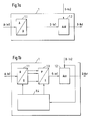
- the basic circuit 1 for the concentration of Data streams essentially from an A / D converter 1.1 and one Adder 1.2.
- This basic circuit has a first input for an in signal A-ln 1, called analog signal for short, in analog form, a second input for a data stream in digital form D-ln 2, briefly called digital data stream, and an output at which the Sum D-Out from the digitally converted analog signal D-ln 1 and the digital data stream D-ln 2 present at the second input Is made available.
- FIG. 1b shows further details of the basic circuit 1, namely additionally to the blocks 1.1, 1.2 shown in Fig. 1a, a parallel series converter 1.3 and a detector circuit 1.4 for the detection of a Synchronizing signal and to generate a derived Clock signal for sampling the analog signal A-ln 1.
- Basic circuit 1 First, the analog data stream A-ln 1 with the aid of the A / D converter 1.1 a present in parallel form Generated data stream that by means of the parallel series converter 1.3 in one serial digital data stream D-ln 1 is converted. This digital Data stream D-ln 1 is present at a first input of adder 1.2 whose second input is another digital data stream D-ln 2.
- Both digital data streams D-ln 1, D-ln 2 contain a sequence of data words. These are added digitally and form the sum D-Out Output signal of the basic circuit. From the at the second entrance of the Adders lying data stream D-ln 2, is using the Detector circuit 1.4 the respective word start and from it the sampling clock for the A / D converter 1.1 determined, and the synchronization signal for the Adders 1.2 formed such that the corresponding lowest value and most significant bits of the words of the data streams to be added in each case are synchronously fed to the adder 1.2.
- Number of inputs of the parallel series converter 1.3 greater than the number of the outputs of the A / D converter 1.1 to select an input of the parallel-series converter 1.3 for the supply of the synchronization signal to be able to use, and to add another in the serial data stream Reserve input for the overflow bit of adder 1.2.
- FIG. 2 shows an A / D converter / adder circuit made up of a number k Basic circuits 1, each with an input for an analog signal A-ln 1 ... A-ln k and an output for the sum D-Out of digital converted analog signals A-ln 1 ... A-ln k.
- the chain-like structure The circuit arrangement is characterized in that from the sum of the data streams also the synchronization signal for the following in the chain Basic circuit 1 is recovered, so that the Synchronization necessary information in the derailleur from Basic circuit 1 spreads to basic circuit 1 without a separate one Synchronizing signal must be transmitted, and thus compared to known prior art significantly facilitates synchronization becomes.
- each basic circuit 1 of the A / D converter / adder circuit different locations, for example on different floors of a building that can be arranged are not additional Circuits to compensate for differences in running time required.
- a serial transmission of data streams with high Transmission speeds are possible because of the realization of the A / D converter / adder circuit
- Semiconductor circuits in Si-Ge technology are used, which advantageously the power requirement is reduced compared to known parallel CMOS circuits, their complexity greater and their Processing speed is slower and an inexpensive Realization as a user-specific circuit.
- ASIC Application Specific Integrated Circuit.
- Fig. 3 shows a variant of the A / D converter / adder circuit with two Basic circuits 3 shown here from an A / D converter 3.1 and an adder 3.2. 3, it is possible to use the one shown in FIG Circuit structure to use even when processing the Data streams are not serial but in parallel.
- the most Output of the first basic circuit lying sum D-Outp 1 is considered Parallel information supplied to the second basic circuit and there to the analog / digitally converted data stream A-ln 2 added.
- an A / D converter / adder circuit is described, which are advantageously used in HFC networks for combined analog / digital conversion and concentration of signals and thus for more efficient Exploitation of transmission paths is suitable.
- a opto-electrical converter or an electro-optical converter to the A / D converter / adder circuit can be inexpensive user specific circuits for universal use in Realize broadband transmission systems.
Landscapes
- Engineering & Computer Science (AREA)
- Microelectronics & Electronic Packaging (AREA)
- Computer Networks & Wireless Communication (AREA)
- Signal Processing (AREA)
- Synchronisation In Digital Transmission Systems (AREA)
- Analogue/Digital Conversion (AREA)
- Optical Communication System (AREA)
- Dc Digital Transmission (AREA)
Abstract
Description
- Fig.1a, 1b
- ein Blockschaltbild einer Grundschaltung aus A/D-Wandler und digitalem Addierer,
- Fig. 2
- eine erfindungsgemäße Schaltungsanordnung zur Konzentration von Datenströmen,
- Fig. 3
- eine erste Variante der erfindungsgemäßen Schaltungsanordnung und
- Fig. 4
- eine zweite Variante der erfindungsgemäßen Schaltungsanordnung.
Claims (5)
- Verfahren zur Konzentration von Datenströmen in einem Breitbandübertragungssystem mit einer Grundschaltung (1) aus einem Analog/Digital-Wandler (1.1) und einem diesem nachgeschalteten Addierer (1.2),
dadurch gekennzeichnet, daß
einem ersten Eingang der Grundschaltung (1) ein analoges Signal (A-ln k) zugeführt wird, daß einem zweiten Eingang der Grundschaltung (1) ein digitaler Datenstrom (D-ln (k-1)) zugeführt wird und daß an dem Ausgang der Grundschaltung (1) eine Summe (D-Out k) aus dem digital gewandelten analogen Signal (D-ln k) und dem digitalen Datenstrom (D-In (k-1)) bereitgestellt wird, wobei aus dem digitalen Datenstrom (D-In (k-1)) mit Hilfe einer Detektorschaltung (1.4) ein Abtasttakt und ein Synchronisiersignal derart abgeleitet werden, daß entsprechend gleichwertige Bits des digital gewandelten analogen Signals (D-ln k) und des digitalen Datenstroms (D-In (k-1)) synchron dem Addierer (1.2) zugeführt werden, und daß die Summe (D-Out k) der Datenströme bedarfsweise für eine weitere Addition dem zweiten Eingang einer in einer Kettenschaltung nächstfolgenden Grundschaltung (1) zugeführt wird. - Verfahren nach Anspruch 1 dadurch gekennzeichnet, daß durch die Zusammenschaltung jeweils des Ausgangs einer Grundschaltung (1) mit dem zweiten Eingang einer weiteren Grundschaltung (1) eine Kettenschaltung gebildet wird, bei der den ersten Eingängen der Grundschaltung (1) die zu addierenden analogen Signale (A-ln k) zugeführt werden und daß an dem Ausgang der in der Kettenschaltung letzten Grundschaltung (1) die Summe (D-Out k) der zu addierenden analogen Signale (A-In k) als digitaler Datenstrom bereitgestellt wird.
- Verfahren nach Anspruch 1, dadurch gekennzeichnet, daß der ausgangsseitige digitale Datenstrom des Analog/Digital-Wandlers (1.1) einem Parallel-Serie-Wandler (1.3) zugeführt wird, an dessen Ausgang ein serieller Datenstrom (D-ln k) entsteht und die Addition des ersten und des zweiten Datenstroms (D-ln k, D-ln (k-1)) in serieller Form erfolgt.
- Verfahren nach Anspruch 1, dadurch gekennzeichnet, daß die Übertragung eines digitalen Datenstroms bit-parallel erfolgt.
- Schaltungsanordnung zur Konzentration von Signalen, die von unterschiedlichen Nachrichtenquellen herrühren, in einem Breitbandübertragungssystem, bei dem eine Nachrichtenquelle mit einem ersten Eingang einer Grundschaltung (1) aus einem Analog/Digital-Wandler (1.1) mit nachgeschaltetem Addierer(1.2) verbunden ist, dadurch gekennzeichnet, daß eine Anzahl k+1 Grundschaltungen (1) derart in Kette geschaltet sind, daß der Ausgang einer ersten Grundschaltung (1) mit einem zweiten Eingang einer zweiten Grundschaltung (1) verbunden ist, deren erster Eingang mit einer Nachrichtenquelle verbunden ist und daß der Ausgang der zweiten Grundschaltung (2) mit einem zweiten Eingang einer dritten Grundschaltung (1) verbunden ist, deren erster Eingang mit einer Nachrichtenquelle verbunden ist und daß der Ausgang einer k-ten Grundschaltung (1) mit einem zweiten Eingang einer (k+1)-ten Grundschaltung (1) verbunden ist und daß in jeder Grundschaltung (1) dem Analog/Digital-Wandler (1.1) und dem Addierer (1.2) eine Detektorschaltung (1.4) zugeordnet ist, deren Eingang mit dem zweiten Eingang der Grundschaltung (1) verbunden ist.
Applications Claiming Priority (2)
| Application Number | Priority Date | Filing Date | Title |
|---|---|---|---|
| DE1999112379 DE19912379A1 (de) | 1999-03-19 | 1999-03-19 | Verfahren und Schaltungsanordnung zur Konzentration von analogen Signalen zu einem digitalen Datenstrom in einem Breitbandübertragungssystem |
| DE19912379 | 1999-03-19 |
Publications (2)
| Publication Number | Publication Date |
|---|---|
| EP1039668A2 true EP1039668A2 (de) | 2000-09-27 |
| EP1039668A3 EP1039668A3 (de) | 2004-12-08 |
Family
ID=7901628
Family Applications (1)
| Application Number | Title | Priority Date | Filing Date |
|---|---|---|---|
| EP00440042A Withdrawn EP1039668A3 (de) | 1999-03-19 | 2000-02-09 | Verfahren und Schaltungsanordnung zur Konzentration von analogen Signalen zu einem digitalen Datenstrom in einem Breitbandübertragungssystem |
Country Status (2)
| Country | Link |
|---|---|
| EP (1) | EP1039668A3 (de) |
| DE (1) | DE19912379A1 (de) |
Family Cites Families (4)
| Publication number | Priority date | Publication date | Assignee | Title |
|---|---|---|---|---|
| GB1238658A (de) * | 1967-06-13 | 1971-07-07 | ||
| US5123015A (en) * | 1990-12-20 | 1992-06-16 | Hughes Aircraft Company | Daisy chain multiplexer |
| CA2121934A1 (en) * | 1993-06-14 | 1994-12-15 | Gordon Bremer | Simultaneous analog and digital communication with improved phase immunity |
| JP3120931B2 (ja) * | 1993-09-10 | 2000-12-25 | 松下電器産業株式会社 | 同期加算装置 |
-
1999
- 1999-03-19 DE DE1999112379 patent/DE19912379A1/de not_active Ceased
-
2000
- 2000-02-09 EP EP00440042A patent/EP1039668A3/de not_active Withdrawn
Also Published As
| Publication number | Publication date |
|---|---|
| DE19912379A1 (de) | 2000-10-12 |
| EP1039668A3 (de) | 2004-12-08 |
Similar Documents
| Publication | Publication Date | Title |
|---|---|---|
| DE69326303T2 (de) | Optischer Multiplexer-Demultiplexer mit Nyquistabtastrate | |
| DE68911134T2 (de) | Rahmen-demultiplexer für digitale signale hoher schrittgeschwindigkeit. | |
| DE69330729T2 (de) | Verfahren zur Symbolratenanpassung in einem Kommunikationsnetz | |
| EP1243061B1 (de) | Verfahren und anordnung zum erfassen und digitalen übertragen von analogen ausgangsmessgrössen mehrerer wandler | |
| EP0384918A1 (de) | Verfahren und Anordnung zum Anpassen eines Taktes an ein plesiochrones Datensignal und zu dessen Abtakten mit dem angepassten Takt | |
| WO1985003612A1 (fr) | Brouilleur a synchronisation automatique (scrambler) | |
| DE69411570T2 (de) | Optische decodierung für manchester-kodierte signale | |
| DE69326883T2 (de) | Optische verarbeitung in einem atm netz | |
| EP0164676A1 (de) | Selbstsynchronisierender Verwürfler | |
| EP1039668A2 (de) | Verfahren und Schaltungsanordnung zur Konzentration von analogen Signalen zu einem digitalen Datenstrom in einem Breitbandübertragungssystem | |
| EP0284106B1 (de) | Schaltungsanordnung zum Hinzufügen eines Dienstkanals für ein Nachrichtenübertragungssystem | |
| EP0680215A2 (de) | Verfahren zur Aufbereitung und Wiedergewinnung von Daten sowie Anordnungen hierzu | |
| EP0103163A2 (de) | Anordnung zum synchronen Demultiplexen eines Zeitmultiplexsignals | |
| DE3707243C2 (de) | ||
| EP0342530B1 (de) | Koppelfeld für digitale Audiosignale | |
| EP0972363B1 (de) | Verfahren zur übertragung von zusatzdatensignalen und einem nutzdatensignal über optische verbindungen | |
| DE4214375C2 (de) | Optisches Teilnehmeranschlußnetz mit Wellenlängenmultiplex und mehrdeutigem optischen Multiplexer/Demultiplexer | |
| DE60122841T2 (de) | Synchrones Datenübertragungssystem | |
| DE3318290A1 (de) | Telekommunikationssystem sowohl fuer stream-verkehr als auch fuer burst-verkehr | |
| DE3230271C2 (de) | ||
| DE2557830C3 (de) | Abzweigtechnik in digitalen Nachrichtennetzen | |
| EP0477131B1 (de) | Verfahren und Anordnungen zur Abtastratenwandlung | |
| DE3248624C2 (de) | ||
| EP1283612A1 (de) | OCDM-Detektionvorrichtung | |
| EP0408969B1 (de) | Einrichtung zum Laufzeitausgleich und zur Jitterbereinigung eines empfangenen Datensignals |
Legal Events
| Date | Code | Title | Description |
|---|---|---|---|
| PUAI | Public reference made under article 153(3) epc to a published international application that has entered the european phase |
Free format text: ORIGINAL CODE: 0009012 |
|
| AK | Designated contracting states |
Kind code of ref document: A2 Designated state(s): AT BE CH CY DE DK ES FI FR GB GR IE IT LI LU MC NL PT SE |
|
| AX | Request for extension of the european patent |
Free format text: AL;LT;LV;MK;RO;SI |
|
| 17P | Request for examination filed |
Effective date: 20040812 |
|
| PUAL | Search report despatched |
Free format text: ORIGINAL CODE: 0009013 |
|
| AK | Designated contracting states |
Kind code of ref document: A3 Designated state(s): AT BE CH CY DE DK ES FI FR GB GR IE IT LI LU MC NL PT SE |
|
| AX | Request for extension of the european patent |
Extension state: AL LT LV MK RO SI |
|
| RIC1 | Information provided on ipc code assigned before grant |
Ipc: 7H 04L 5/04 B Ipc: 7H 04J 15/00 A |
|
| AKX | Designation fees paid |
Designated state(s): AT BE CH CY DE DK ES FI FR GB GR IE IT LI LU MC NL PT SE |
|
| STAA | Information on the status of an ep patent application or granted ep patent |
Free format text: STATUS: THE APPLICATION IS DEEMED TO BE WITHDRAWN |
|
| 18D | Application deemed to be withdrawn |
Effective date: 20050609 |