EP1039515A2 - Source-drain contacts in MOS device and method of manufacturing the same - Google Patents
Source-drain contacts in MOS device and method of manufacturing the same Download PDFInfo
- Publication number
- EP1039515A2 EP1039515A2 EP00103846A EP00103846A EP1039515A2 EP 1039515 A2 EP1039515 A2 EP 1039515A2 EP 00103846 A EP00103846 A EP 00103846A EP 00103846 A EP00103846 A EP 00103846A EP 1039515 A2 EP1039515 A2 EP 1039515A2
- Authority
- EP
- European Patent Office
- Prior art keywords
- source
- spacers
- dielectric material
- vias
- forming
- Prior art date
- Legal status (The legal status is an assumption and is not a legal conclusion. Google has not performed a legal analysis and makes no representation as to the accuracy of the status listed.)
- Withdrawn
Links
Images





Classifications
-
- H—ELECTRICITY
- H10—SEMICONDUCTOR DEVICES; ELECTRIC SOLID-STATE DEVICES NOT OTHERWISE PROVIDED FOR
- H10W—GENERIC PACKAGES, INTERCONNECTIONS, CONNECTORS OR OTHER CONSTRUCTIONAL DETAILS OF DEVICES COVERED BY CLASS H10
- H10W20/00—Interconnections in chips, wafers or substrates
- H10W20/01—Manufacture or treatment
- H10W20/031—Manufacture or treatment of conductive parts of the interconnections
- H10W20/069—Manufacture or treatment of conductive parts of the interconnections by forming self-aligned vias or self-aligned contact plugs
-
- H—ELECTRICITY
- H10—SEMICONDUCTOR DEVICES; ELECTRIC SOLID-STATE DEVICES NOT OTHERWISE PROVIDED FOR
- H10W—GENERIC PACKAGES, INTERCONNECTIONS, CONNECTORS OR OTHER CONSTRUCTIONAL DETAILS OF DEVICES COVERED BY CLASS H10
- H10W20/00—Interconnections in chips, wafers or substrates
- H10W20/01—Manufacture or treatment
- H10W20/071—Manufacture or treatment of dielectric parts thereof
- H10W20/074—Manufacture or treatment of dielectric parts thereof of dielectric parts comprising thin functional dielectric layers, e.g. dielectric etch-stop, barrier, capping or liner layers
- H10W20/076—Manufacture or treatment of dielectric parts thereof of dielectric parts comprising thin functional dielectric layers, e.g. dielectric etch-stop, barrier, capping or liner layers in via holes or trenches
-
- H—ELECTRICITY
- H10—SEMICONDUCTOR DEVICES; ELECTRIC SOLID-STATE DEVICES NOT OTHERWISE PROVIDED FOR
- H10W—GENERIC PACKAGES, INTERCONNECTIONS, CONNECTORS OR OTHER CONSTRUCTIONAL DETAILS OF DEVICES COVERED BY CLASS H10
- H10W20/00—Interconnections in chips, wafers or substrates
- H10W20/40—Interconnections external to wafers or substrates, e.g. back-end-of-line [BEOL] metallisations or vias connecting to gate electrodes
Definitions
- This invention relates generally to semiconductor structures and manufacturing methods, and more particularly to structures and methods having reduced electrical short circuits between adjacent electrical contacts to the semiconductor.
- DRAM Dynamic Random Access Memory
- FIGS. 1, 2A and 3A a DRAM array 9 is shown at an early stage in the fabrication thereof.
- the array 9 is formed in a semiconductor body 10, here single crystal silicon.
- the array includes trench capacitors C as the storage elements.
- Each storage capacitor C is electrically connected to the drain D region of a CMOS transistor T associated with one of the DRAM cells in the array 9.
- the transistors T are formed in rows of active areas 11.
- the rows of active areas are electrically isolated from each other by shallow trench isolation (STI) regions 13.
- the array includes columns of wordline WL which are provide gate electrodes for the transistors T.
- a pair of adjacent transistors T in each one of the rows share a common source region S.
- the common source regions S are to be connected to bitlines of the DRAM array.
- gate electrode stack 15 of two adjacent transistors T in a common row thereof are formed on a thermally grown gate oxide layer 12, it being understood that dimensions in the FIGS. are not to scale.
- the array of DRAM cells includes a plurality of transistors T disposed in rows of electrically isolated active areas 11 of a surface of a semiconductor body 10.
- the transistors T have gate stacks 18 disposed in columns across the rows of active areas 11 and source/drain regions, here source regions S, it being understood that the terms source and drain may be used interchangeably, in the regions of the active areas 11 between adjacent pairs of the columns of gate stacks 18.
- the gate oxide layer 12 is disposed over the entire surface of the silicon body 10.
- the gate electrode stack 15 includes a bottom layer 14 of doped polycrystalline silicon, a middle layer 16 of tungsten suicide, and a cap 18 of silicon nitride, as well as silicon nitride sidewall spacers 20.
- a layer 32 of silicon nitride is formed over the surface of the structure shown in FIGS. 1, 2A and 3A.
- a pre-metal dielectric layer 34 typically borophosphosilicate glass (BPSG)
- CMP chemical mechanical polishing
- a film 36 of doped or undoped silicon oxide is finally deposited as a blanket layer to tune the distance to the next level of metalization.
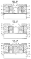
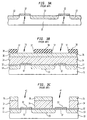
- a photoresist mask 38 is applied and patterned with windows 39, as shown in FIGS. 2B and 3B. It is noted that the width W of the windows 39 are slightly wider than the gap between the gate electrode stacks 15 (FIG. 2B).
- the portions of the oxide film 36, BPSG layer 34 stack exposed by the windows 39 are etched with a dry etch (e.g., anisotropic RIE) which removes silicon dioxide in film 36 and BPSG in layer 34 at a substantially higher etch rate than the etch rate of the photoresist mask 38 or the silicon nitride 32.
- a dry etch e.g., anisotropic RIE
- FIGS. 2C and 3C The resulting structure, after the mask 38 is removed, is shown in FIGS. 2C and 3C.
- the contact openings, or vias 41 formed by the etching process are self aligned along the rows of active regions 11 (FIG. 1) , as shown in FIG. 2C because of the silicon nitride 32; however, the openings 41 are not self-aligned in the orthogonal direction (i.e., a direction parallel to the columns
- the photoresist mask 38 is stripped, the silicon nitride layer 32 is etched away, with the much thicker silicon nitride spacers 20 being slightly eroded, to produce the structure shown in FIGS. 2D and 3D.
- the portions of the gate oxide 12 between the gate electrode stacks 14, must be removed.
- a dilute hydrofluoric acid (HF) etch dip is used to: (1) remove any residual material which may remain from the dry etch; and (2) to ensure that the silicon dioxide layer between the gate electrode stacks 14 is totally removed (i.e., the silicon 10 is exposed).
- the HF etch etches silicon dioxide at a greater etch rate than silicon nitride.
- FIGS. 2E and 3E The resulting structure is shown in FIGS. 2E and 3E. It is noted that while the silicon nitride spacers provide protection to the gate electrode stacks 14 during the dilute hydrofluoric acid dip, the dip eats into (i.e., etches-out) the portions of the BPSG layer 14 and silicon dioxide 36 along the perpendicular direction (i.e., the direction parallel to the columns of wordlines) because the is no silicon nitride spacers, as indicated in FIGS. 3D and 3E. This etch-out of the BPSG is increased as the amount of boron in the BPSG is increases to accommodate the reflow-temperature requirements of small geometry devices. Thus, the width W' of the BPSG layer 34 and silicon dioxide is significantly reduced.
- a layer 40 of conductive material 40 is applied to the surface of the structures shown in FIGS. 2E and 3E and then planarized to produce the bitline contacts to the source regions S (FIG. 2F). It is noted, however, in FIG. 3F, that the reduction in the width W' (FIG. 35) increases the probably of an electrical short between adjacent bitlines, BLs, as shown in FIG. 3F.
- the conductive material 40 is doped polycrystalline silicon (i.e., poly), there is no need for implantation provided dopant in the silicon 10, i.e., with doped poly, there is no need for dopant in the silicon to provide an ohmic contact between the doped poly and the silicon.
- the conductive material 40 is a metal, however, dopant is required in the silicon 10 in order to achieve ohmic contact.
- ion implantation to provide these doped regions, however, requires a thermal anneal step to activate the implanted ions. The thermal anneal also, however, diffuses the dopant which may have an adverse effect on device characteristics with small devices.
- polycrystalline silicon fills high aspect rations very well; however, it has a disadvantage over metal because of the relatively high resistance of doped poly compared to that of metal.
- a method for forming a semiconductor structure. The method includes: forming a first dielectric on a semiconductor body; forming a second dielectric over the first dielectric; forming a third dielectric over the second dielectric; forming a via through a selected portion of the third dielectric to expose an underlying portion of the second dielectric; forming a via through the exposed portion of the second dielectric to expose an underling portion of the first dielectric; forming a spacer on sidewalls of the vias, such spacer being of a material which etches to an etch at an etch rate substantially lower than the etch rate of the first dielectric to said etch; and, bringing the etch into contact with the spacer and the exposed portion of the first dielectric to remove the exposed portion of the first dielectric.
- a method for forming source/drain contacts to source/drain regions of an array of transistors.
- the method includes providing a semiconductor body with a gate oxide layer over the surface of the semiconductor body.
- the gate oxide layer extends over active areas in the semiconductor body.
- Gate stacks are provided on the gate oxide layer in columns across the rows of the active areas.
- a dielectric material is deposited over the surface of the provided semiconductor body. Vias are etched through the dielectric material over source/drain regions provided in portions of the active area between the columns of gate stacks. First portions of sidewalls of such vias are formed over portions of adjacent columns of the gate stacks and second portions of the sidewalls of such vias are formed between adjacent columns of the gate stacks.
- the vias expose portions of the gate oxide layer over the source/drain regions.
- Source/drain contacts are formed in the vias, such formation comprising: forming spacers on the sidewalls of the regions of dielectric material; exposing the exposed portions of the gate oxide to an etch to remove such exposed portions of the gate oxide layer, such etch etching the gate oxide at a substantially higher etch rate that to the spacers; and, forming conductive materials on the spacers and in contact with the source/drain regions.
- the columns of gate stacks have silicon nitride sidewall spacers.
- the dielectric material includes an oxide.
- the spacers are a material different from the oxide and is resistant to the etch used to etch the oxide.
- the vias thus expose the portions of the gate oxide and absent the spacers, the dielectric material, which is also an oxide.
- the spacers are on the sidewalls of the oxide dielectric material and are not etched by the etch used to remove the exposed portions of the gate oxide. Thus, there is no etch-out of the dielectric material. Consequently, the spacers prevent etching of the dielectric material between adjacent source/drain contacts which are disposed between a pair of adjacent columns of the gate stacks thereby enabling the use of boron doped oxide dielectric material.
- a semiconductor structure having a plurality of transistors disposed in rows of electrically isolated active areas of a surface of a semiconductor body.
- the transistors have gate stacks disposed in columns across the rows of active areas and source/drain regions in the active areas between adjacent pairs of the columns of gate stacks.
- a dielectric material is disposed over the surface of the semiconductor body.
- the dielectric material has vias therethrough disposed over the source/drain regions. First portions of the sidewalls of such vias are disposed over portions of adjacent columns of the gate stacks and second portions of the sidewalls of such vias are disposed between adjacent columns of the gate stacks.
- Source/drain contacts are disposed in the vias.
- the source/drain contacts include spacers disposed on the sidewalls of the regions of dielectric material and conductive materials disposed on the spacers and in contact with the source/drain regions.
- the spacers provide a shield to ion implanted particles used to provide a doped, ohmic contact for the source/drain region when a metal conductor is used for the source/drain contact.
- the spacers are a conductive material to prevent increased resistive to the conductive material in the via.
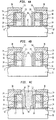
- a conformal layer of a conductive, nonhydrofluoric acid etchable material for example, doped polycrystalline silicon is deposited over the structure shown in FIGS. 2D and 3D.
- An anisotropic e.g. Reactive Ion Etch (RIE)
- RIE Reactive Ion Etch
- spacers 50 can also be any other conductive material provided that it cannot be etched in buffered hydrofluoric acid or dilute hydrofluoric acid, and that it can take subsequent thermal treatments. It should also adhere to the underlying dielectric films, have acceptable step coverage, and be deposited with sufficient uniformity as a thin film. Other materials include doped and undoped polycrystalline silicon, or sputtered amorphous silicon.
- FIGS. 4B and 5B It is noted that there is no etch-out of the BPSG 34 and silicon dioxide 36 (as shown in FIG. 3E) because here these layers 34, 36 are shielded from the hydrofluoric acid dip by the spacers 50.
- the resulting structure is shown in FIGS. 4B and 5B.
- a conductive material 54 is deposited over the surface of the structure shown in FIG.
- the material 54 in FIGS. 4C and 4D is doped polycrystalline silicon. It is noted that no doping is required in the underlying silicon 10. Further, because the spacer 50 is also conductive, they become part of the conductive bitline and the narrowing of the contact hole because of the spacer 50 does not reduce the area provided for the electrical contact to the silicon 10.
- a metal is used instead of using a polycrystalline silicon material 54 . More particularly, after forming the structure shown in FIG. 4B, the structure is subjected to ion implantation, the ions implanted in the exposed silicon 10 being indicated by x's in FIG. 6A. It is noted that the spacers 50 provide a shielding effect to the implantation so that the ions are spaced by a distance Z from the edges of the silicon nitride spacers 20.
- tungsten is to be used for the conductive material 54. However, because tungsten does not adhere to dielectrics well, a liner 58 of titanium nitride is first deposited using physical vapor deposition.
- Step coverage is limited for the physical vapor deposition of the titanium nitride liner 58 in the high aspect ratio vias. It is noted that, here, the titanium nitride liner 58 need not reach to the bottom of the via; instead, the final tungsten 54 adheres to the poly sidewall spacers 52 and will fill the via contact area.
- the structure is then annealed to activate the ions x and to diffused to dopant and provide doped, ohmic contact region 60.
Landscapes
- Internal Circuitry In Semiconductor Integrated Circuit Devices (AREA)
- Electrodes Of Semiconductors (AREA)
- Semiconductor Memories (AREA)
- Insulated Gate Type Field-Effect Transistor (AREA)
Abstract
Description
Claims (53)
- A method for forming a semiconductor structure, comprising:forming a first dielectric on a semiconductor body;forming a second dielectric over the first dielectric;forming a third dielectric over the second dielectric;forming a via through a selected portion of the third dielectric to expose an underlying portion of the second dielectric;forming a via through the exposed portion of the second dielectric to expose an underling portion of the first dielectric;forming a spacer on sidewalls of the vias, such spacer being of a material which etches to an etch at an etch rate substantially lower than the etch rate of the first dielectric to said etch;bringing the etch into contact with the spacer and the exposed portion of the first dielectric to remove the exposed portion of the first dielectric.
- The method recited in claim 1 wherein the first dielectric comprises silicon dioxide.
- The method recited in claim 2 wherein the third material comprises boron doped glass.
- The method recited in claim 2 wherein the second dielectric comprises silicon nitride.
- The method recited in claim 4 wherein the third dielectric comprises boron doped glass.
- The method recited in claim 5 wherein the spacer comprises silicon.
- The method recited in claim 6 including forming an electrical contact through the spacer via, such contact being in contact with the spacer and the exposed portion of the semiconductor body.
- The method recited in claim 7 including forming the contact in ohmic contact with the exposed portion of the semiconductor body.
- The method recited in claim 1 including forming an electrical contact through the spacer via, such contact being in contact with the spacer and the exposed portion of the semiconductor body.
- The method recited in claim 9 including forming the contact in ohmic contact with the exposed portion of the semiconductor body.
- A method is provided for forming source/drain contacts to source/drain regions of an array of transistors, such method comprising:(a) providing a semiconductor body with a gate oxide layer over the surface of the semiconductor body, such gate oxide layer extending over active areas in the semiconductor body, such body having gate stacks on the gate oxide layer in columns across the rows of active areas, such gate oxide extending over source/drain regions in portions the active ares;(b) forming a dielectric material over the surface of the provided semiconductor body;(c) etching vias through the dielectric material over source/drain regions in portions of the active areas between the columns of gate stacks, first portions of sidewalls of such vias being formed over portions of adjacent columns of the gate stacks and second portions of the sidewalls of such vias being formed between adjacent columns of the gate stacks, such vias exposing the portions of the gate oxide layer over the source/drain regions;(d) forming source/drain contacts in the vias, such formation comprising:(i) forming spacers on the sidewalls of the regions of dielectric material;(ii) exposing the exposed portions of the gate oxide to an etch to remove such exposed portions of the gate oxide layer, such etch etching the gate oxide at a substantially higher etch rate than to the spacers;and, (iii) forming conductive materials on the spacers and in contact with the source/drain regions.
- The method recited in claim 11 wherein the columns of gate stacks are provided with silicon nitride sidewall spacers.
- The method recited in claim 12 wherein the dielectric material includes an oxide.
- The method recited in claim 13 wherein the spacers comprise a material different from the oxide and is resistant to the etch used to etch the oxide.
- The method recited in claim 11 including the step of implanting ions into the source/drain region with the spacers providing a shield to the ion implantation.
- A semiconductor structure, comprising:a plurality of rows of electrically isolated active areas of a surface of a semiconductor body;gate stacks disposed in columns across the rows of active areas;source/drain regions in the active areas between adjacent pairs of the columns of gate stacks;a dielectric material disposed over the surface of the semiconductor body, the dielectric material having vias therethrough disposed over the source/drain regions, first portions of the sidewalls of such vias being disposed over portions of adjacent columns of the gate stacks and second portions of the sidewalls of such vias being disposed between adjacent columns of the gate stacks;source/drain contacts disposed in the vias, such contacts comprising:spacers disposed on the sidewalls of the regions of dielectric material; andconductive materials disposed on the spacers and in contact with the source/drain regions.
- The structure recited in claim 16 wherein the spacers are a conductive material.
- An semiconductor structure, comprising:(a) a plurality of rows of electrically isolated active areas of a surface of a semiconductor body;(b) gate stacks disposed in columns across the rows of active areas;(c) source/drain regions in the active areas between adjacent pairs of the columns of gate stacks;(d) dielectric material disposed over the surface of the semiconductor body, such material having vias therethrough disposed over the source/drain regions, first portions of sidewalls of such vias being disposed over portions of adjacent columns of the gate stacks and second portions of the sidewalls of such vias being disposed between adjacent columns of the gate stacks;(e) source/drain contacts disposed in the vias, such contacts comprising:(i) spacers disposed on the sidewalls of the regions of dielectric material; and(ii) conductive materials disposed on the spacers and in contact with the source/drain regions.
- The semiconductor structure recited in claim 18 wherein:the semiconductor body is silicon;the dielectric material comprises an oxide; andthe spacers comprise silicon.
- The semiconductor structure recited in claim 19 wherein the dielectric material comprises boron doped glass.
- The semiconductor structure recited in claim 18 wherein the spacers are electrically conductive.
- The semiconductor structure recited in claim 21 wherein:the semiconductor body is silicon;the dielectric material comprises an oxide; and
the spacers comprise silicon. - The semiconductor structure recited in claim 22 wherein the dielectric material comprises boron doped glass.
- The semiconductor structure recited in claim 18 wherein the conductive material is doped silicon.
- The semiconductor structure recited in claim 18 wherein the conductive material is a metal in ohmic contact with the source/drain region.
- The semiconductor structure recited in claim 24 wherein the dielectric material comprises boron doped glass.
- The semiconductor structure recited in claim 26 wherein the spacers are electrically conductive.
- The semiconductor structure recited in claim 25 wherein the dielectric material comprises boron doped glass.
- The semiconductor structure recited in claim 28 wherein the spacers are electrically conductive.
- An array of memory cells, such cells comprising:(a) storage capacitors;(b) transistors, disposed in rows of electrically isolated active areas of a surface of a semiconductor body, such transistors being electrically connected to the capacitors, such transistors having source/drain regions in the active areas and gate stacks disposed in columns;(c) dielectric material disposed over the surface of the semiconductor body, such dielectric material having vias over the source/drain regions;(d) source/drain contacts disposed in the vias, such contacts comprising:(i) spacers disposed on sidewalls of the vias; and(ii) conductive material disposed on the spacers and in contact with the source/drain regions.
- The array recited in claim 30 wherein:the semiconductor body is silicon;the dielectric material comprises an oxide; and
the spacers comprise silicon. - The array recited in claim 31 wherein the dielectric material comprises boron doped glass.
- The array recited in claim 32 wherein the spacers are electrically conductive.
- The array recited in claim 29 wherein:the semiconductor body is silicon;the dielectric material comprises an oxide; and
the spacers comprise silicon. - The array recited in claim 34 wherein the dielectric material comprises boron doped glass.
- A method for forming a semiconductor structure, comprising:(a) providing a plurality of electrically isolated active areas of a surface of a semiconductor body, such body having gate stacks disposed in columns across the rows of active areas and source/drain regions in the active areas between adjacent pairs of the columns of gate stacks, such semiconductor body have a gate oxide layer on the surface of the active areas of the semiconductor body under the gate stacks and over the source/drain regions;(b) forming a dielectric material over the surface of the semiconductor body;(c) forming having vias there portions of the dielectric material disposed over the source/drain regions, first portions of sidewalls of such vias being over portions of adjacent columns of the gate stacks and second portions of the sidewalls of such vias being between adjacent columns of the gate stacks, such vias exposing portions of the gate oxide disposed over the source/drain regions;(d) forming source/drain contacts in the vias, comprising:(i) forming spacers on the sidewalls of the regions of dielectric material;(ii) bringing an etch into contact with the exposed portions of the gate oxide; and(iii) forming conductive materials on the spacers and in contact with the source/drain regions.
- The method recited in claim 36 wherein:the semiconductor body is silicon;the dielectric material comprises an oxide; andthe spacers comprise silicon.
- The method recited in claim 37 wherein the dielectric material comprises boron doped glass.
- The method recited in claim 36 wherein the spacers are electrically conductive.
- The method recited in claim 39 wherein:the semiconductor body is silicon;the dielectric material comprises an oxide; and
the spacers comprise silicon. - The semiconductor structure recited in claim 40 wherein the dielectric material comprises boron doped glass.
- The semiconductor structure recited in claim 36 wherein the conductive material is doped silicon.
- The semiconductor structure recited in claim 36 wherein the conductive material is a metal in ohmic contact with the source/drain region.
- The semiconductor structure recited in claim 41 wherein the dielectric material comprises boron doped glass.
- The semiconductor structure recited in claim 43 wherein the spacers are electrically conductive.
- The semiconductor structure recited in claim 45 wherein the dielectric material comprises boron doped glass.
- The semiconductor structure recited in claim 46 wherein the spacers are electrically conductive.
- An method for forming an array of memory cells, comprising:(a) providing storage capacitors electrically connected to transistors with such transistors disposed in rows of electrically isolated active areas of a surface of a semiconductor body, such transistors having source/drain regions in the active areas and gate stacks disposed in columns;(b) forming a dielectric material over the surface of the semiconductor body;(c) forming vias in the dielectric material over the source/drain regions;(d) forming source/drain contacts in the vias, comprising:(i) forming spacers on sidewalls of the vias; and(ii) forming conductive material on the spacers and in contact with the source/drain regions.
- The method recited in claim 48 wherein:the semiconductor body is silicon;the dielectric material comprises an oxide; and
the spacers comprise silicon. - The method recited in claim 49 wherein the dielectric material comprises boron doped glass.
- The method recited in claim 50 wherein the spacers are electrically conductive.
- The method recited in claim 47 wherein:the semiconductor body is silicon;the dielectric material comprises an oxide; and
the spacers comprise silicon. - The method recited in claim 52 wherein the dielectric material comprises boron doped glass.
Applications Claiming Priority (2)
| Application Number | Priority Date | Filing Date | Title |
|---|---|---|---|
| US09/276,027 US6245629B1 (en) | 1999-03-25 | 1999-03-25 | Semiconductor structures and manufacturing methods |
| US276027 | 1999-03-25 |
Publications (2)
| Publication Number | Publication Date |
|---|---|
| EP1039515A2 true EP1039515A2 (en) | 2000-09-27 |
| EP1039515A3 EP1039515A3 (en) | 2005-04-27 |
Family
ID=23054840
Family Applications (1)
| Application Number | Title | Priority Date | Filing Date |
|---|---|---|---|
| EP00103846A Withdrawn EP1039515A3 (en) | 1999-03-25 | 2000-02-24 | Source-drain contacts in MOS device and method of manufacturing the same |
Country Status (6)
| Country | Link |
|---|---|
| US (1) | US6245629B1 (en) |
| EP (1) | EP1039515A3 (en) |
| JP (1) | JP4950373B2 (en) |
| KR (1) | KR20000076942A (en) |
| CN (1) | CN1171285C (en) |
| TW (1) | TW476999B (en) |
Families Citing this family (7)
| Publication number | Priority date | Publication date | Assignee | Title |
|---|---|---|---|---|
| KR100331861B1 (en) * | 2000-07-21 | 2002-04-09 | Hynix Semiconductor Inc | Method for fabricating gate electrode of semiconductor device |
| FR2822293B1 (en) * | 2001-03-13 | 2007-03-23 | Nat Inst Of Advanced Ind Scien | FIELD EFFECT TRANSISTOR AND DOUBLE GRID, INTEGRATED CIRCUIT COMPRISING THIS TRANSISTOR, AND METHOD OF MANUFACTURING THE SAME |
| KR100755627B1 (en) * | 2001-12-05 | 2007-09-04 | 매그나칩 반도체 유한회사 | Capacitor Manufacturing Method of Semiconductor Device |
| KR100457038B1 (en) | 2002-09-24 | 2004-11-10 | 삼성전자주식회사 | Method for forming a self align contact in semiconductor device and manufacturing a semiconductor device using for same |
| US6909152B2 (en) * | 2002-11-14 | 2005-06-21 | Infineon Technologies, Ag | High density DRAM with reduced peripheral device area and method of manufacture |
| US20060070204A1 (en) * | 2004-10-05 | 2006-04-06 | Tacony Corporation | Flow control valve system for an upright vacuum cleaner with a cleaning hose |
| US20090218627A1 (en) * | 2008-02-28 | 2009-09-03 | International Business Machines Corporation | Field effect device structure including self-aligned spacer shaped contact |
Family Cites Families (13)
| Publication number | Priority date | Publication date | Assignee | Title |
|---|---|---|---|---|
| US5256583A (en) * | 1986-03-21 | 1993-10-26 | Advanced Power Technology, Inc. | Mask surrogate semiconductor process with polysilicon gate protection |
| JPH0294564A (en) * | 1988-09-30 | 1990-04-05 | Toshiba Corp | Manufacture of semiconductor device |
| KR940006682B1 (en) * | 1991-10-17 | 1994-07-25 | 삼성전자 주식회사 | Manufacturing Method of Semiconductor Memory Device |
| EP0558304B1 (en) * | 1992-02-28 | 2000-01-19 | STMicroelectronics, Inc. | Method of forming submicron contacts |
| US5317192A (en) * | 1992-05-06 | 1994-05-31 | Sgs-Thomson Microelectronics, Inc. | Semiconductor contact via structure having amorphous silicon side walls |
| US5384281A (en) * | 1992-12-29 | 1995-01-24 | International Business Machines Corporation | Non-conformal and oxidizable etch stops for submicron features |
| JPH0722346A (en) * | 1993-07-02 | 1995-01-24 | Mitsubishi Electric Corp | Semiconductor device and manufacturing method thereof |
| JP3795634B2 (en) * | 1996-06-19 | 2006-07-12 | 株式会社東芝 | Manufacturing method of semiconductor device |
| JP3614267B2 (en) * | 1997-02-05 | 2005-01-26 | 株式会社ルネサステクノロジ | Manufacturing method of semiconductor integrated circuit device |
| JPH10261713A (en) * | 1997-03-19 | 1998-09-29 | Sony Corp | Method for manufacturing semiconductor device |
| JPH10321724A (en) * | 1997-03-19 | 1998-12-04 | Fujitsu Ltd | Semiconductor device and manufacturing method thereof |
| JPH1117149A (en) * | 1997-04-30 | 1999-01-22 | Fujitsu Ltd | Semiconductor device and manufacturing method thereof |
| US6103456A (en) * | 1998-07-22 | 2000-08-15 | Siemens Aktiengesellschaft | Prevention of photoresist poisoning from dielectric antireflective coating in semiconductor fabrication |
-
1999
- 1999-03-25 US US09/276,027 patent/US6245629B1/en not_active Expired - Lifetime
-
2000
- 2000-02-24 EP EP00103846A patent/EP1039515A3/en not_active Withdrawn
- 2000-03-24 KR KR1020000014995A patent/KR20000076942A/en not_active Withdrawn
- 2000-03-27 CN CNB00104804XA patent/CN1171285C/en not_active Expired - Lifetime
- 2000-03-27 JP JP2000086588A patent/JP4950373B2/en not_active Expired - Fee Related
- 2000-08-15 TW TW089105343A patent/TW476999B/en not_active IP Right Cessation
Also Published As
| Publication number | Publication date |
|---|---|
| JP4950373B2 (en) | 2012-06-13 |
| CN1288251A (en) | 2001-03-21 |
| JP2000340655A (en) | 2000-12-08 |
| EP1039515A3 (en) | 2005-04-27 |
| TW476999B (en) | 2002-02-21 |
| CN1171285C (en) | 2004-10-13 |
| KR20000076942A (en) | 2000-12-26 |
| US6245629B1 (en) | 2001-06-12 |
Similar Documents
| Publication | Publication Date | Title |
|---|---|---|
| US6258649B1 (en) | Semiconductor integrated circuit device and method of manufacturing the same | |
| KR100320332B1 (en) | Semiconductor device and manufacturing method thereof | |
| US6555450B2 (en) | Contact forming method for semiconductor device | |
| JP2827728B2 (en) | Semiconductor memory device and method of manufacturing the same | |
| US5874359A (en) | Small contacts for ultra large scale integration semiconductor devices without separation ground rule | |
| US5468670A (en) | Method for fabricating a semiconductor memory device having a stacked capacitor cell | |
| US6703306B2 (en) | Methods of fabricating integrated circuit memories including titanium nitride bit lines | |
| US5523542A (en) | Method for making dynamic random access memory cell capacitor | |
| US6333233B1 (en) | Semiconductor device with self-aligned contact and its manufacture | |
| US7928515B2 (en) | Semiconductor device and manufacturing method of the semiconductor device | |
| US20010009805A1 (en) | Borderless contact structure and method of forming the same | |
| US6391756B1 (en) | Semiconductor processing methods of forming contact openings | |
| US5536673A (en) | Method for making dynamic random access memory (DRAM) cells having large capacitor electrode plates for increased capacitance | |
| US6245629B1 (en) | Semiconductor structures and manufacturing methods | |
| KR100647481B1 (en) | Method for manufacturing semiconductor device using self-aligned contact process | |
| HK1037270A (en) | Semiconductor structures and manufacturing methods | |
| KR19980081869A (en) | Semiconductor device and manufacturing method thereof | |
| KR20010064326A (en) | Method for forming MOS transistor in semiconductor device | |
| KR20030000668A (en) | Method for forming a contact hole of a semiconductor device | |
| KR20000067132A (en) | Method of manufacturing contact semiconductor device |
Legal Events
| Date | Code | Title | Description |
|---|---|---|---|
| PUAI | Public reference made under article 153(3) epc to a published international application that has entered the european phase |
Free format text: ORIGINAL CODE: 0009012 |
|
| AK | Designated contracting states |
Kind code of ref document: A2 Designated state(s): AT BE CH CY DE DK ES FI FR GB GR IE IT LI LU MC NL PT SE |
|
| AX | Request for extension of the european patent |
Free format text: AL;LT;LV;MK;RO;SI |
|
| PUAL | Search report despatched |
Free format text: ORIGINAL CODE: 0009013 |
|
| AK | Designated contracting states |
Kind code of ref document: A3 Designated state(s): AT BE CH CY DE DK ES FI FR GB GR IE IT LI LU MC NL PT SE |
|
| AX | Request for extension of the european patent |
Extension state: AL LT LV MK RO SI |
|
| 17P | Request for examination filed |
Effective date: 20050707 |
|
| RAP1 | Party data changed (applicant data changed or rights of an application transferred) |
Owner name: INFINEON TECHNOLOGIES AG |
|
| AKX | Designation fees paid |
Designated state(s): DE FR GB IE IT NL |
|
| 17Q | First examination report despatched |
Effective date: 20060821 |
|
| STAA | Information on the status of an ep patent application or granted ep patent |
Free format text: STATUS: THE APPLICATION IS DEEMED TO BE WITHDRAWN |
|
| 18D | Application deemed to be withdrawn |
Effective date: 20080605 |