EP1035565A2 - Method of manufacturing semiconductor device including high-temperature heat treatment - Google Patents
Method of manufacturing semiconductor device including high-temperature heat treatment Download PDFInfo
- Publication number
- EP1035565A2 EP1035565A2 EP00301383A EP00301383A EP1035565A2 EP 1035565 A2 EP1035565 A2 EP 1035565A2 EP 00301383 A EP00301383 A EP 00301383A EP 00301383 A EP00301383 A EP 00301383A EP 1035565 A2 EP1035565 A2 EP 1035565A2
- Authority
- EP
- European Patent Office
- Prior art keywords
- heat treatment
- temperature heat
- temperature
- crystal defects
- semiconductor device
- Prior art date
- Legal status (The legal status is an assumption and is not a legal conclusion. Google has not performed a legal analysis and makes no representation as to the accuracy of the status listed.)
- Withdrawn
Links
- 238000010438 heat treatment Methods 0.000 title claims abstract description 176
- 239000004065 semiconductor Substances 0.000 title claims abstract description 68
- 238000004519 manufacturing process Methods 0.000 title claims abstract description 44
- 230000007547 defect Effects 0.000 claims abstract description 82
- 239000013078 crystal Substances 0.000 claims abstract description 79
- 239000012535 impurity Substances 0.000 claims abstract description 73
- 238000005468 ion implantation Methods 0.000 claims abstract description 39
- 239000000758 substrate Substances 0.000 claims abstract description 29
- 150000001875 compounds Chemical class 0.000 claims description 33
- 229910052751 metal Inorganic materials 0.000 claims description 17
- 239000002184 metal Substances 0.000 claims description 17
- 230000003213 activating effect Effects 0.000 claims description 11
- 230000004913 activation Effects 0.000 claims description 7
- 238000011084 recovery Methods 0.000 claims description 6
- 239000010408 film Substances 0.000 description 35
- 238000004151 rapid thermal annealing Methods 0.000 description 31
- 239000010936 titanium Substances 0.000 description 14
- 229910052719 titanium Inorganic materials 0.000 description 13
- RTAQQCXQSZGOHL-UHFFFAOYSA-N Titanium Chemical compound [Ti] RTAQQCXQSZGOHL-UHFFFAOYSA-N 0.000 description 12
- 238000000034 method Methods 0.000 description 8
- 229910021341 titanium silicide Inorganic materials 0.000 description 8
- 230000005669 field effect Effects 0.000 description 5
- MHAJPDPJQMAIIY-UHFFFAOYSA-N Hydrogen peroxide Chemical compound OO MHAJPDPJQMAIIY-UHFFFAOYSA-N 0.000 description 4
- 238000009792 diffusion process Methods 0.000 description 4
- 239000012212 insulator Substances 0.000 description 4
- 238000002955 isolation Methods 0.000 description 4
- 125000006850 spacer group Chemical group 0.000 description 4
- 229910021419 crystalline silicon Inorganic materials 0.000 description 3
- 229910052736 halogen Inorganic materials 0.000 description 3
- 150000002367 halogens Chemical class 0.000 description 3
- 230000003071 parasitic effect Effects 0.000 description 3
- 229910021332 silicide Inorganic materials 0.000 description 3
- FVBUAEGBCNSCDD-UHFFFAOYSA-N silicide(4-) Chemical compound [Si-4] FVBUAEGBCNSCDD-UHFFFAOYSA-N 0.000 description 3
- VHUUQVKOLVNVRT-UHFFFAOYSA-N Ammonium hydroxide Chemical compound [NH4+].[OH-] VHUUQVKOLVNVRT-UHFFFAOYSA-N 0.000 description 2
- PXHVJJICTQNCMI-UHFFFAOYSA-N Nickel Chemical compound [Ni] PXHVJJICTQNCMI-UHFFFAOYSA-N 0.000 description 2
- 229910008486 TiSix Inorganic materials 0.000 description 2
- 238000000137 annealing Methods 0.000 description 2
- 229910052796 boron Inorganic materials 0.000 description 2
- 238000005530 etching Methods 0.000 description 2
- 238000002347 injection Methods 0.000 description 2
- 239000007924 injection Substances 0.000 description 2
- 239000011259 mixed solution Substances 0.000 description 2
- BASFCYQUMIYNBI-UHFFFAOYSA-N platinum Chemical compound [Pt] BASFCYQUMIYNBI-UHFFFAOYSA-N 0.000 description 2
- ZOXJGFHDIHLPTG-UHFFFAOYSA-N Boron Chemical compound [B] ZOXJGFHDIHLPTG-UHFFFAOYSA-N 0.000 description 1
- VYZAMTAEIAYCRO-UHFFFAOYSA-N Chromium Chemical compound [Cr] VYZAMTAEIAYCRO-UHFFFAOYSA-N 0.000 description 1
- ZOKXTWBITQBERF-UHFFFAOYSA-N Molybdenum Chemical compound [Mo] ZOKXTWBITQBERF-UHFFFAOYSA-N 0.000 description 1
- XUIMIQQOPSSXEZ-UHFFFAOYSA-N Silicon Chemical compound [Si] XUIMIQQOPSSXEZ-UHFFFAOYSA-N 0.000 description 1
- 229910008479 TiSi2 Inorganic materials 0.000 description 1
- NRTOMJZYCJJWKI-UHFFFAOYSA-N Titanium nitride Chemical compound [Ti]#N NRTOMJZYCJJWKI-UHFFFAOYSA-N 0.000 description 1
- QCWXUUIWCKQGHC-UHFFFAOYSA-N Zirconium Chemical compound [Zr] QCWXUUIWCKQGHC-UHFFFAOYSA-N 0.000 description 1
- QGZKDVFQNNGYKY-UHFFFAOYSA-N ammonia Natural products N QGZKDVFQNNGYKY-UHFFFAOYSA-N 0.000 description 1
- DFJQEGUNXWZVAH-UHFFFAOYSA-N bis($l^{2}-silanylidene)titanium Chemical group [Si]=[Ti]=[Si] DFJQEGUNXWZVAH-UHFFFAOYSA-N 0.000 description 1
- 150000001638 boron Chemical class 0.000 description 1
- 229910052804 chromium Inorganic materials 0.000 description 1
- 239000011651 chromium Substances 0.000 description 1
- 229910017052 cobalt Inorganic materials 0.000 description 1
- 239000010941 cobalt Substances 0.000 description 1
- GUTLYIVDDKVIGB-UHFFFAOYSA-N cobalt atom Chemical compound [Co] GUTLYIVDDKVIGB-UHFFFAOYSA-N 0.000 description 1
- 230000000295 complement effect Effects 0.000 description 1
- 239000004020 conductor Substances 0.000 description 1
- 239000011521 glass Substances 0.000 description 1
- 229910052735 hafnium Inorganic materials 0.000 description 1
- VBJZVLUMGGDVMO-UHFFFAOYSA-N hafnium atom Chemical compound [Hf] VBJZVLUMGGDVMO-UHFFFAOYSA-N 0.000 description 1
- 230000010354 integration Effects 0.000 description 1
- 229910052741 iridium Inorganic materials 0.000 description 1
- GKOZUEZYRPOHIO-UHFFFAOYSA-N iridium atom Chemical compound [Ir] GKOZUEZYRPOHIO-UHFFFAOYSA-N 0.000 description 1
- 238000001755 magnetron sputter deposition Methods 0.000 description 1
- 238000002844 melting Methods 0.000 description 1
- 230000008018 melting Effects 0.000 description 1
- 229910044991 metal oxide Inorganic materials 0.000 description 1
- 150000004706 metal oxides Chemical class 0.000 description 1
- 229910052750 molybdenum Inorganic materials 0.000 description 1
- 239000011733 molybdenum Substances 0.000 description 1
- 229910052759 nickel Inorganic materials 0.000 description 1
- 229910052758 niobium Inorganic materials 0.000 description 1
- 239000010955 niobium Substances 0.000 description 1
- GUCVJGMIXFAOAE-UHFFFAOYSA-N niobium atom Chemical compound [Nb] GUCVJGMIXFAOAE-UHFFFAOYSA-N 0.000 description 1
- 229910052762 osmium Inorganic materials 0.000 description 1
- SYQBFIAQOQZEGI-UHFFFAOYSA-N osmium atom Chemical compound [Os] SYQBFIAQOQZEGI-UHFFFAOYSA-N 0.000 description 1
- 230000003647 oxidation Effects 0.000 description 1
- 238000007254 oxidation reaction Methods 0.000 description 1
- 229910052697 platinum Inorganic materials 0.000 description 1
- 229910021420 polycrystalline silicon Inorganic materials 0.000 description 1
- 229910052702 rhenium Inorganic materials 0.000 description 1
- WUAPFZMCVAUBPE-UHFFFAOYSA-N rhenium atom Chemical compound [Re] WUAPFZMCVAUBPE-UHFFFAOYSA-N 0.000 description 1
- 229910052703 rhodium Inorganic materials 0.000 description 1
- 239000010948 rhodium Substances 0.000 description 1
- MHOVAHRLVXNVSD-UHFFFAOYSA-N rhodium atom Chemical compound [Rh] MHOVAHRLVXNVSD-UHFFFAOYSA-N 0.000 description 1
- 229910052710 silicon Inorganic materials 0.000 description 1
- 239000010703 silicon Substances 0.000 description 1
- 239000000243 solution Substances 0.000 description 1
- 229910052715 tantalum Inorganic materials 0.000 description 1
- GUVRBAGPIYLISA-UHFFFAOYSA-N tantalum atom Chemical compound [Ta] GUVRBAGPIYLISA-UHFFFAOYSA-N 0.000 description 1
- 239000010409 thin film Substances 0.000 description 1
- 150000003608 titanium Chemical class 0.000 description 1
- 150000003609 titanium compounds Chemical class 0.000 description 1
- 238000011282 treatment Methods 0.000 description 1
- WFKWXMTUELFFGS-UHFFFAOYSA-N tungsten Chemical compound [W] WFKWXMTUELFFGS-UHFFFAOYSA-N 0.000 description 1
- 229910052721 tungsten Inorganic materials 0.000 description 1
- 239000010937 tungsten Substances 0.000 description 1
- 229910052720 vanadium Inorganic materials 0.000 description 1
- GPPXJZIENCGNKB-UHFFFAOYSA-N vanadium Chemical compound [V]#[V] GPPXJZIENCGNKB-UHFFFAOYSA-N 0.000 description 1
- XLYOFNOQVPJJNP-UHFFFAOYSA-N water Substances O XLYOFNOQVPJJNP-UHFFFAOYSA-N 0.000 description 1
- 238000001039 wet etching Methods 0.000 description 1
- 229910052726 zirconium Inorganic materials 0.000 description 1
Images

Classifications
-
- H—ELECTRICITY
- H01—ELECTRIC ELEMENTS
- H01L—SEMICONDUCTOR DEVICES NOT COVERED BY CLASS H10
- H01L21/00—Processes or apparatus adapted for the manufacture or treatment of semiconductor or solid state devices or of parts thereof
- H01L21/02—Manufacture or treatment of semiconductor devices or of parts thereof
- H01L21/04—Manufacture or treatment of semiconductor devices or of parts thereof the devices having at least one potential-jump barrier or surface barrier, e.g. PN junction, depletion layer or carrier concentration layer
- H01L21/18—Manufacture or treatment of semiconductor devices or of parts thereof the devices having at least one potential-jump barrier or surface barrier, e.g. PN junction, depletion layer or carrier concentration layer the devices having semiconductor bodies comprising elements of Group IV of the Periodic System or AIIIBV compounds with or without impurities, e.g. doping materials
- H01L21/26—Bombardment with radiation
- H01L21/263—Bombardment with radiation with high-energy radiation
- H01L21/265—Bombardment with radiation with high-energy radiation producing ion implantation
- H01L21/26506—Bombardment with radiation with high-energy radiation producing ion implantation in group IV semiconductors
- H01L21/26513—Bombardment with radiation with high-energy radiation producing ion implantation in group IV semiconductors of electrically active species
-
- H—ELECTRICITY
- H01—ELECTRIC ELEMENTS
- H01L—SEMICONDUCTOR DEVICES NOT COVERED BY CLASS H10
- H01L21/00—Processes or apparatus adapted for the manufacture or treatment of semiconductor or solid state devices or of parts thereof
- H01L21/02—Manufacture or treatment of semiconductor devices or of parts thereof
- H01L21/04—Manufacture or treatment of semiconductor devices or of parts thereof the devices having at least one potential-jump barrier or surface barrier, e.g. PN junction, depletion layer or carrier concentration layer
- H01L21/18—Manufacture or treatment of semiconductor devices or of parts thereof the devices having at least one potential-jump barrier or surface barrier, e.g. PN junction, depletion layer or carrier concentration layer the devices having semiconductor bodies comprising elements of Group IV of the Periodic System or AIIIBV compounds with or without impurities, e.g. doping materials
- H01L21/26—Bombardment with radiation
- H01L21/263—Bombardment with radiation with high-energy radiation
- H01L21/265—Bombardment with radiation with high-energy radiation producing ion implantation
- H01L21/2658—Bombardment with radiation with high-energy radiation producing ion implantation of a molecular ion, e.g. decaborane
-
- H—ELECTRICITY
- H01—ELECTRIC ELEMENTS
- H01L—SEMICONDUCTOR DEVICES NOT COVERED BY CLASS H10
- H01L21/00—Processes or apparatus adapted for the manufacture or treatment of semiconductor or solid state devices or of parts thereof
- H01L21/02—Manufacture or treatment of semiconductor devices or of parts thereof
- H01L21/04—Manufacture or treatment of semiconductor devices or of parts thereof the devices having at least one potential-jump barrier or surface barrier, e.g. PN junction, depletion layer or carrier concentration layer
- H01L21/18—Manufacture or treatment of semiconductor devices or of parts thereof the devices having at least one potential-jump barrier or surface barrier, e.g. PN junction, depletion layer or carrier concentration layer the devices having semiconductor bodies comprising elements of Group IV of the Periodic System or AIIIBV compounds with or without impurities, e.g. doping materials
- H01L21/30—Treatment of semiconductor bodies using processes or apparatus not provided for in groups H01L21/20 - H01L21/26
- H01L21/324—Thermal treatment for modifying the properties of semiconductor bodies, e.g. annealing, sintering
-
- H—ELECTRICITY
- H01—ELECTRIC ELEMENTS
- H01L—SEMICONDUCTOR DEVICES NOT COVERED BY CLASS H10
- H01L21/00—Processes or apparatus adapted for the manufacture or treatment of semiconductor or solid state devices or of parts thereof
- H01L21/70—Manufacture or treatment of devices consisting of a plurality of solid state components formed in or on a common substrate or of parts thereof; Manufacture of integrated circuit devices or of parts thereof
- H01L21/77—Manufacture or treatment of devices consisting of a plurality of solid state components or integrated circuits formed in, or on, a common substrate
- H01L21/78—Manufacture or treatment of devices consisting of a plurality of solid state components or integrated circuits formed in, or on, a common substrate with subsequent division of the substrate into plural individual devices
- H01L21/82—Manufacture or treatment of devices consisting of a plurality of solid state components or integrated circuits formed in, or on, a common substrate with subsequent division of the substrate into plural individual devices to produce devices, e.g. integrated circuits, each consisting of a plurality of components
- H01L21/822—Manufacture or treatment of devices consisting of a plurality of solid state components or integrated circuits formed in, or on, a common substrate with subsequent division of the substrate into plural individual devices to produce devices, e.g. integrated circuits, each consisting of a plurality of components the substrate being a semiconductor, using silicon technology
- H01L21/8232—Field-effect technology
- H01L21/8234—MIS technology, i.e. integration processes of field effect transistors of the conductor-insulator-semiconductor type
-
- H—ELECTRICITY
- H01—ELECTRIC ELEMENTS
- H01L—SEMICONDUCTOR DEVICES NOT COVERED BY CLASS H10
- H01L29/00—Semiconductor devices adapted for rectifying, amplifying, oscillating or switching, or capacitors or resistors with at least one potential-jump barrier or surface barrier, e.g. PN junction depletion layer or carrier concentration layer; Details of semiconductor bodies or of electrodes thereof ; Multistep manufacturing processes therefor
- H01L29/66—Types of semiconductor device ; Multistep manufacturing processes therefor
- H01L29/66007—Multistep manufacturing processes
- H01L29/66075—Multistep manufacturing processes of devices having semiconductor bodies comprising group 14 or group 13/15 materials
- H01L29/66227—Multistep manufacturing processes of devices having semiconductor bodies comprising group 14 or group 13/15 materials the devices being controllable only by the electric current supplied or the electric potential applied, to an electrode which does not carry the current to be rectified, amplified or switched, e.g. three-terminal devices
- H01L29/66409—Unipolar field-effect transistors
- H01L29/66477—Unipolar field-effect transistors with an insulated gate, i.e. MISFET
- H01L29/66568—Lateral single gate silicon transistors
- H01L29/66575—Lateral single gate silicon transistors where the source and drain or source and drain extensions are self-aligned to the sides of the gate
- H01L29/6659—Lateral single gate silicon transistors where the source and drain or source and drain extensions are self-aligned to the sides of the gate with both lightly doped source and drain extensions and source and drain self-aligned to the sides of the gate, e.g. lightly doped drain [LDD] MOSFET, double diffused drain [DDD] MOSFET
-
- H—ELECTRICITY
- H01—ELECTRIC ELEMENTS
- H01L—SEMICONDUCTOR DEVICES NOT COVERED BY CLASS H10
- H01L29/00—Semiconductor devices adapted for rectifying, amplifying, oscillating or switching, or capacitors or resistors with at least one potential-jump barrier or surface barrier, e.g. PN junction depletion layer or carrier concentration layer; Details of semiconductor bodies or of electrodes thereof ; Multistep manufacturing processes therefor
- H01L29/66—Types of semiconductor device ; Multistep manufacturing processes therefor
- H01L29/66007—Multistep manufacturing processes
- H01L29/66075—Multistep manufacturing processes of devices having semiconductor bodies comprising group 14 or group 13/15 materials
- H01L29/66227—Multistep manufacturing processes of devices having semiconductor bodies comprising group 14 or group 13/15 materials the devices being controllable only by the electric current supplied or the electric potential applied, to an electrode which does not carry the current to be rectified, amplified or switched, e.g. three-terminal devices
- H01L29/66409—Unipolar field-effect transistors
- H01L29/66477—Unipolar field-effect transistors with an insulated gate, i.e. MISFET
- H01L29/665—Unipolar field-effect transistors with an insulated gate, i.e. MISFET using self aligned silicidation, i.e. salicide
Definitions
- the present invention relates to a method of manufacturing a semiconductor device, and more specifically, it relates to a method of manufacturing a semiconductor device including a high-temperature heat treatment.
- channel resistance When simply reducing the size of the transistor, channel resistance can be reduced.
- parasitic resistance of an impurity diffusion layer for forming a source/drain region or resistance (contact resistance) in a contact part between conductors becomes equivalent to or greater than the channel resistance, to obstruct increase of the operating speed.
- the resistance of a gate wire (electrode) In order to increase the operating speed while implementing refinement of the transistor size, the resistance of a gate wire (electrode) must be reduced.
- a salicide (self-aligned silicide) method is proposed as a method of simultaneously reducing parasitic resistance of a source/drain region and wiring resistance of a gate electrode (T. Yoshida et al., J. Electrochemi. Soc., Vol. 137, No. 6 (1990), pp. 1914-1917).
- the salicide method is a technique of forming metal silicide films of low resistance on the gate electrode and the source/drain region in a self-aligned manner.
- titanium silicide films are formed on the surfaces of a source/drain region and a gate electrode, whereby parasitic resistance of the source/drain region and wiring resistance of the gate electrode can be simultaneously reduced.
- the bottom surface of the silicide film cuts into the surface of the source/drain region (impurity diffusion layer), and hence the junction surface of the source/drain region (impurity diffusion layer) must be increased in depth.
- a source-to-drain leakage current transverse leakage current
- a leakage current (vertical leakage current) from the impurity diffusion layer to a substrate is disadvantageously increased due to crystal defects resulting from an ion implantation step for forming the source/drain region.
- Japanese Patent Laying-Open No. 10-41407 proposes a technique of solving the problem of the crystal defects resulting from ion implantation.
- ion implantation is selectively performed on a prescribed region of a semiconductor substrate, thereby forming an impurity region.
- a heat treatment pre-annealing
- RTA rapid thermal annealing
- pre-annealing is performed for prompting recovery from the crystal defects resulting from the ion implantation as a pre-step for the high-temperature heat treatment of RTA.
- the subsequent RTA is performed at a high temperature exceeding 1000°C, to cause new crystal defects resulting not from the ion implantation but from thermal lattice strain (stress strain).
- stress strain thermal lattice strain
- An object of the present invention is to provide a method of manufacturing a semiconductor device capable of effectively preventing increase of a leakage current resulting from a high-temperature heat treatment.
- Another object of the present invention is to provide a method of manufacturing a semiconductor device capable of readily recovering from crystal defects resulting from a high-temperature heat treatment.
- a method of manufacturing a semiconductor device comprises steps of forming an impurity region on the main surface of a semiconductor substrate, performing a high-temperature heat treatment for activating the impurity region, and performing a low-temperature heat treatment after performing the high-temperature heat treatment.
- semiconductor substrate indicates a wide concept including not only a general semiconductor substrate but also a semiconductor thin film etc.
- a method of manufacturing a semiconductor device comprises steps of forming an impurity region by selectively ion-implanting an impurity into the main surface of a semiconductor substrate, activating the impurity region by performing a high-temperature heat treatment, and recovering from crystal defects resulting from the high-temperature heat treatment by performing a low-temperature heat treatment after performing the high-temperature heat treatment.
- the method of manufacturing a semiconductor device may further comprise a step of denaturing a surface part of the impurity region to a compound layer with a metal film.
- the step of denaturing the surface part to the compound layer preferably includes a step of forming a metal film on the impurity region and thereafter performing a heat treatment thereby denaturing the surface part of the impurity region to the compound layer with the metal film, and the temperature for the heat treatment for denaturing the surface part to the compound layer is preferably not in excess of the temperature for the high-temperature heat treatment.
- the crystal defects from which the semiconductor device is recovered by the low-temperature heat treatment are not caused again.
- the heat treatment for denaturing the surface part to the compound layer preferably includes a first heat treatment for forming the compound layer and a second heat treatment for reducing the resistance of the formed compound layer, and the temperature for the first and second heat treatments is preferably not in excess of the temperature for the high-temperature heat treatment.
- the crystal defects from which the semiconductor device is recovered by the low-temperature heat treatment are not caused again.
- the temperature for the high-temperature heat treatment is preferably at a level capable of recovering from the crystal defects resulting from the ion implantation and having a possibility of causing new crystal defects
- the temperature for the low-temperature heat treatment is preferably at a level capable of recovering from the crystal defects resulting from the high-temperature heat treatment and the remaining crystal defects resulting from the ion implantation, left unrecoverable through the high-temperature heat treatment, and having no possibility of causing new crystal defects. More specifically, the temperature for the high-temperature heat treatment is at least about 1000°C, and the temperature for the low-temperature heat treatment is at least about 750°C and less than about 1000°C.
- the high-temperature heat treatment is preferably performed for a short time, and the low-temperature heat treatment is preferably performed for a long time. More specifically, the high-temperature heat treatment is performed for a time of at least about 0.1 sec. and not more than about 30 sec., and the low-temperature heat treatment is performed for a time of at least about 30 min. and not more than about 120 min.
- a method of manufacturing a semiconductor device comprises steps of forming a low-concentration impurity region by selectively ion-implanting an impurity into the main surface of a semiconductor substrate, activating the low-concentration impurity region by performing a first high-temperature heat treatment, recovering from crystal defects resulting from the first high-temperature heat treatment by performing a first low-temperature heat treatment after performing the first high-temperature heat treatment, forming a high-concentration impurity region by selectively ion-implanting an impurity into the main surface of the semiconductor substrate, activating the high-concentration impurity region by performing a second high-temperature heat treatment, and recovering from crystal defects resulting from the second high-temperature heat treatment by performing a second low-temperature heat treatment after performing the second high-temperature heat treatment.
- the method of manufacturing a semiconductor device may further comprise a step of denaturing a surface part of the high-concentration impurity region to a compound layer with a metal film. Wiring resistance of the high-concentration impurity region can be reduced by forming such a compound layer.
- the step of denaturing the surface part to the compound layer preferably includes a step of forming a metal film on the high-temperature impurity region and thereafter performing a heat treatment thereby denaturing the surface part of the high-temperature impurity region to the compound layer with the metal film, and the temperature for the heat treatment for denaturing the surface part to the compound layer is preferably not in excess of the temperature for the first and second high-temperature heat treatments.
- the crystal defects from which the semiconductor device is recovered by the first and second low-temperature heat treatments are not caused again.
- the heat treatment for denaturing the surface part to the compound layer preferably includes a first heat treatment for forming the compound layer and a second heat treatment for reducing the resistance of the formed compound layer, and the temperature for the first and second heat treatments is preferably not in excess of the temperature for the first and second high-temperature heat treatments.
- the crystal defects from which the semiconductor device is recovered by the first and second low-temperature heat treatments are not caused again.
- the method of manufacturing a semiconductor device it is preferable to recover from crystal defects resulting from the ion implantation in addition to activation of the impurity by the first and second high-temperature heat treatments, and to recover from remaining crystal defects resulting from the ion implantation, left unrecoverable through the first and second high-temperature heat treatments, in addition to recovery from the crystal defects resulting from the first and second high-temperature heat treatments by the first and second low-temperature heat treatments.
- the temperature for the first and second high-temperature heat treatments is preferably at a level capable of recovering from the crystal defects resulting from the ion implantation and having a possibility of causing new crystal defects
- the temperature for the first and second low-temperature heat treatments is preferably at a level capable of recovering from the crystal defects resulting from the first and second high-temperature heat treatments and the remaining crystal defects resulting from the ion implantation, left unrecoverable through the first and second high-temperature heat treatments, and having no possibility of causing new crystal defects.
- the temperature for the first and second high-temperature heat treatments is at least about 1000°C
- the temperature for the first and second low-temperature heat treatments is at least about 750°C and less than about 1000°C.
- the first and second high-temperature heat treatments are preferably performed for a short time, and the first and second low-temperature heat treatments are preferably performed for a long time. More specifically, the first and second high-temperature heat treatments are performed for a time of at least about 0.1 sec. and not more than about 30 sec., and the first and second low-temperature heat treatments are performed for a time of at least about 30 min. and not more than about 120 min.
- Figs. 1 to 9 are sectional views for illustrating a manufacturing process for a semiconductor device according to an embodiment of the present invention.
- FIG. 1 A manufacturing process for a semiconductor device according to an embodiment of the present invention is now described with reference to Figs. 1 to 9.
- the present invention is applied to a manufacturing process for p-channel MOS transistors having a salicide structure.
- a second heat treatment is performed by RTA at a treatment temperature of about 700°C to about 800°C.
- the remaining conditions for the second heat treatment are identical to those for the first heat treatment.
- the temperature for this RTA is also less than 1000°C, dissimilarly to the RTA in the step 2.
- the titanium silicide films 42 pass into a C54 phase of low resistance from the C49 phase of high resistance due to the second heat treatment.
- the first and second field-effect transistors 35 and 36 manufactured in the aforementioned manner have a salicide structure.
- the sheet resistivity of the gate electrodes 38 having the titanium silicide films 42 on the surfaces and the source/drain regions 40 having the titanium silicide films 42 on the surfaces is reduced to about 3 ⁇ / ⁇ .
Abstract
Description
- The present invention relates to a method of manufacturing a semiconductor device, and more specifically, it relates to a method of manufacturing a semiconductor device including a high-temperature heat treatment.
- In order to increase the degree of integration and the speed of a semiconductor device, further reduction of the design rule is recently studied. Prototypes of a 256M-DRAM (dynamic random access memory) and a CMOS (complementary metal oxide semiconductor) transistor having a gate length of 0.1 µm are announced nowadays. With such progress in refinement of the transistor, reduction of the device size along a scaling rule and following increase of the operating speed are expected.
- When simply reducing the size of the transistor, channel resistance can be reduced. In this case, parasitic resistance of an impurity diffusion layer for forming a source/drain region or resistance (contact resistance) in a contact part between conductors becomes equivalent to or greater than the channel resistance, to obstruct increase of the operating speed. In order to increase the operating speed while implementing refinement of the transistor size, the resistance of a gate wire (electrode) must be reduced.
- In general, a salicide (self-aligned silicide) method is proposed as a method of simultaneously reducing parasitic resistance of a source/drain region and wiring resistance of a gate electrode (T. Yoshida et al., J. Electrochemi. Soc., Vol. 137, No. 6 (1990), pp. 1914-1917). The salicide method is a technique of forming metal silicide films of low resistance on the gate electrode and the source/drain region in a self-aligned manner.
- In a conventional p-channel MOS transistor having a salicide structure, titanium silicide films, for example, are formed on the surfaces of a source/drain region and a gate electrode, whereby parasitic resistance of the source/drain region and wiring resistance of the gate electrode can be simultaneously reduced.
- When employing such a salicide technique, however, the bottom surface of the silicide film cuts into the surface of the source/drain region (impurity diffusion layer), and hence the junction surface of the source/drain region (impurity diffusion layer) must be increased in depth. When increasing the depth of the junction surface of the source/drain region, however, a source-to-drain leakage current (transverse leakage current) is disadvantageously increased. When reducing the depth of the junction surface of the source/drain region in order to avoid this problem, a leakage current (vertical leakage current) from the impurity diffusion layer to a substrate is disadvantageously increased due to crystal defects resulting from an ion implantation step for forming the source/drain region.
- Japanese Patent Laying-Open No. 10-41407 (1998) proposes a technique of solving the problem of the crystal defects resulting from ion implantation. In a method of manufacturing a semiconductor device proposed in this gazette, ion implantation is selectively performed on a prescribed region of a semiconductor substrate, thereby forming an impurity region. A heat treatment (pre-annealing) is performed under a prescribed temperature for a constant time, thereby prompting recovery from crystal defects resulting from the aforementioned ion implantation in the impurity region. Thereafter a high-temperature short-time heat treatment (RTA: rapid thermal annealing) is performed thereby activating the impurity region and recovering from lattice defects resulting from the ion implantation. A surface part of the impurity region is denatured to a compound layer with a prescribed metal.
- In this proposed prior art, pre-annealing is performed for prompting recovery from the crystal defects resulting from the ion implantation as a pre-step for the high-temperature heat treatment of RTA. However, the subsequent RTA is performed at a high temperature exceeding 1000°C, to cause new crystal defects resulting not from the ion implantation but from thermal lattice strain (stress strain). Thus, a vertical leakage current from the impurity region to the substrate is disadvantageously increased due to the crystal defects resulting from the RTA.
- An object of the present invention is to provide a method of manufacturing a semiconductor device capable of effectively preventing increase of a leakage current resulting from a high-temperature heat treatment.
- Another object of the present invention is to provide a method of manufacturing a semiconductor device capable of readily recovering from crystal defects resulting from a high-temperature heat treatment.
- A method of manufacturing a semiconductor device according to an aspect of the present invention comprises steps of forming an impurity region on the main surface of a semiconductor substrate, performing a high-temperature heat treatment for activating the impurity region, and performing a low-temperature heat treatment after performing the high-temperature heat treatment. In the present invention, the term "semiconductor substrate" indicates a wide concept including not only a general semiconductor substrate but also a semiconductor thin film etc. In the method of manufacturing a semiconductor device according to this aspect, it is possible to recover from crystal defects resulting from the high-temperature heat treatment by the low-temperature heat treatment.
- A method of manufacturing a semiconductor device according to another aspect of the present invention comprises steps of forming an impurity region by selectively ion-implanting an impurity into the main surface of a semiconductor substrate, activating the impurity region by performing a high-temperature heat treatment, and recovering from crystal defects resulting from the high-temperature heat treatment by performing a low-temperature heat treatment after performing the high-temperature heat treatment. In the method of manufacturing a semiconductor device according to this aspect, it is possible to recover from crystal defects resulting from the ion implantation by the high-temperature heat treatment simultaneously with activation of the impurity. Further, it is possible to recover from crystal defects resulting from the high-temperature heat treatment by the low-temperature heat treatment.
- The method of manufacturing a semiconductor device according to this aspect may further comprise a step of denaturing a surface part of the impurity region to a compound layer with a metal film. When forming such a compound layer, wiring resistance of the impurity region can be reduced. In this case, the step of denaturing the surface part to the compound layer preferably includes a step of forming a metal film on the impurity region and thereafter performing a heat treatment thereby denaturing the surface part of the impurity region to the compound layer with the metal film, and the temperature for the heat treatment for denaturing the surface part to the compound layer is preferably not in excess of the temperature for the high-temperature heat treatment. Thus, the crystal defects from which the semiconductor device is recovered by the low-temperature heat treatment are not caused again.
- In the aforementioned case, the heat treatment for denaturing the surface part to the compound layer preferably includes a first heat treatment for forming the compound layer and a second heat treatment for reducing the resistance of the formed compound layer, and the temperature for the first and second heat treatments is preferably not in excess of the temperature for the high-temperature heat treatment. Thus, the crystal defects from which the semiconductor device is recovered by the low-temperature heat treatment are not caused again.
- In the method of manufacturing a semiconductor device according to this aspect, further, it is preferable to recover from crystal defects resulting from the ion implantation in addition to activation of the impurity by the high-temperature heat treatment and to recover from remaining crystal defects resulting from the ion implantation, left unrecoverable through the high-temperature heat treatment, in addition to recovery from the crystal defects resulting from the high-temperature heat treatment by the low-temperature heat treatment. In this case, the temperature for the high-temperature heat treatment is preferably at a level capable of recovering from the crystal defects resulting from the ion implantation and having a possibility of causing new crystal defects, and the temperature for the low-temperature heat treatment is preferably at a level capable of recovering from the crystal defects resulting from the high-temperature heat treatment and the remaining crystal defects resulting from the ion implantation, left unrecoverable through the high-temperature heat treatment, and having no possibility of causing new crystal defects. More specifically, the temperature for the high-temperature heat treatment is at least about 1000°C, and the temperature for the low-temperature heat treatment is at least about 750°C and less than about 1000°C.
- In the method of manufacturing a semiconductor device according to this aspect, the high-temperature heat treatment is preferably performed for a short time, and the low-temperature heat treatment is preferably performed for a long time. More specifically, the high-temperature heat treatment is performed for a time of at least about 0.1 sec. and not more than about 30 sec., and the low-temperature heat treatment is performed for a time of at least about 30 min. and not more than about 120 min.
- A method of manufacturing a semiconductor device according to still another aspect of the present invention comprises steps of forming a low-concentration impurity region by selectively ion-implanting an impurity into the main surface of a semiconductor substrate, activating the low-concentration impurity region by performing a first high-temperature heat treatment, recovering from crystal defects resulting from the first high-temperature heat treatment by performing a first low-temperature heat treatment after performing the first high-temperature heat treatment, forming a high-concentration impurity region by selectively ion-implanting an impurity into the main surface of the semiconductor substrate, activating the high-concentration impurity region by performing a second high-temperature heat treatment, and recovering from crystal defects resulting from the second high-temperature heat treatment by performing a second low-temperature heat treatment after performing the second high-temperature heat treatment.
- In the method of manufacturing a semiconductor device according to this aspect, it is possible to recover from crystal defects resulting from the ion implantation for forming the low-concentration impurity region by the first low-temperature heat treatment simultaneously with activation of the impurity in the low-concentration impurity region. It is possible to recover from crystal defects resulting from the first high-temperature heat treatment by the first low-temperature heat treatment. Further, it is possible to recover from crystal defects resulting from the ion implantation for forming the high-concentration impurity region by the second high-temperature heat treatment simultaneously with activation of the impurity in the high-concentration impurity region. It is possible to recover from crystal defects resulting from the second high-temperature heat treatment by the second low-temperature heat treatment.
- The method of manufacturing a semiconductor device according to this aspect may further comprise a step of denaturing a surface part of the high-concentration impurity region to a compound layer with a metal film. Wiring resistance of the high-concentration impurity region can be reduced by forming such a compound layer. In this case, the step of denaturing the surface part to the compound layer preferably includes a step of forming a metal film on the high-temperature impurity region and thereafter performing a heat treatment thereby denaturing the surface part of the high-temperature impurity region to the compound layer with the metal film, and the temperature for the heat treatment for denaturing the surface part to the compound layer is preferably not in excess of the temperature for the first and second high-temperature heat treatments. Thus, the crystal defects from which the semiconductor device is recovered by the first and second low-temperature heat treatments are not caused again.
- In the aforementioned case, the heat treatment for denaturing the surface part to the compound layer preferably includes a first heat treatment for forming the compound layer and a second heat treatment for reducing the resistance of the formed compound layer, and the temperature for the first and second heat treatments is preferably not in excess of the temperature for the first and second high-temperature heat treatments. Thus, the crystal defects from which the semiconductor device is recovered by the first and second low-temperature heat treatments are not caused again.
- In the method of manufacturing a semiconductor device according to this aspect, it is preferable to recover from crystal defects resulting from the ion implantation in addition to activation of the impurity by the first and second high-temperature heat treatments, and to recover from remaining crystal defects resulting from the ion implantation, left unrecoverable through the first and second high-temperature heat treatments, in addition to recovery from the crystal defects resulting from the first and second high-temperature heat treatments by the first and second low-temperature heat treatments. In this case, the temperature for the first and second high-temperature heat treatments is preferably at a level capable of recovering from the crystal defects resulting from the ion implantation and having a possibility of causing new crystal defects, and the temperature for the first and second low-temperature heat treatments is preferably at a level capable of recovering from the crystal defects resulting from the first and second high-temperature heat treatments and the remaining crystal defects resulting from the ion implantation, left unrecoverable through the first and second high-temperature heat treatments, and having no possibility of causing new crystal defects. More specifically, the temperature for the first and second high-temperature heat treatments is at least about 1000°C, and the temperature for the first and second low-temperature heat treatments is at least about 750°C and less than about 1000°C.
- In the method of manufacturing a semiconductor device according to this aspect, the first and second high-temperature heat treatments are preferably performed for a short time, and the first and second low-temperature heat treatments are preferably performed for a long time. More specifically, the first and second high-temperature heat treatments are performed for a time of at least about 0.1 sec. and not more than about 30 sec., and the first and second low-temperature heat treatments are performed for a time of at least about 30 min. and not more than about 120 min.
- The foregoing and other objects, features, aspects and advantages of the present invention will become more apparent from the following detailed description of the present invention when taken in conjunction with the accompanying drawings.
- Figs. 1 to 9 are sectional views for illustrating a manufacturing process for a semiconductor device according to an embodiment of the present invention.
- A manufacturing process for a semiconductor device according to an embodiment of the present invention is now described with reference to Figs. 1 to 9. In this embodiment, the present invention is applied to a manufacturing process for p-channel MOS transistors having a salicide structure.
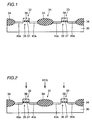
- Step 1 (see Fig. 1): An
element isolation region 31 isolates a firstelement forming region 32 and a secondelement forming region 33 from each other on the main surface of an n-type single-crystalline silicon substrate 30. An elementisolation insulator film 34 is formed on theelement isolation region 31 by a LOCOS (local oxidation of silicon) method. Thereaftergate electrodes 38 consisting of polycrystalline silicon films doped with an impurity are formed on the firstelement forming region 32 and the secondelement forming region 33 throughgate insulator films 37. BF2 is ion-implanted into thesubstrate 30 through thegate electrodes 38 serving as masks, thereby forming low-concentration impurity regions 40a. The conditions for this BF2 ion implantation are injection energy of about 10 keV and a dose of about 5 × 1014 cm-2. - Step 2 (see Fig. 2): A high-temperature short-time
heat treatment is performed by RTA (rapid thermal
annealing) thereby activating the impurity in the low-
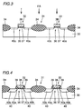
concentration impurity regions 40a and simultaneously recovering from crystal defects (lattice defects) caused in the low-concentration impurity regions 40a by the ion implantation. The conditions for this RTA are a heat source of a halogen lamp, a temperature of about 1000°C to 1200°C, an atmosphere of N2 and a time of about 0.1 sec. to about 30 sec. - Step 3 (see Fig. 3): While the heat treatment by RTA
can be completed in a short time, crystal defects may be
caused in the low-
concentration impurity regions 40a again due to the aforementioned high temperature of at least about 1000°C. Further, it may be impossible to recover from all crystal defects resulting from the ion implantation by the RTA. In the step 3, a heat treatment (FA: furnace anneal) employing an electric furnace is performed thereby recovering from crystal defects resulting from the RTA and remaining crystal defects resulting from the ion implantation left unrecoverable through RTA. More specifically, atoms are recombined and relocated due to the heat treatment employing FA, whereby it is possible to recover from crystal defects resulting from lattice strain of Si. The conditions for this FA are a heat source of an electric furnace, a temperature of about 750°C to about 850°C, an atmosphere of N2 and a time of about 30 min. to about 120 min.The heat treatment by RTA in the aforementioned step 2 corresponds to the "high-temperature heat treatment" or the "first high-temperature heat treatment" in the present invention. The term "high temperature" indicates a temperature capable of recovering from crystal defects resulting from ion implantation and having a possibility of causing new crystal defects. In this embodiment, the "high temperature" means a temperature of at least about 1000°C. The heat treatment by FA in the aforementioned step 3 corresponds to the "low-temperature heat treatment" or the "first low-temperature heat treatment" in the present invention. The term "low temperature" indicates a temperature capable of recovering from crystal defects resulting from RTA (high-temperature heat treatment) and remaining crystal defects resulting from ion implantation, left unrecoverable through RTA, and having no possibility of causing new crystal defects. In this embodiment, the "low temperature" means a temperature of at least 750°C and less than about 1000°C. - Step 4 (see Fig. 4): An insulator film is deposited
to cover the overall surface and thereafter etched back,
thereby forming
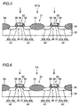
side wall spacers 39 on the side surfaces of thegate electrodes 38. Boron (B) is ion-implanted into thesubstrate 30 through thegate electrodes 38 and theside wall spacers 39 serving as masks, thereby forming high-concentration impurity regions 40b. The conditions for this boron ion implantation are injection energy of about 10 keV and a dose of about 5 × 1015 cm-2. Thus, source/drain regions 40 of an LDD (lightly doped drain) structure consisting of the low-concentration impurity regions 40a and the high-concentration impurity regions 40b are formed. A first field-effect transistor 35 and a second field-effect transistor 36 having thegate insulator films 37, thegate electrodes 38, the source/drain regions 40 and theside wall spacers 39 respectively are formed in the aforementioned manner. - Step 5 (see Fig. 5): A high-temperature short-time
heat treatment employing RTA (rapid thermal annealing) is
performed similarly to the step 2, thereby activating the
impurity in the high-
concentration impurity regions 40b while simultaneously recovering from crystal defects (lattice defects) caused in the high-concentration impurity regions 40b by the ion implantation. The conditions for this RTA are a heat source of a halogen lamp, a temperature of about 1000°C to 1200°C, an atmosphere of N2 and a time of about 0.1 sec. to about 30 sec., similarly to the step 2. - Step 6 (see Fig. 6): A heat treatment (FA: furnace anneal) employing an electric furnace is performed similarly to the step 3, thereby recovering from crystal defects resulting from the RTA and remaining crystal defects resulting from the ion implantation left unrecoverable through the RTA. The conditions for this FA are a heat source of an electric furnace, a temperature of about 750°C to about 850°C, an atmosphere of N2 and a time of about 30 min. to about 120 min., similarly to the step 3. The heat treatment by RTA in the aforementioned step 5 corresponds to the "high-temperature heat treatment" or the "second high-temperature heat treatment" in the present invention. Further, the heat treatment by FA in the aforementioned step 6 corresponds to the "low-temperature heat treatment" or the "second low-temperature heat treatment" in the present invention.
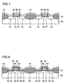
- Step 7 (see Fig. 7): A natural oxide film formed on
the main surface of the
substrate 30 is removed by isotropic etching, and thereafter a titanium (Ti)film 41 is formed on the overall surface of thesubstrate 30 by magnetron sputtering. The thickness of thetitanium film 41 is about 30 nm, for example. Thistitanium film 41 corresponds to the "metal film" in the present invention. - Step 8 (see Fig. 8): A first heat treatment is
performed by a heat treatment employing RTA. As a result
of this heat treatment, titanium silicide (TiSix)
films 42 of a C49 phase are formed in a self-aligned manner on the regions where thetitanium film 41 is in contact with thesubstrate 30 and the regions where thetitanium film 41 is in contact with thegate electrodes 38. Exemplary TiSix is TiSi2. Thesetitanium silicide films 42 correspond to the "compound layer" in the present invention. The conditions for this RTA are a heat source of a halogen lamp, a temperature of about 600°C to about 700°C, an atmosphere of N2 and a time of about 30 sec. The temperature employed for this RTA is less than 1000°C, dissimilarly to the RTA in the step 2.The aforementioned silicification does not occur on the region where thetitanium film 41 is in contact with theelement isolation film 34 and the regions where thetitanium film 41 is in contact with theside wall spacers 39. Therefore, non-silicified portions of thetitanium film 41 remain on the surfaces of these regions. Thin unreacted portions of thetitanium film 41 remain also on the surfaces of thetitanium silicide films 42. - Step 9 (see Fig. 9): The
substrate 30 is dipped in a mixed solution of ammonia, aqueous hydrogen peroxide and water. Thus, the portions of thetitanium film 41 not silicified in the step 8 are removed while leaving only thetitanium silicide films 42. -
- Thereafter a second heat treatment is performed by RTA at a treatment temperature of about 700°C to about 800°C. The remaining conditions for the second heat treatment are identical to those for the first heat treatment. The temperature for this RTA is also less than 1000°C, dissimilarly to the RTA in the step 2. The
titanium silicide films 42 pass into a C54 phase of low resistance from the C49 phase of high resistance due to the second heat treatment. - The first and second field-
effect transistors gate electrodes 38 having thetitanium silicide films 42 on the surfaces and the source/drain regions 40 having thetitanium silicide films 42 on the surfaces is reduced to about 3 Ω/□. - According to this embodiment, as hereinabove described, it is possible to recover from crystal defects resulting from the ion implantation by the RTA, and it is possible to recover from crystal defects resulting from the RTA and remaining crystal defects resulting from the ion implantation, left unrecoverable through the RTA, by the subsequent heat treatment through the electric furnace. Consequently, increase of a leakage current resulting from crystal defects can be effectively prevented.
- Although the present invention has been described and illustrated in detail, it is clearly understood that the same is by way of illustration and example only and is not to be taken by way of limitation, the spirit and scope of the present invention being limited only by the terms of the appended claims.
- For example, the aforementioned embodiment may be modified as follows:
- (1) The field-effect transistors shown in this embodiment have a salicide structure. However, the present invention is not restricted to a semiconductor device having such a salicide structure. The present invention is widely applicable to a method of forming impurity regions by ion implantation and recovering from crystal defects caused in the impurity regions.
- (2) A titanium compound such as titanium nitride may be employed as the metal to be silicified, in place of titanium. Further, a metal having a high melting point other than titanium, such as molybdenum, tungsten, tantalum, hafnium, zirconium, niobium, vanadium, rhenium, chromium, platinum, iridium, osmium, rhodium, cobalt or nickel or a compound thereof may be employed.
- (3) The non-silicified portions of the titanium film may be removed by wet etching. In this case, a mixed solution of aqueous hydrogen peroxide and aqueous ammonia, for example, is employed as the etching solution.
- (4) The present invention may be applied to a method of manufacturing n-channel MOS transistors in place of p-channel MOS transistors.
- (5) A conductive substrate or an insulating substrate of glass or the like may be employed in place of the single-crystalline silicon substrate (semiconductor substrate). While the field-effect transistors are formed on the single-crystalline silicon substrate in the aforementioned embodiment, the present invention is not restricted to this but is also sufficiently applicable to an LCD, for example, having a semiconductor layer formed on an insulating substrate and a device formed on the semiconductor layer. The term "semiconductor substrate" in the present invention indicates a wide concept including not only a general semiconductor substrate but also such a semiconductor layer.
-
Claims (19)
- A method of manufacturing a semiconductor device comprising steps of:forming an impurity region on the main surface of a semiconductor substrate;performing a high-temperature heat treatment for activating said impurity region; andperforming a low-temperature heat treatment after performing said high-temperature heat treatment.
- A method of manufacturing a semiconductor device comprising steps of:forming an impurity region by selectively ion-implanting an impurity into the main surface of a semiconductor substrate;activating said impurity region by performing a high-temperature heat treatment; andrecovering from crystal defects resulting from said high-temperature heat treatment by performing a low-temperature heat treatment after performing said high-temperature heat treatment.
- The method of manufacturing a semiconductor device according to claim 2, further comprising a step of denaturing a surface part of said impurity region to a compound layer with a metal film.
- The method of manufacturing a semiconductor device according to claim 3, whereinsaid step of denaturing said surface part to said compound layer includes a step of forming a metal film on said impurity region and thereafter performing a heat treatment thereby denaturing said surface part of said impurity region to said compound layer with said metal film, andthe temperature for said heat treatment for denaturing said surface part to said compound layer is not in excess of the temperature for said high-temperature heat treatment.
- The method of manufacturing a semiconductor device according to claim 4, whereinsaid heat treatment for denaturing said surface part to said compound layer includes:a first heat treatment for forming said compound layer, anda second heat treatment for reducing the resistance of said formed compound layer, andthe temperature for said first and second heat treatments is not in excess of the temperature for said high-temperature heat treatment.
- The method of manufacturing a semiconductor device according to claim 2, recovering from crystal defects resulting from said ion implantation in addition to activation of said impurity by said high-temperature heat treatment, and
recovering from remaining crystal defects resulting from said ion implantation, left unrecoverable through said high-temperature heat treatment, in addition to recovery from crystal defects resulting from said high-temperature heat treatment by said low-temperature heat treatment. - The method of manufacturing a semiconductor device according to claim 6, whereinthe temperature for said high-temperature heat treatment is at a level capable of recovering from crystal defects resulting from said ion implantation and having a possibility of causing new crystal defects, andthe temperature for said low-temperature heat treatment is at a level capable of recovering from crystal defects resulting from said high-temperature heat treatment and remaining crystal defects resulting from said ion implantation, left unrecoverable through said high-temperature heat treatment, and having no possibility of causing new crystal defects.
- The method of manufacturing a semiconductor device according to claim 7, whereinthe temperature for said high-temperature heat treatment is at least about 1000°C, andthe temperature for said low-temperature heat treatment is at least about 750°C and less than about 1000°C.
- The method of manufacturing a semiconductor device according to claim 2, whereinsaid high-temperature heat treatment is performed for a short time, andsaid low-temperature heat treatment is performed for a long time.
- The method of manufacturing a semiconductor device according to claim 9, whereinsaid high-temperature heat treatment is performed for a time of at least about 0.1 sec. and not more than about 30 sec., andsaid low-temperature heat treatment is performed for a time of at least about 30 min. and not more than about 120 min.
- A method of manufacturing a semiconductor device comprising steps of:forming a low-concentration impurity region by selectively ion-implanting an impurity into the main surface of a semiconductor substrate;activating said low-concentration impurity region by performing a first high-temperature heat treatment;recovering from crystal defects resulting from said first high-temperature heat treatment by performing a first low-temperature heat treatment after performing said first high-temperature heat treatment;forming a high-concentration impurity region by selectively ion-implanting an impurity into the main surface of said semiconductor substrate;activating said high-concentration impurity region by performing a second high-temperature heat treatment; andrecovering from crystal defects resulting from said second high-temperature heat treatment by performing a second low-temperature heat treatment after performing said second high-temperature heat treatment.
- The method of manufacturing a semiconductor device according to claim 11, further comprising a step of denaturing a surface part of said high-concentration impurity region to a compound layer with a metal film.
- The method of manufacturing a semiconductor device according to claim 12, whereinsaid step of denaturing said surface part to said compound layer includes a step of forming a metal film on said high-temperature impurity region and thereafter performing a heat treatment thereby denaturing said surface part of said high-temperature impurity region to said compound layer with said metal film, andthe temperature for said heat treatment for denaturing said surface part to said compound layer is not in excess of the temperature for said first and second high-temperature heat treatments.
- The method of manufacturing a semiconductor device according to claim 13, whereinsaid heat treatment for denaturing said surface part to said compound layer includes:a first heat treatment for forming said compound layer, anda second heat treatment for reducing the resistance of said formed compound layer, andthe temperature for said first and second heat treatments is not in excess of the temperature for said first and second high-temperature heat treatments.
- The method of manufacturing a semiconductor device according to claim 11, recovering from crystal defects resulting from said ion implantation in addition to activation of said impurity by said first and second high-temperature heat treatments, and
recovering from remaining crystal defects resulting from said ion implantation, left unrecoverable through said first and second high-temperature heat treatments, in addition to recovery from said crystal defects resulting from said first and second high-temperature heat treatments by said low-temperature heat treatment. - The method of manufacturing a semiconductor device according to claim 15, whereinthe temperature for said first and second high-temperature heat treatments is at a level capable of recovering from crystal defects resulting from said ion implantation and having a possibility of causing new crystal defects, andthe temperature for said first and second low-temperature heat treatments is at a level capable of recovering from crystal defects resulting from said first and second high-temperature heat treatments and remaining crystal defects resulting from said ion implantation, left unrecoverable through said first and second high-temperature heat treatments, and having no possibility of causing new crystal defects.
- The method of manufacturing a semiconductor device according to claim 16, whereinthe temperature for said first and second high-temperature heat treatments is at least about 1000°C, andthe temperature for said first and second low-temperature heat treatments is at least about 750°C and less than about 1000°C.
- The method of manufacturing a semiconductor device according to claim 11, whereinsaid first and second high-temperature heat treatments are performed for a short time, andsaid first and second low-temperature heat treatments are performed for a long time.
- The method of manufacturing a semiconductor device according to claim 18, whereinsaid first and second high-temperature heat treatments are performed for a time of at least about 0.1 sec. and not more than about 30 sec., andsaid first and second low-temperature heat treatments are performed for a time of at least about 30 min. and not more than about 120 min.
Applications Claiming Priority (4)
| Application Number | Priority Date | Filing Date | Title |
|---|---|---|---|
| JP5873799 | 1999-03-05 | ||
| JP5873799 | 1999-03-05 | ||
| JP2000024448A JP2000323427A (en) | 1999-03-05 | 2000-02-01 | Manufacture of semiconductor device |
| JP2000024448 | 2000-02-01 |
Publications (2)
| Publication Number | Publication Date |
|---|---|
| EP1035565A2 true EP1035565A2 (en) | 2000-09-13 |
| EP1035565A3 EP1035565A3 (en) | 2004-07-07 |
Family
ID=26399759
Family Applications (1)
| Application Number | Title | Priority Date | Filing Date |
|---|---|---|---|
| EP00301383A Withdrawn EP1035565A3 (en) | 1999-03-05 | 2000-02-22 | Method of manufacturing semiconductor device including high-temperature heat treatment |
Country Status (5)
| Country | Link |
|---|---|
| US (1) | US6342440B1 (en) |
| EP (1) | EP1035565A3 (en) |
| JP (1) | JP2000323427A (en) |
| KR (1) | KR20000076772A (en) |
| CN (1) | CN1162896C (en) |
Families Citing this family (6)
| Publication number | Priority date | Publication date | Assignee | Title |
|---|---|---|---|---|
| US6890824B2 (en) * | 2001-08-23 | 2005-05-10 | Matsushita Electric Industrial Co., Ltd. | Semiconductor device and manufacturing method thereof |
| JP2003077854A (en) * | 2001-09-05 | 2003-03-14 | Mitsubishi Electric Corp | Method of manufacturing semiconductor device and semiconductor device |
| JP4594664B2 (en) * | 2004-07-07 | 2010-12-08 | ルネサスエレクトロニクス株式会社 | Manufacturing method of semiconductor device |
| US20060068556A1 (en) * | 2004-09-27 | 2006-03-30 | Matsushita Electric Industrial Co., Ltd. | Semiconductor device and method for fabricating the same |
| JP4795759B2 (en) * | 2005-03-03 | 2011-10-19 | ルネサスエレクトロニクス株式会社 | Method for manufacturing field effect transistor |
| TWI620234B (en) * | 2014-07-08 | 2018-04-01 | 聯華電子股份有限公司 | Method for fabricating semiconductor device |
Citations (6)
| Publication number | Priority date | Publication date | Assignee | Title |
|---|---|---|---|---|
| JPS60119718A (en) * | 1983-12-01 | 1985-06-27 | Nec Corp | Manufacture of semiconductor device |
| JPS63124519A (en) * | 1986-11-14 | 1988-05-28 | Seiko Epson Corp | Manufacture of semiconductor device |
| JPH09293866A (en) * | 1996-02-26 | 1997-11-11 | Sony Corp | Manufacture of semiconductor device |
| US5877050A (en) * | 1996-09-03 | 1999-03-02 | Advanced Micro Devices, Inc. | Method of making N-channel and P-channel devices using two tube anneals and two rapid thermal anneals |
| JPH1187258A (en) * | 1997-09-09 | 1999-03-30 | Toshiba Corp | Manufacture of semiconductor device |
| US5981347A (en) * | 1997-10-14 | 1999-11-09 | Taiwan Semiconductor Manufacturing Company, Ltd. | Multiple thermal annealing method for a metal oxide semiconductor field effect transistor with enhanced hot carrier effect (HCE) resistance |
Family Cites Families (2)
| Publication number | Priority date | Publication date | Assignee | Title |
|---|---|---|---|---|
| US5940699A (en) * | 1996-02-26 | 1999-08-17 | Sony Corporation | Process of fabricating semiconductor device |
| JPH1041407A (en) | 1996-07-19 | 1998-02-13 | Sony Corp | Manufacture of semiconductor device |
-
2000
- 2000-02-01 JP JP2000024448A patent/JP2000323427A/en active Pending
- 2000-02-22 EP EP00301383A patent/EP1035565A3/en not_active Withdrawn
- 2000-03-03 US US09/518,246 patent/US6342440B1/en not_active Expired - Lifetime
- 2000-03-03 CN CNB00103734XA patent/CN1162896C/en not_active Expired - Fee Related
- 2000-03-04 KR KR1020000010889A patent/KR20000076772A/en not_active Application Discontinuation
Patent Citations (6)
| Publication number | Priority date | Publication date | Assignee | Title |
|---|---|---|---|---|
| JPS60119718A (en) * | 1983-12-01 | 1985-06-27 | Nec Corp | Manufacture of semiconductor device |
| JPS63124519A (en) * | 1986-11-14 | 1988-05-28 | Seiko Epson Corp | Manufacture of semiconductor device |
| JPH09293866A (en) * | 1996-02-26 | 1997-11-11 | Sony Corp | Manufacture of semiconductor device |
| US5877050A (en) * | 1996-09-03 | 1999-03-02 | Advanced Micro Devices, Inc. | Method of making N-channel and P-channel devices using two tube anneals and two rapid thermal anneals |
| JPH1187258A (en) * | 1997-09-09 | 1999-03-30 | Toshiba Corp | Manufacture of semiconductor device |
| US5981347A (en) * | 1997-10-14 | 1999-11-09 | Taiwan Semiconductor Manufacturing Company, Ltd. | Multiple thermal annealing method for a metal oxide semiconductor field effect transistor with enhanced hot carrier effect (HCE) resistance |
Non-Patent Citations (5)
| Title |
|---|
| JUANG M H ET AL: "SHALLOW P+N JUNCTIONS FORMED BY USING A TWO-STEP ANNEALING SCHEME WITH LOW THERMAL BUDGET" IEEE ELECTRON DEVICE LETTERS, IEEE INC. NEW YORK, US, vol. 20, no. 12, December 1999 (1999-12), pages 618-620, XP000890736 ISSN: 0741-3106 * |
| PATENT ABSTRACTS OF JAPAN vol. 009, no. 277 (E-355), 6 November 1985 (1985-11-06) & JP 60 119718 A (NIPPON DENKI KK), 27 June 1985 (1985-06-27) * |
| PATENT ABSTRACTS OF JAPAN vol. 012, no. 375 (E-666), 7 October 1988 (1988-10-07) & JP 63 124519 A (SEIKO EPSON CORP), 28 May 1988 (1988-05-28) * |
| PATENT ABSTRACTS OF JAPAN vol. 1998, no. 03, 27 February 1998 (1998-02-27) & JP 09 293866 A (SONY CORP), 11 November 1997 (1997-11-11) & US 5 940 699 A 17 August 1999 (1999-08-17) * |
| PATENT ABSTRACTS OF JAPAN vol. 1999, no. 08, 30 June 1999 (1999-06-30) & JP 11 087258 A (TOSHIBA CORP), 30 March 1999 (1999-03-30) * |
Also Published As
| Publication number | Publication date |
|---|---|
| JP2000323427A (en) | 2000-11-24 |
| US6342440B1 (en) | 2002-01-29 |
| CN1162896C (en) | 2004-08-18 |
| CN1266280A (en) | 2000-09-13 |
| KR20000076772A (en) | 2000-12-26 |
| EP1035565A3 (en) | 2004-07-07 |
Similar Documents
| Publication | Publication Date | Title |
|---|---|---|
| US6436747B1 (en) | Method of fabricating semiconductor device | |
| JP2891092B2 (en) | Method for manufacturing semiconductor device | |
| KR101055708B1 (en) | How to Form Dual Salicide in CMOS Technology | |
| US7396767B2 (en) | Semiconductor structure including silicide regions and method of making same | |
| US6248637B1 (en) | Process for manufacturing MOS Transistors having elevated source and drain regions | |
| JP3348070B2 (en) | Method for manufacturing semiconductor device | |
| US6737710B2 (en) | Transistor structure having silicide source/drain extensions | |
| JPH11111980A (en) | Semiconductor device and its manufacture | |
| US6451679B1 (en) | Ion mixing between two-step titanium deposition process for titanium salicide CMOS technology | |
| KR0183490B1 (en) | Fabrication process for semiconductor device having mos type field effect transistor | |
| US6518631B1 (en) | Multi-Thickness silicide device formed by succesive spacers | |
| KR100722936B1 (en) | Metal oxide semiconductor field effect transistor and method for forming the same | |
| JPH11284179A (en) | Semiconductor device and manufacture thereof | |
| US6342440B1 (en) | Method for forming low-leakage impurity regions by sequence of high-and low-temperature treatments | |
| JPH11186545A (en) | Manufacture of semiconductor device having silicide and ldd structure | |
| JP3295931B2 (en) | Method for manufacturing semiconductor device | |
| JPH09199720A (en) | Mos type semiconductor device and its fabrication | |
| JPH10313117A (en) | Mis transistor and manufacture thereof | |
| US7211489B1 (en) | Localized halo implant region formed using tilt pre-amorphization implant and laser thermal anneal | |
| JP3581253B2 (en) | Semiconductor device and manufacturing method thereof | |
| JPH11214328A (en) | Semiconductor device and manufacturing method | |
| JPH06216324A (en) | Manufacture of semiconductor device | |
| JPH0831949A (en) | Dual gate structure cmos semiconductor device and its manufacture | |
| JPH11177103A (en) | Semiconductor device | |
| KR100276876B1 (en) | How to compensate silicide lost after contact etching |
Legal Events
| Date | Code | Title | Description |
|---|---|---|---|
| PUAI | Public reference made under article 153(3) epc to a published international application that has entered the european phase |
Free format text: ORIGINAL CODE: 0009012 |
|
| 17P | Request for examination filed |
Effective date: 20000313 |
|
| AK | Designated contracting states |
Kind code of ref document: A2 Designated state(s): AT BE CH CY DE DK ES FI FR GB GR IE IT LI LU MC NL PT SE |
|
| AX | Request for extension of the european patent |
Free format text: AL;LT;LV;MK;RO;SI |
|
| RIC1 | Information provided on ipc code assigned before grant |
Ipc: 7H 01L 21/324 B Ipc: 7H 01L 21/8238 B Ipc: 7H 01L 21/336 B Ipc: 7H 01L 21/265 A |
|
| PUAL | Search report despatched |
Free format text: ORIGINAL CODE: 0009013 |
|
| AK | Designated contracting states |
Kind code of ref document: A3 Designated state(s): AT BE CH CY DE DK ES FI FR GB GR IE IT LI LU MC NL PT SE |
|
| AX | Request for extension of the european patent |
Extension state: AL LT LV MK RO SI |
|
| 17Q | First examination report despatched |
Effective date: 20050111 |
|
| AKX | Designation fees paid |
Designated state(s): DE FR GB IT NL |
|
| STAA | Information on the status of an ep patent application or granted ep patent |
Free format text: STATUS: THE APPLICATION IS DEEMED TO BE WITHDRAWN |
|
| 18D | Application deemed to be withdrawn |
Effective date: 20050522 |