EP1033749A2 - Method and producing ceramic multilayer substrate - Google Patents
Method and producing ceramic multilayer substrate Download PDFInfo
- Publication number
- EP1033749A2 EP1033749A2 EP00104260A EP00104260A EP1033749A2 EP 1033749 A2 EP1033749 A2 EP 1033749A2 EP 00104260 A EP00104260 A EP 00104260A EP 00104260 A EP00104260 A EP 00104260A EP 1033749 A2 EP1033749 A2 EP 1033749A2
- Authority
- EP
- European Patent Office
- Prior art keywords
- glass
- ceramic green
- inorganic composition
- green sheets
- ceramic
- Prior art date
- Legal status (The legal status is an assumption and is not a legal conclusion. Google has not performed a legal analysis and makes no representation as to the accuracy of the status listed.)
- Granted
Links
Images



Classifications
-
- H—ELECTRICITY
- H05—ELECTRIC TECHNIQUES NOT OTHERWISE PROVIDED FOR
- H05K—PRINTED CIRCUITS; CASINGS OR CONSTRUCTIONAL DETAILS OF ELECTRIC APPARATUS; MANUFACTURE OF ASSEMBLAGES OF ELECTRICAL COMPONENTS
- H05K3/00—Apparatus or processes for manufacturing printed circuits
- H05K3/46—Manufacturing multilayer circuits
- H05K3/4611—Manufacturing multilayer circuits by laminating two or more circuit boards
- H05K3/4626—Manufacturing multilayer circuits by laminating two or more circuit boards characterised by the insulating layers or materials
- H05K3/4629—Manufacturing multilayer circuits by laminating two or more circuit boards characterised by the insulating layers or materials laminating inorganic sheets comprising printed circuits, e.g. green ceramic sheets
-
- H—ELECTRICITY
- H10—SEMICONDUCTOR DEVICES; ELECTRIC SOLID-STATE DEVICES NOT OTHERWISE PROVIDED FOR
- H10W—GENERIC PACKAGES, INTERCONNECTIONS, CONNECTORS OR OTHER CONSTRUCTIONAL DETAILS OF DEVICES COVERED BY CLASS H10
- H10W70/00—Package substrates; Interposers; Redistribution layers [RDL]
- H10W70/01—Manufacture or treatment
- H10W70/05—Manufacture or treatment of insulating or insulated package substrates, or of interposers, or of redistribution layers
-
- H—ELECTRICITY
- H10—SEMICONDUCTOR DEVICES; ELECTRIC SOLID-STATE DEVICES NOT OTHERWISE PROVIDED FOR
- H10W—GENERIC PACKAGES, INTERCONNECTIONS, CONNECTORS OR OTHER CONSTRUCTIONAL DETAILS OF DEVICES COVERED BY CLASS H10
- H10W70/00—Package substrates; Interposers; Redistribution layers [RDL]
- H10W70/60—Insulating or insulated package substrates; Interposers; Redistribution layers
- H10W70/67—Insulating or insulated package substrates; Interposers; Redistribution layers characterised by their insulating layers or insulating parts
- H10W70/68—Shapes or dispositions thereof
- H10W70/685—Shapes or dispositions thereof comprising multiple insulating layers
-
- H—ELECTRICITY
- H05—ELECTRIC TECHNIQUES NOT OTHERWISE PROVIDED FOR
- H05K—PRINTED CIRCUITS; CASINGS OR CONSTRUCTIONAL DETAILS OF ELECTRIC APPARATUS; MANUFACTURE OF ASSEMBLAGES OF ELECTRICAL COMPONENTS
- H05K1/00—Printed circuits
- H05K1/02—Details
- H05K1/03—Use of materials for the substrate
- H05K1/0306—Inorganic insulating substrates, e.g. ceramic, glass
-
- H—ELECTRICITY
- H05—ELECTRIC TECHNIQUES NOT OTHERWISE PROVIDED FOR
- H05K—PRINTED CIRCUITS; CASINGS OR CONSTRUCTIONAL DETAILS OF ELECTRIC APPARATUS; MANUFACTURE OF ASSEMBLAGES OF ELECTRICAL COMPONENTS
- H05K2201/00—Indexing scheme relating to printed circuits covered by H05K1/00
- H05K2201/01—Dielectrics
- H05K2201/0183—Dielectric layers
- H05K2201/0195—Dielectric or adhesive layers comprising a plurality of layers, e.g. in a multilayer structure
-
- H—ELECTRICITY
- H10—SEMICONDUCTOR DEVICES; ELECTRIC SOLID-STATE DEVICES NOT OTHERWISE PROVIDED FOR
- H10W—GENERIC PACKAGES, INTERCONNECTIONS, CONNECTORS OR OTHER CONSTRUCTIONAL DETAILS OF DEVICES COVERED BY CLASS H10
- H10W70/00—Package substrates; Interposers; Redistribution layers [RDL]
- H10W70/60—Insulating or insulated package substrates; Interposers; Redistribution layers
- H10W70/67—Insulating or insulated package substrates; Interposers; Redistribution layers characterised by their insulating layers or insulating parts
- H10W70/68—Shapes or dispositions thereof
- H10W70/682—Shapes or dispositions thereof comprising holes having chips therein
-
- H—ELECTRICITY
- H10—SEMICONDUCTOR DEVICES; ELECTRIC SOLID-STATE DEVICES NOT OTHERWISE PROVIDED FOR
- H10W—GENERIC PACKAGES, INTERCONNECTIONS, CONNECTORS OR OTHER CONSTRUCTIONAL DETAILS OF DEVICES COVERED BY CLASS H10
- H10W72/00—Interconnections or connectors in packages
- H10W72/071—Connecting or disconnecting
- H10W72/072—Connecting or disconnecting of bump connectors
- H10W72/07251—Connecting or disconnecting of bump connectors characterised by changes in properties of the bump connectors during connecting
-
- H—ELECTRICITY
- H10—SEMICONDUCTOR DEVICES; ELECTRIC SOLID-STATE DEVICES NOT OTHERWISE PROVIDED FOR
- H10W—GENERIC PACKAGES, INTERCONNECTIONS, CONNECTORS OR OTHER CONSTRUCTIONAL DETAILS OF DEVICES COVERED BY CLASS H10
- H10W72/00—Interconnections or connectors in packages
- H10W72/20—Bump connectors, e.g. solder bumps or copper pillars; Dummy bumps; Thermal bumps
-
- H—ELECTRICITY
- H10—SEMICONDUCTOR DEVICES; ELECTRIC SOLID-STATE DEVICES NOT OTHERWISE PROVIDED FOR
- H10W—GENERIC PACKAGES, INTERCONNECTIONS, CONNECTORS OR OTHER CONSTRUCTIONAL DETAILS OF DEVICES COVERED BY CLASS H10
- H10W90/00—Package configurations
- H10W90/701—Package configurations characterised by the relative positions of pads or connectors relative to package parts
- H10W90/721—Package configurations characterised by the relative positions of pads or connectors relative to package parts of bump connectors
- H10W90/724—Package configurations characterised by the relative positions of pads or connectors relative to package parts of bump connectors between a chip and a stacked insulating package substrate, interposer or RDL
-
- Y—GENERAL TAGGING OF NEW TECHNOLOGICAL DEVELOPMENTS; GENERAL TAGGING OF CROSS-SECTIONAL TECHNOLOGIES SPANNING OVER SEVERAL SECTIONS OF THE IPC; TECHNICAL SUBJECTS COVERED BY FORMER USPC CROSS-REFERENCE ART COLLECTIONS [XRACs] AND DIGESTS
- Y10—TECHNICAL SUBJECTS COVERED BY FORMER USPC
- Y10T—TECHNICAL SUBJECTS COVERED BY FORMER US CLASSIFICATION
- Y10T156/00—Adhesive bonding and miscellaneous chemical manufacture
- Y10T156/10—Methods of surface bonding and/or assembly therefor
- Y10T156/1052—Methods of surface bonding and/or assembly therefor with cutting, punching, tearing or severing
- Y10T156/1056—Perforating lamina
-
- Y—GENERAL TAGGING OF NEW TECHNOLOGICAL DEVELOPMENTS; GENERAL TAGGING OF CROSS-SECTIONAL TECHNOLOGIES SPANNING OVER SEVERAL SECTIONS OF THE IPC; TECHNICAL SUBJECTS COVERED BY FORMER USPC CROSS-REFERENCE ART COLLECTIONS [XRACs] AND DIGESTS
- Y10—TECHNICAL SUBJECTS COVERED BY FORMER USPC
- Y10T—TECHNICAL SUBJECTS COVERED BY FORMER US CLASSIFICATION
- Y10T29/00—Metal working
- Y10T29/49—Method of mechanical manufacture
- Y10T29/49002—Electrical device making
- Y10T29/49117—Conductor or circuit manufacturing
- Y10T29/49124—On flat or curved insulated base, e.g., printed circuit, etc.
- Y10T29/49155—Manufacturing circuit on or in base
- Y10T29/49163—Manufacturing circuit on or in base with sintering of base
-
- Y—GENERAL TAGGING OF NEW TECHNOLOGICAL DEVELOPMENTS; GENERAL TAGGING OF CROSS-SECTIONAL TECHNOLOGIES SPANNING OVER SEVERAL SECTIONS OF THE IPC; TECHNICAL SUBJECTS COVERED BY FORMER USPC CROSS-REFERENCE ART COLLECTIONS [XRACs] AND DIGESTS
- Y10—TECHNICAL SUBJECTS COVERED BY FORMER USPC
- Y10T—TECHNICAL SUBJECTS COVERED BY FORMER US CLASSIFICATION
- Y10T428/00—Stock material or miscellaneous articles
- Y10T428/24—Structurally defined web or sheet [e.g., overall dimension, etc.]
- Y10T428/24802—Discontinuous or differential coating, impregnation or bond [e.g., artwork, printing, retouched photograph, etc.]
- Y10T428/24917—Discontinuous or differential coating, impregnation or bond [e.g., artwork, printing, retouched photograph, etc.] including metal layer
-
- Y—GENERAL TAGGING OF NEW TECHNOLOGICAL DEVELOPMENTS; GENERAL TAGGING OF CROSS-SECTIONAL TECHNOLOGIES SPANNING OVER SEVERAL SECTIONS OF THE IPC; TECHNICAL SUBJECTS COVERED BY FORMER USPC CROSS-REFERENCE ART COLLECTIONS [XRACs] AND DIGESTS
- Y10—TECHNICAL SUBJECTS COVERED BY FORMER USPC
- Y10T—TECHNICAL SUBJECTS COVERED BY FORMER US CLASSIFICATION
- Y10T428/00—Stock material or miscellaneous articles
- Y10T428/24—Structurally defined web or sheet [e.g., overall dimension, etc.]
- Y10T428/24802—Discontinuous or differential coating, impregnation or bond [e.g., artwork, printing, retouched photograph, etc.]
- Y10T428/24926—Discontinuous or differential coating, impregnation or bond [e.g., artwork, printing, retouched photograph, etc.] including ceramic, glass, porcelain or quartz layer
-
- Y—GENERAL TAGGING OF NEW TECHNOLOGICAL DEVELOPMENTS; GENERAL TAGGING OF CROSS-SECTIONAL TECHNOLOGIES SPANNING OVER SEVERAL SECTIONS OF THE IPC; TECHNICAL SUBJECTS COVERED BY FORMER USPC CROSS-REFERENCE ART COLLECTIONS [XRACs] AND DIGESTS
- Y10—TECHNICAL SUBJECTS COVERED BY FORMER USPC
- Y10T—TECHNICAL SUBJECTS COVERED BY FORMER US CLASSIFICATION
- Y10T428/00—Stock material or miscellaneous articles
- Y10T428/24—Structurally defined web or sheet [e.g., overall dimension, etc.]
- Y10T428/24942—Structurally defined web or sheet [e.g., overall dimension, etc.] including components having same physical characteristic in differing degree
-
- Y—GENERAL TAGGING OF NEW TECHNOLOGICAL DEVELOPMENTS; GENERAL TAGGING OF CROSS-SECTIONAL TECHNOLOGIES SPANNING OVER SEVERAL SECTIONS OF THE IPC; TECHNICAL SUBJECTS COVERED BY FORMER USPC CROSS-REFERENCE ART COLLECTIONS [XRACs] AND DIGESTS
- Y10—TECHNICAL SUBJECTS COVERED BY FORMER USPC
- Y10T—TECHNICAL SUBJECTS COVERED BY FORMER US CLASSIFICATION
- Y10T428/00—Stock material or miscellaneous articles
- Y10T428/24—Structurally defined web or sheet [e.g., overall dimension, etc.]
- Y10T428/24942—Structurally defined web or sheet [e.g., overall dimension, etc.] including components having same physical characteristic in differing degree
- Y10T428/2495—Thickness [relative or absolute]
-
- Y—GENERAL TAGGING OF NEW TECHNOLOGICAL DEVELOPMENTS; GENERAL TAGGING OF CROSS-SECTIONAL TECHNOLOGIES SPANNING OVER SEVERAL SECTIONS OF THE IPC; TECHNICAL SUBJECTS COVERED BY FORMER USPC CROSS-REFERENCE ART COLLECTIONS [XRACs] AND DIGESTS
- Y10—TECHNICAL SUBJECTS COVERED BY FORMER USPC
- Y10T—TECHNICAL SUBJECTS COVERED BY FORMER US CLASSIFICATION
- Y10T428/00—Stock material or miscellaneous articles
- Y10T428/24—Structurally defined web or sheet [e.g., overall dimension, etc.]
- Y10T428/24942—Structurally defined web or sheet [e.g., overall dimension, etc.] including components having same physical characteristic in differing degree
- Y10T428/2495—Thickness [relative or absolute]
- Y10T428/24959—Thickness [relative or absolute] of adhesive layers
Definitions
- the present invention relates to a method of producing a ceramic multilayer substrate on which semiconductor LSI, a chip components, or the like are mounted and wired to each other.
- Japanese Unexamined Patent Publication No. 5-102666 discloses a conventional method of producing a ceramic multilayer substrate.
- plural glass-ceramic green sheets made of a glass-ceramic, containing an organic binder and a plasticizer, and having a conductor pattern (not illustrated) formed on the surfaces thereof by use of a conductor paste composition are first laminated to form a laminate 101.
- ceramic green sheets 102 and 103 containing as a major component an inorganic composition having a sintering temperature higher than that of the glass-ceramic green sheet 101 are formed on the back and front sides of the laminate 101, respectively, and thereafter, pressure-bonded together to form a lamination pressure-bonding body 100.
- the lamination pressure-bonding body 100 is fired under the firing conditions for the laminate 101. Thereafter, the unsintered ceramic green sheets 102 and 103 are removed, whereby a ceramic multilayer substrate is obtained.
- the laminate 101 is inhibited from heat shrinking in the plane direction at firing, owing to the ceramic green sheets 102 and 103 of the lamination pressure-bonding body 100.
- Such a conventional method of producing a ceramic multilayer substrate has the following problems.
- the vicinities of the ceramic green sheets 102 and 103 that is, the vicinities of the front and back sides of the laminate 101 are inhibited from heat shrinking in the plane direction.
- the central portion 104 in the thickness direction of the laminate 101 is distorted so as to be depressed toward the inside thereof as shown in FIG. 2.
- distortion 104' causes the inside of the laminate 101 to because cracked and the glass-ceramic green sheets to peel away from each other.
- preferred embodiments of the present invention provides a method of producing a ceramic multilayer substrate in which the side faces of the laminate can be prevented from being distorted so as to be depressed toward the inside thereof, caused by the heat shrinkage at firing.
- One preferred embodiment of the present invention provides a method of producing a ceramic multilayer substrate by lamination of plural glass-ceramic green sheets made of a glass-ceramic containing an organic binder and a plasticizer to form a laminate, and firing of the laminate comprises the step of applying to or overlaying on the surfaces of the glass-ceramic green sheets inorganic compositions having a higher sintering temperature than the glass-ceramic green sheets, the step of laminating a plurality of the glass-ceramic green sheets having the inorganic compositions applied to or overlaid on the surfaces of the glass-ceramic green sheets to form a part of the laminate, and the step of laminating a plurality of the glass-ceramic green sheets to form the other part of the laminate.
- the above described method may include the step of forming one of the glass-ceramic green sheets so as to have a smaller thickness than each of the other glass-ceramic green sheets, the step of applying to or overlaying on the surface of the glass-ceramic green sheet having a smaller thickness the inorganic composition, the step of arranging the glass-ceramic green sheet having a smaller thickness as the undermost layer of the laminate, and the step of laminating a plurality of the glass-ceramic green sheets having the inorganic compositions applied to or overlaid on the surfaces thereof, whereby a part of or the whole of the laminate ranging from the vicinity of the undermost layer to the uppermost layer is formed.
- the above described method may include the step of laminating a plurality of the glass-ceramic green sheets having the inorganic compositions provided on the surfaces thereof, whereby a part of or the whole of the laminate ranging from the undermost layer to the vicinity of the uppermost layer is formed, and the step of laminating the glass-ceramic green sheet as the uppermost layer of the laminate.
- the method may include the step of forming the glass-ceramic green sheets to constitute the undermost and uppermost layers of the laminate so as to have a smaller thickness than the respective glass-ceramic green sheets to constitute the other layers of the laminate.
- the method may include the step of forming opening portions through a plurality of the glass-ceramic green sheets arranged as the uppermost layer of the laminate and in its vicinities and also the inorganic compositions applied to or overlaid on the glass-ceramic green sheets, and the step of laminating a plurality of the glass-ceramic green sheets having the opening portions formed therein to form the laminate having a cavity formed of the opening portions of the plural glass-ceramic green sheets which are made continuous to each other.
- the inorganic compositions applied to or overlaid on the glass-ceramic green sheets may contain alumina as a major component.
- each of the inorganic compositions applied to or overlaid on the glass-ceramic green sheets may have a thickness of from about 1 to 20 ⁇ m.
- the differences between the sintering temperatures of the glass-ceramic green sheets and the sintering temperatures of the inorganic compositions applied to or overlaid on the glass-ceramic green sheets is at least about 100°C.
- the above described method may include the step of forming a glass-ceramic green sheet on a carrier film, and then applying to or overlaying on the glass-ceramic green sheet the inorganic composition to form an inorganic composition layer, the step of forming a perforation through each of the carrier film, the glass-ceramic green sheet and the inorganic composition layer, filling a conductor material into the perforation to produce a viahole, and further forming a conductor pattern on the inorganic composition layer, and the step of releasing the glass-ceramic green sheet having the viahole and the conductor pattern, together with the inorganic composition layer, from the carrier film and laminating the glass-ceramic green sheets with the inorganic composition layers, sequentially.
- the method may include the step of applying to or overlaying on a carrier film the inorganic composition to form an inorganic composition layer, and then forming a glass-ceramic green sheet on the inorganic composition layer, the step of forming a perforation through each of the carrier film, the inorganic composition layer and the glass-ceramic green sheet, then filling a conductor material into the perforation to form a viahole, and forming a conductor pattern on the glass-ceramic green sheet, and the step of releasing the glass-ceramic green sheet having the viahole and the conductor pattern, together with the inorganic composition layer, from the carrier film and laminating the glass-ceramic green sheets with the inorganic composition layers sequentially.
- a glass-ceramic green sheet having a viahole and a conductor pattern and a green sheet having a perforation not filled with a conductor material, corresponding to the viahole and containing the inorganic composition as a major component may be laminated to form a part of the laminate.
- the glass-ceramic green sheets and the inorganic compositions having a higher sintering temperature than the respective glass-ceramic green sheets are alternately arranged to form a laminate, and fired.
- the glass-ceramic green sheets constituting not only the undermost and uppermost layers of the laminate but also the internal layers are inhibited from heat shrinking in the plane direction. Accordingly, there is little danger that distortion of the laminate occurs at firing, that is, the side faces of the laminate are distorted so as to be depressed toward the inside. Therefore, the generation of cracks and the peeling of the glass-ceramic green sheets are prevented.
- the production of a high precision ceramic multilayer substrate is enabled.
- the sintered glass-ceramics after the laminate is fired can be used as the mounting surfaces of the ceramic multilayer substrate. Accordingly, the mounting surfaces are stable, and the ceramic multilayer substrate can be mounted without fail as compared with the surfaces made of unsintered inorganic compositions.
- the glass-ceramic green sheets constituting the undermost or uppermost layer of the laminate or both of them so as to have a smaller thickness than the respective glass-ceramic green sheets constituting the other layers of the laminate, the amount of change caused by heat shrinkage of the respective layers can be made equal to each other. Accordingly, the peeling or the generation of cracks can be prevented from occurring between the glass-ceramic green sheets.
- the inorganic composition having a higher sintering temperature than the glass-ceramic green sheet is exposed on the bottom of the cavity formed in the laminate. Accordingly, it is unnecessary to provide an inorganic composition on the bottom of the cavity after the cavity is formed.
- the bottom of the cavity can be simply protected from heat shrinking at firing.
- the unsintered inorganic compositions function as a buffering material against vibration, impact and thermal shock. Accordingly, cracks or breaks fatal to the laminate are not generated.
- the glass-ceramic green sheets constituting the laminate and the inorganic compositions for inhibiting the heat shrinkage at firing have different sintering temperatures, the co-firing of the whole laminate is possible, and the simplification of the manufacturing process and the reduction of the manufacturing cost can be realized.
- the materials for use in the inorganic composition to inhibit the heat shrinkage include no glass, even though the conductor constituting the internal electrodes is diffused was firing of the laminate, caused by the plastic flow of the glass-ceramic green sheets, diffusion can be inhibited owing to the inorganic compositions for inhibiting the heat shrinkage.
- a method of producing a ceramic multilayer substrate according to a first embodiment of the present invention is described by use of the drawings.
- a paste (slurry) made of an inorganic oxide composition containing alumina as a major component is applied to the surfaces of the respective glass-ceramic green sheets constituting a laminate.
- this will be described in the order of formation.
- a glass-ceramic green sheet is formed as follows.
- a glass-ceramic which consists of a composition comprising lead borosilicate glass powder and alumina powder at a ratio by weight of 50 : 50 is added to an organic binder comprising polyvinylbutyral, a plasticizer comprising di-n-butylphthalate, and a solvent produced by mixing toluene and isopropyl alcohol at a ratio by weight of 30 : 70, and mixed to form slurry.
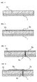
- the slurry is sheet-formed on a carrier film 1 by the doctor-blade method as shown in FIG. 3, and dried to form a glass-ceramic green sheet 2c.
- an inorganic composition layer 3c is formed on the glass-ceramic green sheet 2c which is formed on the carrier film 1.
- the inorganic composition layer 3c is formed by applying a paste (slurry) to the surface of the glass-ceramic green sheet 2c and drying, the paste being produced by adding alumina powder to an organic binder comprising polyvinylbutyral, a plasticizer comprising di-n-butylphthalate, and a solvent produced by mixing toluene and isopropyl alcohol at a ratio by weight of 30 : 70, and mixing them.
- the alumina has a higher sintering temperature than the glass-ceramic green sheet 2c.
- the inorganic composition layer 3c containing the alumina as a major component has a higher sintering temperature than the glass-ceramic green sheet 2c. That is, the inorganic composition layer 3c can not be sintered under the sintering conditions for the glass-ceramic green sheet 2c.
- Zirconium oxide, aluminum nitride, boron nitride, mullite, magnesium oxide, silicon carbide, or the like, may be substituted for alumina used as a material for the inorganic composition layer 3c.
- a conductor material (conductor paste) is filled by screen printing or the like, whereby a viahole 4c is formed through the carrier film 1, the glass-ceramic green sheet 2c and the inorganic composition layer 3c, as shown in FIG. 5.
- a vehicle comprising ethyl cellulose as an organic binder dissolved in terpineol is added to an inorganic component comprising 5 weight parts of glass frit and 100 weight parts of silver powder. Powders of copper, silver/palladium or silver/platinum or the like may be substituted for the silver powder used as an inorganic component of the conductor paste.
- a conductor paste is printed on the inorganic composition layer 3c formed on the glass-ceramic green sheet 2c by a screen printing method, whereby a conductor pattern 5c connecting to the viaholes 4c is formed.
- the conductor pattern 5c may also be formed by use of metal foil or a metallic wire.
- metal foil or a metallic wire available are a method of hot pressing a punched metal foil or metal wire against a ceramic green sheet, or a method of forming a pattern on a resin film by vapor deposition, sputtering, plating or the like, and heat transferring the pattern onto a ceramic green sheet.
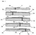
- a plurality of the glass-ceramic green sheets 2c formed by the procedures (1) through (4) are peeled from the carrier films 1, respectively.
- the glass-ceramic green sheets 2c, together with the glass-ceramic green sheets 2a, 2b, 2d prepared by a technique similar to the above-described one, are sequentially laminated, with the surface sides thereof where the inorganic composition layer 3c and the conductor pattern 5c are formed, being on the upper sides thereof.
- the inorganic composition layers 3b and 3d are formed on one of the main sides thereof, similarly to the glass-ceramic green sheet 2c, viaholes 4b and 4d are formed so as to perforate through the glass-ceramic green sheets 2b and 2d, and the inorganic composition layers 3b and 3d, and conductor patterns 5b and 5d are formed on the surfaces of the surfaces of the inorganic composition layers 3b and 3d, respectively.
- the glass-ceramic green sheet 2a constituting the undermost layer of the ceramic multilayer substrate, and the glass-ceramic green sheet 2e constituting the uppermost layer of the ceramic multilayer substrate each have a thickness which is smaller than the glass-ceramic green sheets 2b, 2c, 2d or the like constituting the other layers. Further, as to the glass-ceramic green sheet 2a, after the carder film is released, a conductor pattern 8 to function as a surface electrode is also formed on the back side thereof where the inorganic composition layer 3a is not provided and a conductor patterns 5a is formed on the front side and the two conductors are interconnected by viahole 4a.
- the conductor pattern 8 to function as a surface electrode may also be formed by printing the conductor pattern and baking after the ceramic multilayer substrate is fired.
- the glass-ceramic green sheet 2e constituting the uppermost layer of the ceramic multilayer substrate with a conductor pattern 7 and viahole 4e are formed in compliance with the procedures for producing ordinary glass-ceramic green sheets without the inorganic composition layer being formed thereon.
- the glass-ceramic green sheets 2a through 2e are hot pressure-bonding under the conditions of a temperature of 80°C and a pressure of 200 kg/cm 2 , for example, to form a lamination pressure-bonded body.
- the glass-ceramic green sheets 2a through 2e are bonded to the inorganic composition layers 3a through 3d, owing to the anchor effects and so forth.
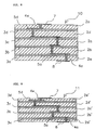
- FIG. 8 shows the lamination pressure-bonded body formed as described above.
- reference numeral 10 designates the lamination pressure-bonded body, in which the glass-ceramic green sheets 2a through 2e and the inorganic composition layers 3a through 3d are alternately arranged, and the conductor patterns 7 and 8 formed on the front and back sides thereof to function as surface electrodes and the conductor patterns 5a through 5d provided between the respective layers to function as internal electrodes are connected to each other through viaholes 4a through 4e.
- each of the glass-ceramic green sheets 2b through 2d constituting the lamination pressure-bonded body 10 the opposite sides thereof are coated with the inorganic composition layers 3a through 3d.
- the glass-ceramic green sheet 2a constituting the undermost layer of the lamination pressure-bonded body 10, and the glass-ceramic green sheet 2e constituting the uppermost layer have a smaller thickness than the glass-ceramic green sheets 2b through 2d of the other layers.
- the lamination pressure-bonded body 10 is fired in the air or in the nitrogen atmosphere under the conditions of a temperature of 900°C and 1 hour, for example.
- the glass-ceramic green sheets constituting the lamination pressure-bonded body 10 are allowed to heat-shrink in the x, y, and z directions.
- the glass-ceramic green sheets are "restrained" by the inorganic composition layers 3a through 3d, which are arranged alternately with the glass-ceramic green sheets. Accordingly, as shown in FIG. 9, the heat shrinkage in the plane direction (x - y direction) is restrained, and the green sheets considerably shrunk only in the thickness direction (2 direction). That is, the glass-ceramic green sheets 2a through 2e as shown in FIG. 8 considerably shrink in the thickness direction to become the glass-ceramic bodies 2a' through 2e' in the sintered body (ceramic multilayer substrate) 11 as shown in FIG. 9.
- the restraint is brought about as follows.
- the glass components of the glass-ceramic green sheets 2a through 2e are diffused and permeated into the inorganic composition layers 3a through 3d at firing.
- the glass-ceramic green sheets 2a through 2e are strongly bonded to the inorganic composition layers 3a through 3d before the glass-ceramic green sheets 2a through 2e substantially start to shrink.
- the sintering of the inorganic composition layers 3a through 3d does not proceed.
- the lamination pressure-bonded body 10 is distorted at firing, especially the side faces thereof being distorted so as to be depressed toward the inside thereof. Accordingly, the generation of cracks and the peeling of the glass-ceramic green sheets 2a through 2e are prevented.
- the production of a high precision ceramic multilayer substrate 11 can be produced.
- the heat shrinkage restraining degrees of the respective glass-ceramic green sheets 2a and 2e are small compared with the glass-ceramic green sheets 2b, 2c and 2d since for each of the glass-ceramic green sheets 2a and 2e, only one of the main faces thereof is contacted with the inorganic composition layer. However, since the thicknesses of the glass-ceramic green sheets 2a and 2e are smaller than those of the glass-ceramic green sheets 2b, 2c and 2d, respectively, the amount of change caused by the heat shrinkage are small.
- each thickness of the respective glass-ceramic green sheets of the uppermost and undermost layers is about 0.1 - 0.9 times, preferably about 0.3 - 0.7 times, that of the other glass-ceramic green sheets.
- the amount of change caused by heat shrinkage in the method of producing a ceramic multilayer substrate according to the first embodiment of the present invention between the glass-ceramic green sheets 2a and 2b, between the glass-ceramic green sheets 2b and 2c, between the glass-ceramic green sheets 2c and 2d, and between the glass-ceramic green sheets 2d and 2e are essentially equal to each other. Accordingly, a high precision ceramic multilayer substrate can be attained in which peeling between the respective glass-ceramic green sheets and the generation of cracks are prevented, and moreover warp and distortion are reduced.
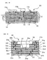
- the ceramic multilayer substrate 11 as shown in FIG. 9 can be used as a substrate for a ceramic multilayer module 20 as shown in FIG.10, for example.
- the ceramic multilayer module 20 contains a coil pattern, a capacitor pattern or the like, which is formed by internal electrodes 15, viaholes 14, or the like, and includes a substrate produced by alternately laminating glass-ceramic green sheets 12 and inorganic composition layers 13.
- semiconductor devices 19a and 19b, a chip monolithic capacitor 19c, and so forth are mounted on one of the main sides.
- Land electrodes 18 are formed on the other main side.
- the thicknesses of the glass-ceramic green sheets of the uppermost and undermost layers may be substantially equal to those of the other glass-ceramic green sheets in the ceramic multilayer module 20. However, preferably, the thicknesses of the glass-ceramic green sheets as the uppermost and undermost layers are smaller than those of the other glass-ceramic green sheets, similarly to the above-described ceramic multilayer substrate 11.
- Opening portions are formed in glass-ceramic green sheets 31e through 31h constituting the uppermost layer of the laminate and its vicinities so as to perforate through the glass-ceramic green sheets and the inorganic composition layers applied to or overlaid on the glass-ceramic green sheets by use of a perforator.
- the opening portions of the respective glass-ceramic green sheets are formed at positions corresponding to each other. In this embodiment, the opening portions are formed in the centers of the glass-ceramic green sheets.
- the glass-ceramic green sheets are laminated (5) to form a laminate.
- FIG. 11 shows the laminate.
- the laminate 40 has the lamination structure in which the glass-ceramic green sheets 31a through 31h and the inorganic composition layers 32a through 32g are alternately laminated.
- An external electrode 35a is provided on the surface on the undermost layer side of the laminate 40, and external electrodes 35b are formed on the surface on the uppermost layer side.
- a predetermined wiring structure is formed by use of viaholes 33 and internal electrodes 34.
- Opening portions are formed in the glass-ceramic green sheets 31e, 31f, 31g and 31h arranged in the uppermost layer of the laminate 40 and its vicinity.
- the opening portions are made continuous to form a cavity 36.
- the bottom of the cavity 36 is composed of the glass-ceramic green sheet 31d.
- the inorganic composition layer 32d provided on the surface of the glass-ceramic green sheet 31d is exposed as the bottom 37 of the cavity 36.
- a surface electrode 35c is arranged on the inorganic composition layer 32d so as to be connectable to mounted components, not illustrated.
- the pressure-bonded (6) of the laminate 40 and firing (7) are carried out.
- the bottom of the cavity 36 of the laminate 40 is protected from heat shrinking by the inorganic composition layer 32d, similarly to the other layers constituting the laminate 40. Accordingly, the bottom has an excellent flatness.
- the inorganic composition layer 32d for inhibiting the heat shrinkage at firing is exposed on the bottom of the cavity 36 formed in the laminate 40. Accordingly, it is unnecessary newly to provide a ceramic green sheet or the like on the bottom of the cavity 36 after the cavity 36 is formed, and the bottom of the cavity 36 can be simply protected from heat shrinking at firing.
- the bottom of the cavity 36 may be formed in such a manner that the glass-ceramic green sheet is exposed.
- a paste (slurry) is prepared by adding alumina powder to an organic binder comprising polyvinylbutyral, a plasticizer comprising di-n-butylphthalate, and a solvent produced by mixing toluene and isopropyl alcohol at a ratio by weight of 30 : 70, and mixing them.
- a sheet is formed on a carrier film 51 by the doctor blade method or the like, and dried whereby an inorganic composition layer (ceramic green sheet) 52c is formed.
- the alumina has a higher sintering temperature than the respective glass-ceramic green sheets described later.
- An inorganic composition layer 52c containing the alumina as a major component has a higher sintering temperature than the respective glass-ceramic green sheets. That is, the inorganic composition layer 52c can not be sintered under the sintering conditions for the glass-ceramic green sheets.
- zirconium oxide, aluminum nitride, boron nitride, mullite, magnesium oxide, silicon carbide or the like can be substituted for alumina used as a material for the inorganic composition layer 52c.
- a glass-ceramic green sheet (glass-ceramic layer) 53c is formed on an inorganic composition layer 52c which is formed on the carrier film 51.
- the glass-ceramic layer 53c is produced by shaping a slurry on the inorganic composition layer 52c by the doctor blade method, and drying.
- the slurry is produced by adding to an organic binder comprising polyvinylbutyral or the like, a plasticizer comprising di-n-butylphthalate or the like, and a solvent produced e.g.
- a glass-ceramic which is a composition comprising lead borosilicate glass powder and alumina powder at a ratio by weight of 50 : 50, and mixing them.
- a conductor material (conductor paste) is filled by a screen printing method or the like, whereby a viahole 54c is formed through each of the cater film 51, the inorganic composition layer 52c and the glass-ceramic layer 53c, as shown in FIG. 14.
- a vehicle comprising ethyl cellulose as an organic binder dissolved in terpineol is added to an inorganic component comprising 5 parts by weight of glass frit and 100 parts silver powder.
- Powder of copper, silver/palladium, silver/platinum or the like can be substituted for the silver powder used as an inorganic component of the conductor paste.
- the glass-ceramic layer 53c formed on the inorganic composition layer 52c is printed with a conductor paste by a screen printing method, whereby a conductor pattern 55c connected to the viahole 54c is formed.
- the conductor pattern 55c may be formed by use of metal foil or a metallic wire, similarly to the above-described embodiments.
- available are a method of hot pressing a punched metal foil or a metal wire against a ceramic green sheet, or a method of forming a pattern on a resin film by vapor deposition, sputtering, plating, or the like, and heat transferring the pattern onto a ceramic green sheet.
- a plurality of the glass-ceramic layer 53c formed by the procedures (1) through (4) are peeled from the carrier films 51, and are laminated sequentially, together with the glass-ceramic layers 53a, 53b, 53d and 53e which are prepared by a technique similar to the above-described one with the surface side thereof where the conductor pattern 55c is formed being the upper side thereof.
- the inorganic composition layers 52b, 52d and 52e are formed on the one-side main face of the respective glass-ceramic layers 53b, 53d and 53e, similarly to the glass-ceramic layer 53c. Further, formed are viaholes 54b, 54d and 54e perforating through each of the glass-ceramic layers and the inorganic composition layers, to conductor patterns 55b, 55d and 55e.
- the glass-ceramic layer 53a constituting the undermost layer of the ceramic multilayer substrate, and the glass-ceramic layer 53e constituting the uppermost layer of the ceramic multilayer substrate have a smaller thickness as compared with the glass-ceramic layers 53b, 53c and 53d constituting the other layers. Further, the glass-ceramic layer 53a, having no inorganic composition layer formed thereon, is produced in compliance with the preparation procedures for ordinary glass-ceramic green sheets.
- a conductor pattern 55a to function as an internal electrode and a conductor pattern 57 as an external electrode are printed on the opposite sides and connected by viahole 54a.
- the glass-ceramic layer 53a, and the glass-ceramic layers 52b through 53e provided with the inorganic composition layers 52a through 52d are heat pressure-bonded under the conditions of a temperature of 80°C and a pressure of 200 kg/cm 2 , for example, to form a lamination pressure-bonded body.
- the glass-ceramic layers 53a through 53e and the inorganic composition layers 52a through 52d are bonded to each other, attributed to an anchor effect or the like.
- FIG. 17 shows a lamination pressure-bonded body formed as described above.
- reference numeral 60 designates the lamination pressure-bonded body in which the glass-ceramic layers 53a through 53e and the inorganic composition layers 52a through 52d are alternately arranged, and conductor patterns 57 and 55e formed on the front side and the back side function as surface electrodes, and the conductor patterns 55a through 55d provided between the respective layers to function as internal electrodes are connected to each other through the viaholes 54a through 54e.
- the opposite sides of the respective glass-ceramic layers 53b through 53d constituting the lamination pressure-bonded body 60 are coated with the inorganic composition layers 52a through 52d. Further, the glass-ceramic layer 53a constituting the undermost layer of the lamination pressure-bonded body 60, and the glass-ceramic layer 53e constituting the uppermost layer, have a smaller thickness as compared with the other layers, than is, the glass-ceramic layers 53b through 53d.
- the lamination pressure-bonded body 60 is fired in the air or in a nitrogen atmosphere under the conditions of a temperature of 900°C and 1 hour, for example.
- the glass-ceramic layers constituting the lamination pressure-bonded body 60 are about to heat-shrink in the x, y, and z directions, respectively.
- the glass-ceramic layers are "restrained" by the inorganic composition layers 52a through 52d which are arranged alternately with the glass-ceramic layers. Accordingly, the heat shrinkage in the plane direction (x - y direction) is restrained, and the green sheets considerably shrink only in the thickness direction (z direction).
- the heat shrinkage in the plane direction is prevented not only in the vicinities of the undermost and uppermost layers of the lamination pressure-bonded body 60 but also in the glass-ceramic layers 53b through 53d constituting the internal layers because of the effects of the inorganic composition layers 52a through 52d. Accordingly, there is no danger that the distortion occurs at firing, and especially, the side faces of the lamination pressure-bonded body 60 being distorted so as to be depressed toward the inside. Accordingly, the generation of cracks and the peeling of the glass-ceramic layers 53a through 53e are prevented. Thus, the production of a high precision ceramic multilayer substrate is enabled.
- the heat shrinkage restraining degrees of the respective glass-ceramic layers 53a and 53e are lower as compared with the glass-ceramic layers 53b, 53c and 53d since each of the glass-ceramic layers 53a and 53e is contacted with the inorganic composition layer only on one main side thereof.
- the change caused by the heat shrinkage are small since the thicknesses of the glass-ceramic layers 53a and 53e are smaller than those of the glass-ceramic layers 53b, 53c and 53d, respectively.
- each thickness of the glass-ceramic layer of the uppermost or undermost layer is about 0.1 - 0.9 times, preferably, about 03 - 0.7 times that of the other glass-ceramic layers.
- the change caused by heat shrinkage between glass-ceramic layers 53a and 53b, between glass-ceramic layers 53b and 53c, between glass-ceramic layers 53c and 53d, and between glass-ceramic layers 53d and 53e are essentially equal to each other. Accordingly, a high precision ceramic multilayer substrate can be attained in which peeling between the respective glass-ceramic layers, and the deformation and the crack generation by heat shrinkage, are prevented, and warp and distortion are reduced.
- FIG. 18 shows a ceramic multilayer substrate of this embodiment.
- the ceramic multilayer substrate 70 has the structure in which glass-ceramic layers 71a through 71f and inorganic composition layers 72a through 72g are alternately laminated. Inside thereof, a capacitor pattern, a wiring pattern or the like are formed by viaholes 73 and internal conductors 74, and on the surface thereof, surface electrodes 75 are formed.
- a ceramic multilayer substrate having a layer configuration containing the inorganic composition layers 72a and 72g as the upper side and underside surface layers can be realized similarly to the ceramic multilayer substrate 20.
- each thickness of the inorganic composition layers 72a and 72g as the upper side and underside surface layers is preferably about the half of that of the other inorganic composition layers 72b through 72f.
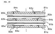
- glass-ceramic green sheets 81a, 81b, 81c, provided with viaholes 83a, 83b, 83c, and conductor patterns 84a, 84b, 84c, and ceramic green sheets 82a, 82b, each containing the above-described inorganic composition as a major component are alternately laminated, and fired under the firing conditions for the glass-ceramic green sheets, whereby a ceramic multilayer substrate is produced.
- perforations 85a, 85b are formed in the ceramic green sheets 82a, 82b containing the inorganic composition as a major component. No conductor material is filled into the perforations. That is, the thicknesses of the ceramic green sheets 82a, 82b are about 1 - 20 ⁇ m, or preferably 1 - 10 ⁇ m, and are extremely small as compared with those of the glass-ceramic green sheets 81a, 81b, 81c.
- the viaholes 83a, 83b, 83c formed in the glass-ceramic green sheets 81a, 81b, 81c enter the perforations 85a, 85b upon pressure-bonded or firing, so that the conductor patterns on the respective glass-ceramic green sheets are connected to each other.
- TABLE 1 shows the first experimental results.
- the experiment was carried out to investigate how different the heat shrinkage ratios in the plane direction at firing of the laminates are, depending on the thicknesses of the inorganic composition layers.
- the compositions and the layer structures of the glass-ceramic green sheets and the inorganic composition layers are the same as described in the above first embodiment.
- the sintering temperatures of the glass-ceramic green sheets is 1000°C
- the sintering temperature of the ceramic green sheets is 1500°C.
- the thickness of the glass-ceramic green sheets is 100 ⁇ m.
- the number of layers is 10.
- heat shrinkage ratio (%) 100 (longitudinal or lateral size of the bottom of the laminate after firing)/(longitudinal or lateral size of the bottom of the laminate before firing) thickness of inorganic composition layer ( ⁇ m) 0.0 0.5 1.0 5.0 10 15 20 25 shrinkage ratio (%) 83 95 97 98 98 98 98 NG
- NG signifies that peeling or cracking was generated, caused by the differences between the thermal expansion ratios of the ceramic green sheets and those of the glass-ceramic green sheets.
- the thicknesses of the inorganic composition layers are preferably set to be in the range of about 1 to 20 ⁇ m.
- TABLE 2 shows the second experimental results. This experiment was carried out to investigate how different the heat shrinkage ratios in the plane direction of the laminates caused when the glass-ceramic green sheets are fired depend on sintering temperatures.
- the glass-ceramic green sheets those having a sintering temperature of 1000°C were used, and the heat shrinkage ratios were calculated.
- the heat shrinkage ratios steeply decrease when the temperature becomes 900°C or higher.
- the heat shrinkage of the glass-ceramic green sheets progresses steeply when the temperature is about 100°C lower than the sintering temperature of 1000°C or higher, that is, about 900°C or higher. Accordingly the heat shrinkage in the plane direction of the glass-ceramic green sheets is inhibited if the ceramic green sheets are not heat shrunk in the range of 900°C to 1000°C.
- the object of the present invention can be achieved when the difference between the sintering temperatures of the glass-ceramic green sheets and the inorganic composition layers (or the ceramic green sheets containing the inorganic composition as a major component) is at least 100°C.
- the glass-ceramic green sheets each having the inorganic composition (ceramic green sheet) overlaid thereon are laminated in such a manner that the glass-ceramic green sheets and the inorganic compositions are alternately arranged to form the whole configuration of the laminate.
- the glass-ceramic green sheets, without the inorganic composition being interposed may be laminated for the configuration.
- the glass-ceramic green sheets and the inorganic composition layers may be formed separately, and the glass-ceramic green sheets and the ceramic green sheets each containing the inorganic composition as a major component may be laminated to form a laminate.
- a glass-ceramic green sheet having an inorganic composition on both faces but of different thicknesses can be employed as the undermost layer.
- conductor patterns and viaholes are formed in the respective layers constituting the laminate.
- a layer having no conductor pattern and or no viahole may be provided as a part of the laminate.
- a conductor is filled into the viaholes formed in the laminate.
- a conductor material may be provided only on the inner walls of the viaholes.
- a cavity may be formed in the laminate described in the third embodiment according to the points of the above-described second embodiment.
Landscapes
- Engineering & Computer Science (AREA)
- Chemical & Material Sciences (AREA)
- Ceramic Engineering (AREA)
- Inorganic Chemistry (AREA)
- Manufacturing & Machinery (AREA)
- Microelectronics & Electronic Packaging (AREA)
- Production Of Multi-Layered Print Wiring Board (AREA)
- Devices For Post-Treatments, Processing, Supply, Discharge, And Other Processes (AREA)
- Laminated Bodies (AREA)
Abstract
Description
| thickness of inorganic composition layer (µm) | 0.0 | 0.5 | 1.0 | 5.0 | 10 | 15 | 20 | 25 |
| shrinkage ratio (%) | 83 | 95 | 97 | 98 | 98 | 98 | 98 | NG |
| temperature (°C) | 700 | 800 | 900 | 925 | 950 | 975 | 1000 |
| shrinkage ratio (%) | 99.0 | 98.0 | 96.5 | 94.0 | 91.0 | 88.0 | 83.0 |
Claims (20)
- A method of producing a ceramic multilayer substrate which comprises laminating a plurality of glass-ceramic green sheets to form a laminate and firing the laminate;
wherein at least one surface of at least one glass-ceramic green sheet has a layer of inorganic composition whose sintering temperature is higher than that of the glass-ceramic green sheet thereon. - The method according to Claim 1, wherein one of the glass-ceramic green sheets has a smaller thickness than each of the other glass-ceramic green sheets and has said inorganic composition layer thereon and said one sheet is positioned so as to be an outermost layer of the laminate.
- The method according to Claim 2, wherein said one glass-ceramic green sheet having a smaller thickness is positioned so the inorganic composition thereon is disposed in the interior of the laminate.
- The method according to Claim 1, wherein a plurality of glass-ceramic green sheets having said inorganic composition layer thereon are positioned adjacent to one another to form said laminate.
- The method according to Claim 4, wherein at least one glass-ceramic green sheet does not have said inorganic composition layer thereon is employed in forming said laminate.
- The method according to Claim 1, wherein two glass-ceramic green sheets having a smaller thickness than each of the other glass-ceramic green sheets are positioned so as to be the two outermost layers of the laminate.
- The method according to Claim 1, including the step of positioning a plurality of the glass-ceramic green sheets have an opening therein such that the openings aline to form a cavity in said laminate.
- The method according to Claim 1, wherein the inorganic composition comprises alumina.
- The method according to Claim 1, wherein each inorganic composition layer on a glass-ceramic green sheet has a thickness of from about 1 to 20 µm.
- The method according to Claim 1, wherein each inorganic composition layer on a glass-ceramic green sheet has a thickness of from 1 to 10 µm.
- The method according to Claim 1, wherein the glass-ceramic green sheet and inorganic composition are selected such that the difference between the sintering temperature of the glass-ceramic green sheets and the sintering temperature of the inorganic composition is at least about 100°C.
- The method according to Claim 1, including the steps of first forming one of a glass-ceramic green sheet or an inorganic composition layer on a carrier film, and then forming the other of the glass-ceramic green sheet and inorganic composition layer on the first formed layer.
- The method according to Claim 12, including the steps of forming a perforation through each of the carder film, the glass-ceramic green sheet and the inorganic composition layer,introducing a conductor material into the perforation to produce a filled viahole;forming a conductor pattern on the inorganic composition layer in electrical communication with the conductor material in said viahole;separating the glass-ceramic green sheet having the viahole and the inorganic composition layer from the carrier film, andlaminating the glass-ceramic green sheet thus obtained.
- The method according to Claim 12, including the steps of forming a perforation through each of the carder film, the glass-ceramic green sheet and the inorganic composition,separating the glass-ceramic green sheet having the perforation and the inorganic composition layer from the carrier film, andpositioning the glass-ceramic green sheet thus obtained adjacent to a glass-ceramic green sheet having a viahole filled with a conductor material during said lamination step.
- The method according to Claim 1, including the steps of forming one of said plurality of glass-ceramic green sheets so as to have a smaller thickness than each of the other glass-ceramic green sheets and forming an inorganic composition layer on the surface of said glass-ceramic green sheet having smaller thickness.
- The method according to Claim 1, including the step of laminating a glass-ceramic green sheet as the uppermost layer of the laminate.
- The method according to Claim 1, wherein each of the glass-ceramic green sheets comprise glass-ceramic, organic binder and plasticizer.
- The method according to Claim 17, wherein two glass-ceramic green sheets having a smaller thickness than each of the other glass-ceramic green sheets are positioned so as to be the two outermost layers of the laminate and wherein the glass-ceramic green sheet and inorganic composition are selected such that the difference between the sintering temperature of the glass-ceramic green sheets and the sintering temperature of the inorganic composition is at least about 100°C.
- The method according to Claim 18, including the step of positioning a plurality of the glass-ceramic green sheets having said inorganic composition layer thereon and having an opening therein such that the openings aline to form a cavity in said laminate and at least a part of the cavity surface comprises an inorganic composition layer.
- The method according to Claim 19, wherein the inorganic composition comprises alumina and wherein each inorganic composition layer on a glass-ceramic green sheet has a thickness of from about 1 to 20 µm.
Applications Claiming Priority (4)
| Application Number | Priority Date | Filing Date | Title |
|---|---|---|---|
| JP5558299 | 1999-03-03 | ||
| JP5558299 | 1999-03-03 | ||
| JP30708399A JP3656484B2 (en) | 1999-03-03 | 1999-10-28 | Manufacturing method of ceramic multilayer substrate |
| JP30708399 | 1999-10-28 |
Publications (3)
| Publication Number | Publication Date |
|---|---|
| EP1033749A2 true EP1033749A2 (en) | 2000-09-06 |
| EP1033749A3 EP1033749A3 (en) | 2003-08-06 |
| EP1033749B1 EP1033749B1 (en) | 2008-05-07 |
Family
ID=26396474
Family Applications (1)
| Application Number | Title | Priority Date | Filing Date |
|---|---|---|---|
| EP00104260A Expired - Lifetime EP1033749B1 (en) | 1999-03-03 | 2000-03-01 | Method and producing ceramic multilayer substrate |
Country Status (4)
| Country | Link |
|---|---|
| US (3) | US6432239B1 (en) |
| EP (1) | EP1033749B1 (en) |
| JP (1) | JP3656484B2 (en) |
| DE (1) | DE60038756D1 (en) |
Cited By (10)
| Publication number | Priority date | Publication date | Assignee | Title |
|---|---|---|---|---|
| EP1209734A2 (en) | 2000-11-27 | 2002-05-29 | Murata Manufacturing Co., Ltd. | Multilayered ceramic substrate and production method therefor |
| WO2003028085A3 (en) * | 2001-09-14 | 2003-11-06 | Epcos Ag | Method for producing a ceramic substrate |
| WO2004043692A1 (en) * | 2002-11-11 | 2004-05-27 | Epcos Ag | Ceramic multilayer substrate and method for the production thereof |
| US6743534B2 (en) | 2001-10-01 | 2004-06-01 | Heraeus Incorporated | Self-constrained low temperature glass-ceramic unfired tape for microelectronics and methods for making and using the same |
| EP1471041A1 (en) * | 2003-04-22 | 2004-10-27 | Yageo Corporation | Multilayer ceramic composition |
| US6893710B2 (en) | 2003-04-18 | 2005-05-17 | Yageo Corporation | Multilayer ceramic composition |
| EP1435651A3 (en) * | 2003-01-02 | 2007-07-04 | E.I. Du Pont De Nemours And Company | Process for the constrained sintering of asymetrically configured dielectric layers |
| US7691469B2 (en) | 2005-09-16 | 2010-04-06 | Murata Manufacturing Co., Ltd. | Ceramic multilayer substrate and method for manufacturing the same |
| US8541694B2 (en) | 2007-03-01 | 2013-09-24 | Murata Manufacturing Co., Ltd. | Multilayer wiring board |
| US8729802B2 (en) | 2010-01-28 | 2014-05-20 | Koninklijke Philips N.V. | Burner with reduced height and method of manufacturing a burner |
Families Citing this family (55)
| Publication number | Priority date | Publication date | Assignee | Title |
|---|---|---|---|---|
| JP3656484B2 (en) * | 1999-03-03 | 2005-06-08 | 株式会社村田製作所 | Manufacturing method of ceramic multilayer substrate |
| JP3633435B2 (en) * | 2000-04-10 | 2005-03-30 | 株式会社村田製作所 | Multilayer ceramic substrate, manufacturing method and designing method thereof, and electronic device |
| JP2002084065A (en) * | 2000-09-07 | 2002-03-22 | Murata Mfg Co Ltd | Multilayer ceramic substrate, method of manufacturing the same, and electronic device |
| JP2002368422A (en) * | 2001-04-04 | 2002-12-20 | Murata Mfg Co Ltd | Multilayer ceramic substrate and method of manufacturing the same |
| JP2002368421A (en) * | 2001-06-08 | 2002-12-20 | Murata Mfg Co Ltd | Multilayer ceramic board and method for manufacturing the same |
| US6627020B2 (en) * | 2001-08-31 | 2003-09-30 | International Business Machines Corporation | Method for sinter distortion control |
| JP2003110016A (en) * | 2001-09-28 | 2003-04-11 | Kobe Steel Ltd | Method for forming air metal wiring on semiconductor substrate |
| DE10150715A1 (en) * | 2001-10-13 | 2003-04-30 | Bosch Gmbh Robert | Green ceramic insert body, ceramic insert body, ceramic green body or composite body and the ceramic layer composite produced therewith |
| JP3716783B2 (en) * | 2001-11-22 | 2005-11-16 | 株式会社村田製作所 | Method for manufacturing ceramic multilayer substrate and semiconductor device |
| US7381283B2 (en) * | 2002-03-07 | 2008-06-03 | Yageo Corporation | Method for reducing shrinkage during sintering low-temperature-cofired ceramics |
| US6776861B2 (en) * | 2002-06-04 | 2004-08-17 | E. I. Du Pont De Nemours And Company | Tape composition and process for internally constrained sintering of low temperature co-fired ceramic |
| US6827800B2 (en) * | 2003-01-30 | 2004-12-07 | E. I. Du Pont De Nemours And Company | Process for the constrained sintering of asymmetrically configured dielectric layers |
| JP4110170B2 (en) * | 2003-02-13 | 2008-07-02 | 株式会社フジクラ | Multilayer substrate and manufacturing method thereof |
| CN100589680C (en) * | 2003-11-14 | 2010-02-10 | 株式会社村田制作所 | Conductive paste and multilayer ceramic substrate |
| US7332805B2 (en) * | 2004-01-06 | 2008-02-19 | International Business Machines Corporation | Electronic package with improved current carrying capability and method of forming the same |
| JP2005268692A (en) * | 2004-03-22 | 2005-09-29 | Mitsubishi Electric Corp | Multilayer substrate manufacturing method |
| US7279217B2 (en) * | 2004-05-24 | 2007-10-09 | Tdk Corporation | Multilayer ceramic device, method for manufacturing the same, and ceramic device |
| US7508062B2 (en) * | 2005-03-11 | 2009-03-24 | Lsi Corporation | Package configuration and manufacturing method enabling the addition of decoupling capacitors to standard package designs |
| WO2007004415A1 (en) | 2005-07-01 | 2007-01-11 | Murata Manufacturing Co., Ltd. | Multilayer ceramic substrate, process for producing the same and composite green sheet for production of multilayer ceramic substrate |
| CN100527923C (en) * | 2005-07-01 | 2009-08-12 | 株式会社村田制作所 | Multilayer ceramic substrate, method for making the same, and composite green sheet for making multilayer ceramic substrate |
| JP4557002B2 (en) * | 2005-07-01 | 2010-10-06 | 株式会社村田製作所 | MULTILAYER CERAMIC SUBSTRATE, MANUFACTURING METHOD THEREOF, AND COMPOSITE GREEN SHEET FOR PRODUCTION OF MULTILAYER CERAMIC SUBSTRATE |
| JP4826253B2 (en) * | 2005-12-30 | 2011-11-30 | 株式会社村田製作所 | Method for manufacturing ceramic multilayer substrate and ceramic multilayer substrate |
| WO2007094123A1 (en) * | 2006-02-14 | 2007-08-23 | Murata Manufacturing Co., Ltd. | Multilayered ceramic electronic component, multilayered ceramic substrate, and method for manufacturing multilayered ceramic electronic component |
| US7901761B1 (en) * | 2006-04-17 | 2011-03-08 | Alfred E. Mann Foundation For Scientific Research | Hermetic vias utilizing metal-metal oxides |
| JP4862893B2 (en) * | 2006-06-02 | 2012-01-25 | 株式会社村田製作所 | Multilayer ceramic electronic component and manufacturing method thereof |
| JP4826348B2 (en) * | 2006-06-08 | 2011-11-30 | 株式会社村田製作所 | Method for producing multilayer ceramic electronic component with protruding electrodes |
| JP4957117B2 (en) * | 2006-08-09 | 2012-06-20 | 株式会社村田製作所 | Method for producing multilayer ceramic substrate and composite green sheet for producing multilayer ceramic substrate |
| JP2008159725A (en) * | 2006-12-22 | 2008-07-10 | Kyocera Corp | Ceramic multilayer substrate and manufacturing method thereof |
| WO2008126661A1 (en) * | 2007-04-11 | 2008-10-23 | Murata Manufacturing Co., Ltd. | Multilayer ceramic substrate and process for producing the same |
| DE102007022336A1 (en) * | 2007-05-12 | 2008-11-20 | Semikron Elektronik Gmbh & Co. Kg | Power semiconductor substrate with metal contact layer and manufacturing method thereof |
| TWI362102B (en) * | 2007-07-11 | 2012-04-11 | Ind Tech Res Inst | Three-dimensional dice-stacking package structure and method for manufactruing the same |
| DE112008001956T5 (en) * | 2007-07-26 | 2010-06-17 | Murata Mfg. Co., Ltd., Nagaokakyo-shi | Multilayer ceramic substrate and method of making the same |
| WO2009069398A1 (en) * | 2007-11-30 | 2009-06-04 | Murata Manufacturing Co., Ltd. | Ceramic composite multilayer substrate, method for manufacturing ceramic composite multilayer substrate and electronic component |
| KR100891824B1 (en) * | 2007-12-06 | 2009-04-07 | 삼성전기주식회사 | Laminated ceramic package |
| JP2009252783A (en) * | 2008-04-01 | 2009-10-29 | Murata Mfg Co Ltd | Production method of ceramic multilayer substrate, and method for adjusting amount of warpage of ceramic multilayer substrate |
| CN104589738A (en) * | 2008-05-15 | 2015-05-06 | 株式会社村田制作所 | Multilayer ceramic substrate and method for producing the same |
| JP5402776B2 (en) * | 2010-03-30 | 2014-01-29 | 株式会社村田製作所 | Manufacturing method of metal base substrate |
| JP5693411B2 (en) * | 2010-11-02 | 2015-04-01 | 京セラ株式会社 | Manufacturing method of light emitting element mounting substrate |
| JP5777997B2 (en) * | 2011-03-07 | 2015-09-16 | 日本特殊陶業株式会社 | Wiring board for electronic component inspection apparatus and manufacturing method thereof |
| JP5798435B2 (en) | 2011-03-07 | 2015-10-21 | 日本特殊陶業株式会社 | Wiring board for electronic component inspection apparatus and manufacturing method thereof |
| JP2013033914A (en) * | 2011-06-27 | 2013-02-14 | Toshiba Corp | Semiconductor device |
| KR101506760B1 (en) * | 2011-08-31 | 2015-03-30 | 삼성전기주식회사 | Magnetic substrate and method for manufacturing magnetic substrate |
| CN203015273U (en) * | 2012-12-24 | 2013-06-19 | 奥特斯(中国)有限公司 | Printed circuit board |
| US10219384B2 (en) | 2013-11-27 | 2019-02-26 | At&S Austria Technologie & Systemtechnik Aktiengesellschaft | Circuit board structure |
| AT515101B1 (en) | 2013-12-12 | 2015-06-15 | Austria Tech & System Tech | Method for embedding a component in a printed circuit board |
| US11523520B2 (en) | 2014-02-27 | 2022-12-06 | At&S Austria Technologie & Systemtechnik Aktiengesellschaft | Method for making contact with a component embedded in a printed circuit board |
| AT515447B1 (en) | 2014-02-27 | 2019-10-15 | At & S Austria Tech & Systemtechnik Ag | Method for contacting a component embedded in a printed circuit board and printed circuit board |
| WO2018030192A1 (en) * | 2016-08-10 | 2018-02-15 | 株式会社村田製作所 | Ceramic electronic component |
| KR102170221B1 (en) * | 2019-03-06 | 2020-10-28 | 주식회사 와이컴 | Space transformer for probe card and method for manufacturing the same |
| JP7294530B2 (en) * | 2020-04-07 | 2023-06-20 | 株式会社村田製作所 | Multilayer substrate and manufacturing method thereof |
| US11963309B2 (en) | 2021-05-18 | 2024-04-16 | Mellanox Technologies, Ltd. | Process for laminating conductive-lubricant coated metals for printed circuit boards |
| US12004308B2 (en) * | 2021-05-18 | 2024-06-04 | Mellanox Technologies, Ltd. | Process for laminating graphene-coated printed circuit boards |
| US12221695B2 (en) | 2021-05-18 | 2025-02-11 | Mellanox Technologies, Ltd. | CVD system with flange assembly for facilitating uniform and laminar flow |
| US12163228B2 (en) | 2021-05-18 | 2024-12-10 | Mellanox Technologies, Ltd. | CVD system with substrate carrier and associated mechanisms for moving substrate therethrough |
| US12289839B2 (en) | 2021-05-18 | 2025-04-29 | Mellanox Technologies, Ltd. | Process for localized repair of graphene-coated lamination stacks and printed circuit boards |
Family Cites Families (33)
| Publication number | Priority date | Publication date | Assignee | Title |
|---|---|---|---|---|
| US5102720A (en) * | 1989-09-22 | 1992-04-07 | Cornell Research Foundation, Inc. | Co-fired multilayer ceramic tapes that exhibit constrained sintering |
| US5085720A (en) * | 1990-01-18 | 1992-02-04 | E. I. Du Pont De Nemours And Company | Method for reducing shrinkage during firing of green ceramic bodies |
| US5254191A (en) * | 1990-10-04 | 1993-10-19 | E. I. Du Pont De Nemours And Company | Method for reducing shrinkage during firing of ceramic bodies |
| US5055966A (en) * | 1990-12-17 | 1991-10-08 | Hughes Aircraft Company | Via capacitors within multi-layer, 3 dimensional structures/substrates |
| JP2803421B2 (en) * | 1991-12-12 | 1998-09-24 | 松下電器産業株式会社 | Method for manufacturing multilayer ceramic substrate |
| US5277724A (en) * | 1991-12-18 | 1994-01-11 | General Electric Co. | Method of minimizing lateral shrinkage in a co-fired, ceramic-on-metal circuit board |
| JP2812605B2 (en) | 1992-04-30 | 1998-10-22 | 松下電器産業株式会社 | Method for manufacturing multilayer ceramic substrate |
| US5370759A (en) * | 1992-05-20 | 1994-12-06 | Matsushita Electric Industrial Co., Ltd. | Method for producing multilayered ceramic substrate |
| JPH0661649A (en) * | 1992-08-07 | 1994-03-04 | Matsushita Electric Ind Co Ltd | Method for manufacturing multilayer ceramic substrate |
| US5456778A (en) * | 1992-08-21 | 1995-10-10 | Sumitomo Metal Ceramics Inc. | Method of fabricating ceramic circuit substrate |
| US5662755A (en) * | 1993-10-15 | 1997-09-02 | Matsushita Electric Industrial Co., Ltd. | Method of making multi-layered ceramic substrates |
| JPH07202438A (en) * | 1993-12-29 | 1995-08-04 | Sumitomo Kinzoku Ceramics:Kk | Production of multilayer ceramic circuit board |
| US5601672A (en) * | 1994-11-01 | 1997-02-11 | International Business Machines Corporation | Method for making ceramic substrates from thin and thick ceramic greensheets |
| US5581876A (en) * | 1995-01-27 | 1996-12-10 | David Sarnoff Research Center, Inc. | Method of adhering green tape to a metal support substrate with a bonding glass |
| WO1996039298A1 (en) * | 1995-06-06 | 1996-12-12 | Sarnoff Corporation | Method for the reduction of lateral shrinkage in multilayer circuit boards on a support |
| JPH0992983A (en) * | 1995-07-17 | 1997-04-04 | Sumitomo Kinzoku Electro Device:Kk | Manufacturing method of ceramic multilayer substrate |
| US5708570A (en) * | 1995-10-11 | 1998-01-13 | Hughes Aircraft Company | Shrinkage-matched circuit package utilizing low temperature co-fired ceramic structures |
| JP3780386B2 (en) * | 1996-03-28 | 2006-05-31 | 株式会社村田製作所 | Ceramic circuit board and manufacturing method thereof |
| US5800761A (en) * | 1996-10-08 | 1998-09-01 | International Business Machines Corporation | Method of making an interface layer for stacked lamination sizing and sintering |
| US5858145A (en) * | 1996-10-15 | 1999-01-12 | Sarnoff Corporation | Method to control cavity dimensions of fired multilayer circuit boards on a support |
| US5866240A (en) * | 1997-03-06 | 1999-02-02 | Sarnoff Corporation | Thick ceramic on metal multilayer circuit board |
| JP3601671B2 (en) * | 1998-04-28 | 2004-12-15 | 株式会社村田製作所 | Manufacturing method of composite laminate |
| US6228196B1 (en) * | 1998-06-05 | 2001-05-08 | Murata Manufacturing Co., Ltd. | Method of producing a multi-layer ceramic substrate |
| JP3547327B2 (en) * | 1998-11-02 | 2004-07-28 | 松下電器産業株式会社 | Manufacturing method of ceramic multilayer substrate |
| US6245171B1 (en) * | 1998-11-23 | 2001-06-12 | International Business Machines Corporation | Multi-thickness, multi-layer green sheet lamination and method thereof |
| US6258192B1 (en) * | 1999-02-10 | 2001-07-10 | International Business Machines Corporation | Multi-thickness, multi-layer green sheet processing |
| JP3656484B2 (en) * | 1999-03-03 | 2005-06-08 | 株式会社村田製作所 | Manufacturing method of ceramic multilayer substrate |
| US6139666A (en) * | 1999-05-26 | 2000-10-31 | International Business Machines Corporation | Method for producing ceramic surfaces with easily removable contact sheets |
| JP3687484B2 (en) * | 1999-06-16 | 2005-08-24 | 株式会社村田製作所 | Method for manufacturing ceramic substrate and unfired ceramic substrate |
| JP3601679B2 (en) * | 1999-07-27 | 2004-12-15 | 株式会社村田製作所 | Method for producing composite laminate |
| JP3666321B2 (en) * | 1999-10-21 | 2005-06-29 | 株式会社村田製作所 | Multilayer ceramic substrate and manufacturing method thereof |
| JP3633435B2 (en) * | 2000-04-10 | 2005-03-30 | 株式会社村田製作所 | Multilayer ceramic substrate, manufacturing method and designing method thereof, and electronic device |
| JP2002368422A (en) * | 2001-04-04 | 2002-12-20 | Murata Mfg Co Ltd | Multilayer ceramic substrate and method of manufacturing the same |
-
1999
- 1999-10-28 JP JP30708399A patent/JP3656484B2/en not_active Expired - Lifetime
-
2000
- 2000-02-16 US US09/504,919 patent/US6432239B1/en not_active Expired - Lifetime
- 2000-03-01 DE DE60038756T patent/DE60038756D1/en not_active Expired - Lifetime
- 2000-03-01 EP EP00104260A patent/EP1033749B1/en not_active Expired - Lifetime
-
2002
- 2002-04-17 US US10/123,162 patent/US20020157760A1/en not_active Abandoned
-
2003
- 2003-06-05 US US10/454,481 patent/US6815046B2/en not_active Expired - Lifetime
Cited By (12)
| Publication number | Priority date | Publication date | Assignee | Title |
|---|---|---|---|---|
| EP1209734A2 (en) | 2000-11-27 | 2002-05-29 | Murata Manufacturing Co., Ltd. | Multilayered ceramic substrate and production method therefor |
| EP1209734A3 (en) * | 2000-11-27 | 2005-03-16 | Murata Manufacturing Co., Ltd. | Multilayered ceramic substrate and production method therefor |
| WO2003028085A3 (en) * | 2001-09-14 | 2003-11-06 | Epcos Ag | Method for producing a ceramic substrate |
| US6743534B2 (en) | 2001-10-01 | 2004-06-01 | Heraeus Incorporated | Self-constrained low temperature glass-ceramic unfired tape for microelectronics and methods for making and using the same |
| US6949156B2 (en) | 2001-10-01 | 2005-09-27 | Heraeus Incorporated | Methods for making and using self-constrained low temperature glass-ceramic unfired tape for microelectronics |
| WO2004043692A1 (en) * | 2002-11-11 | 2004-05-27 | Epcos Ag | Ceramic multilayer substrate and method for the production thereof |
| EP1435651A3 (en) * | 2003-01-02 | 2007-07-04 | E.I. Du Pont De Nemours And Company | Process for the constrained sintering of asymetrically configured dielectric layers |
| US6893710B2 (en) | 2003-04-18 | 2005-05-17 | Yageo Corporation | Multilayer ceramic composition |
| EP1471041A1 (en) * | 2003-04-22 | 2004-10-27 | Yageo Corporation | Multilayer ceramic composition |
| US7691469B2 (en) | 2005-09-16 | 2010-04-06 | Murata Manufacturing Co., Ltd. | Ceramic multilayer substrate and method for manufacturing the same |
| US8541694B2 (en) | 2007-03-01 | 2013-09-24 | Murata Manufacturing Co., Ltd. | Multilayer wiring board |
| US8729802B2 (en) | 2010-01-28 | 2014-05-20 | Koninklijke Philips N.V. | Burner with reduced height and method of manufacturing a burner |
Also Published As
| Publication number | Publication date |
|---|---|
| US6432239B1 (en) | 2002-08-13 |
| EP1033749A3 (en) | 2003-08-06 |
| EP1033749B1 (en) | 2008-05-07 |
| US20030211302A1 (en) | 2003-11-13 |
| JP3656484B2 (en) | 2005-06-08 |
| DE60038756D1 (en) | 2008-06-19 |
| JP2000315864A (en) | 2000-11-14 |
| US20020157760A1 (en) | 2002-10-31 |
| US6815046B2 (en) | 2004-11-09 |
Similar Documents
| Publication | Publication Date | Title |
|---|---|---|
| EP1033749A2 (en) | Method and producing ceramic multilayer substrate | |
| EP0932500B1 (en) | Method to control cavity dimensions of fired multilayer circuit boards on a support | |
| US7833370B2 (en) | Method for manufacturing a ceramic multi-layered substrate | |
| US4645552A (en) | Process for fabricating dimensionally stable interconnect boards | |
| EP2023701B1 (en) | Method for manufacturing ceramic multilayer substrate | |
| JP3511982B2 (en) | Method for manufacturing multilayer wiring board | |
| US20030008182A1 (en) | Method of manufacturing ceramic multi-layer substrate, and unbaked composite laminated body | |
| JP3547327B2 (en) | Manufacturing method of ceramic multilayer substrate | |
| US6942833B2 (en) | Ceramic multilayer substrate manufacturing method and unfired composite multilayer body | |
| JP3003413B2 (en) | Method for manufacturing multilayer ceramic substrate | |
| US6488795B1 (en) | Multilayered ceramic substrate and method of producing the same | |
| US6221193B1 (en) | Defect reduction method for screened greensheets and article produced therefrom | |
| JP3167678B2 (en) | Multilayer ceramic substrate and method of manufacturing the same | |
| JP3994795B2 (en) | Multilayer ceramic electronic component and manufacturing method thereof | |
| JP3413880B2 (en) | Method for producing multilayer ceramic sintered body | |
| US7204900B1 (en) | Method of fabricating structures using low temperature cofired ceramics | |
| JP2002118194A (en) | Method for manufacturing ceramic multilayer board for flip-chip | |
| JP2002076628A (en) | Manufacturing method of glass ceramic substrate | |
| JP2008159725A (en) | Ceramic multilayer substrate and manufacturing method thereof | |
| JP2001339160A (en) | Method for producing ceramic multilayer wiring board | |
| JP2737652B2 (en) | Multilayer ceramic substrate and method of manufacturing the same | |
| JP2003224362A (en) | Manufacturing method of ceramic multilayer substrate | |
| JPH04288854A (en) | Ceramic substrate for mounting semiconductor and manufacture thereof | |
| JPH08298379A (en) | Method for manufacturing multilayer ceramic substrate | |
| JP2008159726A (en) | Multilayer wiring board |
Legal Events
| Date | Code | Title | Description |
|---|---|---|---|
| PUAI | Public reference made under article 153(3) epc to a published international application that has entered the european phase |
Free format text: ORIGINAL CODE: 0009012 |
|
| 17P | Request for examination filed |
Effective date: 20000301 |
|
| AK | Designated contracting states |
Kind code of ref document: A2 Designated state(s): AT BE CH CY DE DK ES FI FR GB GR IE IT LI LU MC NL PT SE |
|
| AX | Request for extension of the european patent |
Free format text: AL;LT;LV;MK;RO;SI |
|
| PUAL | Search report despatched |
Free format text: ORIGINAL CODE: 0009013 |
|
| AK | Designated contracting states |
Designated state(s): AT BE CH CY DE DK ES FI FR GB GR IE IT LI LU MC NL PT SE |
|
| AX | Request for extension of the european patent |
Extension state: AL LT LV MK RO SI |
|
| 17Q | First examination report despatched |
Effective date: 20040121 |
|
| AKX | Designation fees paid |
Designated state(s): DE FI SE |
|
| 17Q | First examination report despatched |
Effective date: 20040121 |
|
| RAP1 | Party data changed (applicant data changed or rights of an application transferred) |
Owner name: MURATA MANUFACTURING CO., LTD. |
|
| GRAP | Despatch of communication of intention to grant a patent |
Free format text: ORIGINAL CODE: EPIDOSNIGR1 |
|
| GRAS | Grant fee paid |
Free format text: ORIGINAL CODE: EPIDOSNIGR3 |
|
| GRAA | (expected) grant |
Free format text: ORIGINAL CODE: 0009210 |
|
| AK | Designated contracting states |
Kind code of ref document: B1 Designated state(s): DE FI SE |
|
| REF | Corresponds to: |
Ref document number: 60038756 Country of ref document: DE Date of ref document: 20080619 Kind code of ref document: P |
|
| PG25 | Lapsed in a contracting state [announced via postgrant information from national office to epo] |
Ref country code: FI Free format text: LAPSE BECAUSE OF FAILURE TO SUBMIT A TRANSLATION OF THE DESCRIPTION OR TO PAY THE FEE WITHIN THE PRESCRIBED TIME-LIMIT Effective date: 20080507 |
|
| PG25 | Lapsed in a contracting state [announced via postgrant information from national office to epo] |
Ref country code: SE Free format text: LAPSE BECAUSE OF FAILURE TO SUBMIT A TRANSLATION OF THE DESCRIPTION OR TO PAY THE FEE WITHIN THE PRESCRIBED TIME-LIMIT Effective date: 20080807 |
|
| PLBE | No opposition filed within time limit |
Free format text: ORIGINAL CODE: 0009261 |
|
| STAA | Information on the status of an ep patent application or granted ep patent |
Free format text: STATUS: NO OPPOSITION FILED WITHIN TIME LIMIT |
|
| 26N | No opposition filed |
Effective date: 20090210 |
|
| PGFP | Annual fee paid to national office [announced via postgrant information from national office to epo] |
Ref country code: DE Payment date: 20190321 Year of fee payment: 20 |
|
| REG | Reference to a national code |
Ref country code: DE Ref legal event code: R071 Ref document number: 60038756 Country of ref document: DE |