EP1032122A2 - Verzerrungsausgleichsvorrichtung - Google Patents
Verzerrungsausgleichsvorrichtung Download PDFInfo
- Publication number
- EP1032122A2 EP1032122A2 EP00301419A EP00301419A EP1032122A2 EP 1032122 A2 EP1032122 A2 EP 1032122A2 EP 00301419 A EP00301419 A EP 00301419A EP 00301419 A EP00301419 A EP 00301419A EP 1032122 A2 EP1032122 A2 EP 1032122A2
- Authority
- EP
- European Patent Office
- Prior art keywords
- distortion
- order distortion
- amplifier
- terminal
- fixed resistor
- Prior art date
- Legal status (The legal status is an assumption and is not a legal conclusion. Google has not performed a legal analysis and makes no representation as to the accuracy of the status listed.)
- Withdrawn
Links
Images


Classifications
-
- H—ELECTRICITY
- H03—ELECTRONIC CIRCUITRY
- H03F—AMPLIFIERS
- H03F1/00—Details of amplifiers with only discharge tubes, only semiconductor devices or only unspecified devices as amplifying elements
- H03F1/32—Modifications of amplifiers to reduce non-linear distortion
- H03F1/3241—Modifications of amplifiers to reduce non-linear distortion using predistortion circuits
- H03F1/3276—Modifications of amplifiers to reduce non-linear distortion using predistortion circuits using the nonlinearity inherent to components, e.g. a diode
-
- H—ELECTRICITY
- H03—ELECTRONIC CIRCUITRY
- H03F—AMPLIFIERS
- H03F2200/00—Indexing scheme relating to amplifiers
- H03F2200/294—Indexing scheme relating to amplifiers the amplifier being a low noise amplifier [LNA]
-
- H—ELECTRICITY
- H03—ELECTRONIC CIRCUITRY
- H03F—AMPLIFIERS
- H03F2200/00—Indexing scheme relating to amplifiers
- H03F2200/372—Noise reduction and elimination in amplifier
Definitions
- the present invention relates to a distortion compensating device for compensating for a third-order distortion produced by an amplifier, and more particularly to a distortion compensating device which comprises a four-terminal power distributor connected to a third-order distortion generator and a phase adjuster for a size reduction.
- an amplifier generates high-order distortions when the amplifier amplifies a signal.
- a third-order distortion generated by the amplifier adversely affects the signal processing performed by the amplifier. If a signal having a certain frequency which is inputted to the amplifier is referred to as a fundamental signal, then the amplifier generates a third-order distortion depending on the fundamental signal, the third-order distortion having a frequency different from the frequency of the fundamental signal.
- One way of compensating a third-order distortion generated by an amplifier is to generate a distortion-compensating third-order distortion at a stage preceding the amplifier and cancel out the third-order distortion generated by the amplifier with the distortion-compensating third-order distortion.
- a distortion compensating device for generating such a distortion-compensating third-order distortion may combine a third-order distortion generated by a phase adjuster, for example, with a linear signal in an appropriate phase relationship and output the combined signal to a subsequent amplifier.
- Another distortion compensating device may comprise a third-order distortion generator and a wide-band phase unit.
- the conventional distortion compensating devices are large in scale and cannot be reduced in size because they have two separate signal processing systems, e.g., a signal processing system for processing an inputted fundamental signal and a signal processing system for generating a third-order distortion, and a separate combiner for combining output signals from the two signal processing systems, i.e., a fundamental signal and a third-order distortion signal.
- two separate signal processing systems e.g., a signal processing system for processing an inputted fundamental signal and a signal processing system for generating a third-order distortion
- a separate combiner for combining output signals from the two signal processing systems, i.e., a fundamental signal and a third-order distortion signal.
- the conventional distortion compensating devices need a wide-band LNA (Low Noise Amplifier) for amplifying a third-order distortion because a large signal loss occurs when the third-order distortion is generated.
- the conventional distortion compensating devices also require a complex external control circuit and a memory circuit for storing control information because a highly accurate control process is necessary for generating a third-order distortion suitable for distortion compensation.
- Another object of the present invention is to provide a distortion compensating device having a reduced power requirement.
- a distortion compensating device for compensating for a third-order distortion generated by an amplifier, comprising a power distributor having a first terminal for supplying an input signal to be inputted to an amplifier or being supplied with an input signal from an amplifier, a second terminal, and a third terminal, a third-order distortion generator connected to the second terminal for generating a third-order distortion having an amplitude for canceling out a third-order distortion generated by the amplifier depending on the supplied input signal, and a phase adjuster connected to the third terminal for adjusting the phase of the input signal to set the phase difference between the input signal and the third-order distortion generated by the third-order distortion generator to a phase difference for canceling out the third-order distortion generated by the amplifier, the power distributor having a fourth terminal for combining and outputting the third-order distortion generated by the third-order distortion generator and the input signal whose phase is adjusted by the phase adjuster.
- the distortion compensating device may comprise a coupler unit having such a coupler, and can be reduced in size. Specific examples for setting up the amplitude of the third-order distortion generated by the third-order distortion generator and also setting up the phase difference to be adjusted by the phase adjuster will be described later on with reference to preferred embodiments of the present invention.
- the distortion compensating device If the first terminal supplies the input signal to be inputted to the amplifier, then the distortion compensating device is positioned at a stage preceding the amplifier and supplies the input signal from the first terminal to the amplifier. If the first terminal is supplied with the input signal from the amplifier, then the distortion compensating device is positioned at a stage following the amplifier and is supplied with the input terminal outputted from the amplifier from the first terminal. At any rate, the distortion compensating device generates the third-order distortion for canceling the third-order distortion generated by the amplifier thereby to compensate for the third-order distortion generated by the amplifier.
- the distortion compensating device may be used to compensate for third-order distortions generated by more than one amplifier.
- the distortion compensating device may be arranged to compensate for third-order distortions generated by either a plurality of amplifiers preceding the distortion compensating device or a plurality of amplifiers following the distortion compensating device.
- the distortion compensating device may be arranged to compensate for a third-order distortion generated by at least one amplifier preceding the distortion compensating device and a third-order distortion generated by at least one amplifier following the distortion compensating device.
- the distortion compensating device In order for the distortion compensating device to compensate for third-order distortions generated by a plurality of amplifiers, the distortion compensating device generates a third-order distortion capable of canceling the sum of the third-order distortions generated by the amplifiers.
- the principles of the present invention are therefore applicable to the compensation for a third-order distortion generated by a single amplifier or third-order distortions generated by plural amplifiers.
- the distortion compensating device may be incorporated in a communication unit of a portable telephone system for compensating for a third-order distortion generated by an amplifier in the communication unit, or a communication unit of a W-CDMA system for compensating for a third-order distortion generated by an amplifier in the communication unit.
- the communication unit may comprise a base station or a terminal.
- FIG. 1 shows in block form a distortion compensating device according to a first embodiment of the present invention.
- the distortion compensating device comprises a 3dB coupler Q having four terminals including an input terminal T1, an output terminal T2, a 90. terminal, and a 0. terminal.
- the distortion compensating device also has a third-order distortion generator Z1 connected to the 90. terminal and comprising a semiconductor active element for generating a third-order distortion, and a phase adjuster Z2 connected to the 0. terminal for adjusting the phase of an input signal from the input terminal T1.
- the distortion compensating device is used in each of portable telephone base stations and portable telephone terminals of a portable communication system.
- the distortion compensating device serves to compensate for a third-order distortion generated by an amplifier in each of the portable telephone base stations and the portable telephone terminals.
- the distortion compensating device is disposed in a stage which precedes an amplifier that generates a third-order distortion to be compensated for, and a fundamental signal, i.e., a high-frequency signal transmitted from a portable telephone terminal or the like, applied to the amplifier is supplied from the input terminal T1.
- a fundamental signal i.e., a high-frequency signal transmitted from a portable telephone terminal or the like
- An example in which the distortion compensating device is disposed in a stage which follows an amplifier will be described later on with reference to FIG. 7.
- the third-order distortion generator Z1 When a fundamental signal is supplied from the input terminal T1, the third-order distortion generator Z1 generates a third-order distortion, and the phase adjuster Z2 adjusts the phase of the supplied fundamental signal.
- the 3dB coupler Q combines a reflected wave of the third-order distortion generated by the third-order distortion generator Z1 and the phase-adjusted fundamental signal with each other, and outputs the combined signal from the output terminal T2.
- the supplied signal wave is fully reflected.
- the 3dB coupler Q can now output the fundamental signal supplied from the input terminal T1 from the output terminal T2 with an ideal efficiency.
- a terminal T3 of the third-order distortion generator Z1 and a terminal T5 of the phase adjuster 2 are short-circuited or opened.
- the 3dB coupler Q is capable of removing an even-numbered-order distortion when such an even-numbered-order distortion is parasitically generated together with the third-order distortion by the third-order distortion generator Z1, and is also capable of removing an unwanted signal component such as a leakage wave from another system (e.g., a communication system) or a local signal.
- the distortion compensating device has a control voltage terminal T4 for controlling the amplitude of a third-order distortion generated by the third-order distortion generator Z1 and a control voltage terminal T5 for controlling the phase difference between the fundamental signal and the third-order distortion.
- the amplitude ratio and phase difference between the third-order distortion and the fundamental signal can be controlled depending on the magnitudes of DC voltages applied to the control voltage terminals T4, T6. Any variation in a signal loss as it passes through the distortion compensating device is small and stable even when the DC voltages applied to the control voltage terminals T4, T6 change.
- FIG. 2 shows a circuit arrangement of the distortion compensating device according to the first embodiment.
- a 3dB coupler Q1, an input terminal (IN) P1, a 90. terminal P2, a 0. terminal P3, an output terminal (ISO) P4, and a control voltage terminal P5 of the third-order distortion generator are identical to the 3dB coupler Q, the input terminal T1, the 90. terminal, the 0. terminal, the output terminal T2, and the control voltage terminal T4, respectively, shown in FIG. 1.
- a control voltage terminal of the phase adjuster is omitted from illustration.
- the 3dB coupler Q1 serves as a power distributor having four terminals.
- the input terminal P1 serves as a first terminal for supplying a signal to an amplifier or being supplied with a signal from an amplifier.
- the 90. terminal P2 serves as a second terminal associated with the third-order distortion generator for generating a third-order distortion depending on an input signal.
- the 0. terminal P3 serves as a third terminal associated with the phase adjuster for adjusting the phase of the input terminal.
- the 0. terminal P3 serves as a third terminal associated with the phase adjuster for adjusting the phase of an input signal.
- the output terminal P4 serves as a fourth terminal for combining a third-order distortion generated by the third-order distortion generator and an input signal whose phase has been adjusted by the phase ajuster, and outputting the combined signal.
- the third-order distortion generator connected to the 90. terminal P2 will be described below.
- the third-order distortion generator comprises a fixed resistor R1 connected to the 90. terminal P2, a capacitor C1 connected in series with the fixed resistor R1, two diode assemblies D1, D2 connected to the capacitor C1 parallel to each other in opposite directions, two capacitors C2, C3 connected in series with the diode assemblies D1, D2, respectively, a fixed resistor R2 connecting the capacitors C2, C3 to ground, a fixed resistor R3 connected between the diode assembly Dd1 and the capacitor C2, a capacitor C4 connecting the fixed resistor R3 to ground, and a fixed resistor R4 connecting the junction between the diode assembly D2 and the capacitor C3 to ground.
- the control voltage terminal P5 is connected to the diode assembly D1 through the fixed resistor R3.
- the fixed resistor R1 serves as a first fixed resistor, the capacitor C1 as a first capacitor, the two diode assemblies D1, D2 as two diode assemblies, the capacitor C2 as a second capacitor, the capacitor C3 as a third capacitor, the fixed resistor R2 as a second fixed resistor, the fixed resistor R3 as a third fixed resistor, the capacitor C4 as a fourth capacitor, and the fixed resistor R4 as a fourth fixed resistor.
- the fixed resistor R1 is a matching resistor for matching the impedances of the 90. terminal P2 and the third-order distortion generator.
- the three capacitors C1 - C3 are DC voltage blocking capacitors for blocking DC voltages and for being short-circuited at high frequencies.
- the fixed resistor R2 comprises a resistor which is terminated or opened at high frequencies.
- Each of the diode assemblies D1, D2 comprises a pair of series-connected Schottky barrier diodes or the like that act as distortion generating elements. When a high-frequency signal is supplied to the diode assemblies D1, D2, the Schottky barrier diodes or the like generate a third-order distortion.
- the two resistors R3, R4 which are open at high frequencies and the capacitor C4 which blocks high frequencies jointly make up a bias circuit for the diode assemblies D1, D2.
- the bias circuit is open at high frequencies or blocks high frequencies.
- diode assemblies D1, D2 connected parallel to each other in opposite directions
- only a single diode assembly may be connected to the capacitor C1.
- the diode assemblies D1, D2 connected parallel to each other in opposite directions are preferable because they can reduce characteristic variations due to temperature changes.
- the number of diodes of each of the diode assemblies D1, D2 is not limited to any number, but may be determined based on the electric power applied thereto, the amplitude ratio between a required output wave and a third-order distortion, etc.
- the diode assemblies D1, D2 When a fundamental signal is supplied from the input terminal P1 to the 90. terminal P2, the diode assemblies D1, D2 generate a third-order distortion depending on the supplied fundamental signal. A reflected wave containing the generated third-order distortion is outputted to the output terminal P4. The amplitude of only the generated third-order distortion can variably be controlled by controlling a DC voltage supplied from the control voltage terminal P5.
- the third-order distortion generated by the third-order distortion generator has an amplitude set to a level for canceling out the third-order distortion generated by the amplifier which is to be compensated for.
- the amplitude ratio between the fundamental signal inputted to the distortion compensating device and the third-order distortion generated by the distortion compensating device is set to the same value as the amplitude ratio between the fundamental signal inputted to the amplifier whose third-order distortion is to be compensated for and the third-order distortion generated by the amplifier, for thereby meeting the amplitude requirements for canceling out the third-order distortion generated by the amplifier.
- the amplitude of the third-order distortion generated by the third-order distortion generator may be set to an arbitrary level depending on the required accuracy of distortion compensation.
- phase adjuster connected to the 0. terminal P3 will be described below.
- the phase adjuster comprises a fixed resistor R5 and a variable capacitor C5 which are connected parallel to each other and to the 0. terminal P3, and an inductor I connected in series to the variable capacitor C5. Ends of the fixed resistor R5 and the variable capacitor C5 remote from the 0. terminal P3 are grounded.
- the fixed resistor R5 comprises a resistor having a resistance of 100 k., for example, which is open at high frequencies.
- the parallel-connected circuit of the fixed resistor R5 and the variable capacitor C5 is open at a wide range of frequencies.
- the variable capacitor C5 comprises a variable-capacitance diode, for example, and may be in the form of a trimmer capacitor, for example.
- the phase adjuster is capable of adjusting the phase of only a fundamental signal due to resonance depending on the combined reactance of the variable capacitor C5 and the inductor I which are connected in series with each other. Specifically, when a fundamental signal is supplied from the input terminal P1 to the 0. terminal P3, the phase adjuster adjusts the phase of only the fundamental signal to adjust the phase difference between the fundamental signal and the third-order distortion generated by the third-order distortion generator.
- the phase adjuster can output a reflected wave of the phase-adjusted fundamental signal to the output terminal P4.
- the phase adjuster can also variably control the phase difference between the fundamental signal and the third-order distortion by controlling the capacitance of the variable capacitor C5 with the DC voltage applied from the control voltage terminal (not shown).
- the phase difference adjusted by the phase difference is set to a value for canceling out the third-order distortion generated by the amplifier which is to be compensated for.
- the phase difference between the fundamental signal and the third-order distortion, which is outputted from the distortion compensating device is selected to be 180. out of phase with the phase difference between the fundamental signal inputted to the amplifier whose third-order distortion is to be compensated for and the third-order distortion generated by the amplifier, for thereby meeting the phase difference requirements for canceling out the third-order distortion generated by the amplifier.
- phase difference of the third-order distortion with the fundamental signal in the amplifier is ⁇
- the phase difference of the third-order distortion with the fundamental signal in the distortion compensating device may be set to ( ⁇ + 180.).
- the phase difference adjusted by the phase adjuster may be set to an arbitrary level depending on the required accuracy of distortion compensation.
- the distortion compensating device is able to generate a third-order distortion for canceling out the third-order distortion generated by the amplifier.
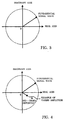
- FIGS. 3 through 6 The amplitudes and phases of a fundamental signal and a third-order distortion at the terminals P1 - P4 in a distortion compensating process carried out by the distortion compensating device are shown in FIGS. 3 through 6.
- the fundamental signal and the third-order distortion are represented by vectors in a complex plane, and the lengths of the vectors indicate amplitudes and the angles of the vectors indicate phases.
- FIG. 3 shows, by way of example, a fundamental signal applied to the input terminal P1 of the 3dB coupler Q1.
- the fundamental signal shown in FIG. 3 is applied to the input terminal P1.
- FIG. 4 shows, by way of example, a reflected wave of a third-order distortion at the 90. terminal P2 of the 3dB coupler Q1 and the fundamental signal.
- the amplitude of the third-order distortion can variably be controlled.
- FIG. 5 shows, by way of example, a reflected wave of the fundamental signal at the 0. terminal P3 of the 3dB coupler Q1.
- the phase of the fundamental signal can variably controlled and rotated.
- FIG. 6 shows, by way of example, the fundamental signal outputted from the output terminal P4 of the 3dB coupler Q1 and the third-order distortion.
- the distortion compensating device can set the amplitude ratio and the phase difference between the fundamental signal and the third-order distortion to arbitrary levels.
- the third-order distortion generator generates a third-order distortion having an amplitude for canceling a third-order distortion generated by an amplifier depending on an input signal (fundamental signal), and the phase adjuster adjusts the phase of the input signal (fundamental signal) to set the phase difference between the input signal and the third-order distortion generated by the third-order distortion generator to a phase difference for canceling out the third-order distortion generated by the amplifier.
- the generated third-order distortion and the phase-adjusted input signal are combined with each other, and the combined signal is outputted from the output terminal P4 for compensating for the third-order distortion generated by the amplifier.
- the distortion compensating device When the power consumption by an amplifier is lowered, the intercept point IP3 of the amplifier is lowered, i.e., the proportion of a third-order distortion contained in an input signal of the amplifier is increased. If the distortion compensating device according to the present invention is used to compensate for the third-order distortion, then the apparent intercept point IP3 can be increased, i.e., the proportion of the third-order distortion contained in the output signal of the amplifier can be reduced. Thus, even if an amplifier having a low output saturation level is employed, a high-frequency low-distortion amplifier can be realized, with the result that the amplifier can be reduced in size, power requirements, and cost.
- the extent to which the third-order distortion generated by the amplifier can be compensated for i.e., the distortion improvement level, varies by controlling the DC voltages applied to the control voltage terminals of the third-order distortion generator and the phase adjuster.
- the distortion compensating device can achieve a distortion improvement level of about 6 dB at all times.
- Such a distortion improvement level is equivalent to an increase by 3 dB of the intercept point IP3, making it possible to reduce the power requirements of the amplifier to about half the power requirements which would have to be satisfied if no distortion compensation were carried out.
- the distortion compensating device can remove (attenuate) signals in frequency bands other than the fundamental signal and the third-order distortion even when an even-numbered-order distortion is generated by the diode assemblies D1, D2. Therefore, the generated even-numbered-order distortion can be removed.
- the illustrated arrangement of the embodiment is effective to greatly reduce the power consumption (substantially to zero, for example) by the third-order distortion generator connected to the 90. terminal P2 and the phase adjuster connected to the 0. terminal P3, and to output the applied fundamental signal with a small attenuation, so that the power requirements of the distortion compensating device can greatly be reduced.
- the third-order distortion generated by the diode assemblies D1, D2 of the third-order distortion generator is 180. out of phase with the third-order distortion generated by the amplifier which is to be compensated for. Therefore, the phase of the fundamental signal may not variably be controlled by the phase adjuster.
- the phase of the fundamental signal to be varied by the phase adjuster may be of a fixed value.
- the phase adjuster may output the phase of the applied fundamental signal without varying the phase, i.e., by adjusting the phase to the applied phase.
- the phase of the fundamental signal is variably controlled for the reason that a slight phase error caused by distortion characteristics inherent in actual Schottky barrier diodes and the amplifier to be compensated for should variably be adjusted for ideal distortion compensation.
- the amplitude of the third-order distortion generated by the third-order distortion generator may not necessarily be variably controlled.
- the amplitude of the third-order distortion generated by the third-order distortion generator may be of a fixed value insofar as it is set to a value capable of canceling out the third-order distortion generated by the amplifier which is to be compensated for.
- the distortion compensating device has the coupler associated with the third-order distortion generator and the phase adjuster. Consequently, the distortion compensating device may comprise a coupler unit having such a coupler, and can be reduced in size. If the reduced-size distortion compensating device is incorporated in a portable telephone terminal, then the portable telephone terminal can be reduced in weight and can easily be carried around. In addition, the power requirements of the distortion compensating device can be reduced.
- FIG. 7 shows in block form a signal processor which incorporates the distortion compensating device therein.
- the signal processor comprises an amplifier (AMP) 1, a distortion compensating device 2 according to the present invention, an amplifier (AMP) 3, an attenuator (ATT) 4, an amplifier (AMP) 5, an attenuator (ATT) 6, and an amplifier (AMP) 7.
- the amplifier 1 comprises a low-distortion amplifier, for example, and the amplifiers 3, 5, 7 comprise power amplifiers, for example.
- a frequency-converted modulated signal for example, is supplied from an input terminal N1 to the amplifier 1, is processed by and passes through the distortion compensating device 2, the amplifier 3, the attenuator 4, the amplifier 5, the attenuator 6, and the amplifier 7, and is outputted from an output terminal N2.
- the distortion compensating device 2 compensates for third-order distortions generated by the amplifiers 1, 3, 5, 7. Specifically, the distortion compensating device 2 generates and outputs a third-order distortion for canceling out the sum of the third-order distortions generated by the amplifiers 1, 3, 5, 7.
- FIGS. 8(a) through 8(f) schematically show spectrums of a fundamental signal (fundamental signal wave) and third-order distortions generated in the signal processor shown in FIG. 7 at respective positions (a) through (f) therein in the distortion compensating process carried out by the distortion compensating device 2.
- the horizontal axis represents a frequency and the vertical axis a signal intensity.
- signals of two frequencies in the frequency band of the modulated signal applied to the input terminal N1 are indicated as the fundamental signal.
- FIG. 8(a) shows the fundamental signal applied to the input terminal N1.
- FIG. 8(b) shows a signal outputted from the amplifier 1, including a third-order distortion generated by the amplifier 1 and the fundamental signal.
- FIG. 8(c) shows a signal outputted from the distortion compensating device 2, including a third-order distortion generated by the distortion compensating device 2, which is added to the third-order distortion outputted from the amplifier 1.
- FIG. 8(d) shows a signal outputted from the amplifier 3, including a third-order distortion generated by the amplifier 3, which is added to the third-order distortion outputted from the distortion compensating device 2.
- FIG. 8(e) shows a signal outputted from the amplifier 5, including a third-order distortion generated by the amplifier 5, which is added to the third-order distortion outputted from the amplifier 3.
- FIG. 8(f) shows a signal outputted from the amplifier 7 to the output terminal N2, including a third-order distortion generated by the amplifier 7, which is added to the third-order distortion outputted from the amplifier 5.
- the third-order distortion generated by the distortion compensating device 2 cancels out the third-order distortions generated by the amplifiers 1, 3, 5, 7, so that no third-order distortion will be outputted from the output terminal N2.
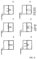
- a distortion compensating device according to a second embodiment of the present invention will be described below with reference to FIG. 9.
- the distortion compensating device according to the second embodiment is basically the same as the distortion compensating device according to the first embodiment as shown in FIG. 2 except for the structure of the phase adjuster connected to the 0. terminal P3. Therefore, only the phase adjuster of the distortion compensating device according to the second embodiment will be described below.
- the phase adjuster comprises a stub S connected to the 0. terminal P3 for rotating the phase of a fundamental signal, and a variable capacitor C6 connected to the stub S for varying the phase of the fundamental signal.
- An end of the variable capacitor C6 remote from its end connected to the stub S is grounded.
- the stub S may comprise an open stub or a short stub.
- the reactive component of the phase adjuster may become inductive or capacitive for adjusting the phase of only the fundamental signal.
- variable capacitor C6 should preferably comprise a trimmer capacitor.
- the variable capacitor C6 should preferably comprise a variable-capacitance capacitor whose capacitance can be varied under the control of an external voltage.
- the phase adjuster of the distortion compensating device according to the second embodiment is capable of adjusting the phase of only the fundamental signal.
- the distortion compensating device according to the second embodiment can variably control the phase difference between the fundamental signal and the third-order distortion by controlling the variable capacitor C6.
- a distortion compensating device according to a third embodiment of the present invention will be described below with reference to FIG. 10.
- the distortion compensating device according to the third embodiment is basically the same as the distortion compensating device according to the first embodiment as shown in FIG. 2 except for the structure of the phase adjuster connected to the 0. terminal P3. Therefore, only the phase adjuster of the distortion compensating device according to the third embodiment will be described below.
- the phase adjuster comprises a fixed resistor R6 and a variable capacitor C7 which are connected parallel to each other and to the 0. terminal P3. Ends of the fixed resistor R6 and the variable capacitor C7 which are remote from their ends connected to the 0. terminal P3 are connected to ground.
- the fixed resistor R6 comprises a resistor having a resistance of 100 k., for example, which is open at high frequencies.
- the parallel-connected circuit of the fixed resistor R6 and the variable capacitor C7 is open at a wide range of frequencies.
- the variable capacitor C7 comprises a variable-capacitance diode, for example, and may be in the form of a trimmer capacitor, for example.
- the phase adjuster of the distortion compensating device according to the third embodiment is capable of adjusting the phase of only the fundamental signal.
- the distortion compensating device according to the third embodiment can variably control the phase difference between the fundamental signal and the third-order distortion by controlling the variable capacitor C7.
- the third-order distortion generator is connected to the 90. terminal P2 of the 3dB coupler Q1, and the phase adjuster is connected to the 0. terminal P3 of the 3dB coupler Q1.
- the phase adjuster may be connected to the 90. terminal P2 of the 3dB coupler Q1, and the third-order distortion generator may be connected to the 0. terminal P3 of the 3dB coupler Q1.
- Such a modified distortion compensating device is also capable of generating and outputting a third-order distortion for compensating for the third-order distortion generated by the amplifier.
- the distortion compensating device is not limited to the structural details of the first through third embodiments, but may have different structural details.
- FETs or the like may be used as a device for generating a third-order distortion.
- the distortion compensating device can compensate for a third-order distortion generated by one or more amplifiers.
- the distortion compensating device according to the present invention should preferably be positioned at a stage preceding either a single amplifier whose third-order distortion is to be compensated for or the final one of plural amplifiers whose third-order distortions are to be compensated for.
- the distortion compensating device positioned at a stage following such an amplifier is also capable of compensating for a third-order distortion generated thereby.
- the distortion compensating device is incorporated in a portable telephone terminal or the like of a portable communication system.
- the principles of the present invention are also applicable to various fields where the third-order distortion generated by an amplifier is to be compensated for.
- the principles of the present invention are highly effective in a unit, such as a portable telephone terminal for W-CDMA communications, in which a signal in a wide frequency band is amplified by an amplifier because the compensation of the third-order distortion generated by the amplifier is particularly important.
- a distortion compensating device in accordance with the present invention may be used in combination with, for example, a feed-forward distortion-suppressed amplifier.
- Fig. 11 shows an example of the feed-forward distortion-suppressed amplifier.
- a coupler 11 distributes input signals to be amplified, and outputs one of the distributed signals to a main amplifier 12.
- the coupler 11 outputs the other distributed signal to a coupler 13 by way of a delay line 14.
- the main amplifier 12 amplifies the one distributed signal fed from the coupler 11, and outputs a resultant signal to the coupler 13.
- the coupler 13 synthesizes part of the amplified signal fed from the main amplifier 12 with the other distributed signal delayed while passing through the delay line 14.
- the coupler 13 acquires a distortion generated by the main amplifier 12 and outputs it to a sub amplifier 16.
- the coupler 13 outputs the other part of the amplified signal fed from the main amplifier 12 to a coupler 17 by way of a delay line 15.
- the sub amplifier 16 amplifies the distortion fed from the coupler 13 and outputs a resultant distortion to the coupler 17.
- the coupler 17 synthesizes the other part of the amplified signal, which has been amplified by the main amplifier 12 and delayed while passing through the delay line 15, with the distortion amplified by the sub amplifier 16 so as to minimize a distortion contained in the other part.
- the coupler 17 then outputs the distortion-minimized other part as a signal having undergone amplification.
- the foregoing main amplifier 12 and the foregoing sub amplifier 16 are generally formed by concatenating multiple stages of amplifiers each realized with an FET or the like.
- a distortion compensating device in accordance with the present invention may be included in, for example, the main amplifier 12 and used to compensate (for example, cancel) a third-order distortion generated by the main amplifier 12. Consequently, the main amplifier 12 can be reduced in size and in power requirements. Moreover, the level of a distortion to be input to the sub amplifier 16 is lowered. The sub amplifier 16 can therefore also be reduced in size and in power requirements. Eventually, the distortion compensating device can be reduced in size and in power requirements.
- a distortion compensating device in accordance with the present invention is, as mentioned above, adapted to the main amplifier 12. This makes it possible to lower the level of a third-order distortion generated by the main amplifier 12 by about 3 dB. Consequently, power (a distortion) output from the sub amplifier 16 can be minimized to approximately a half. Moreover, the main amplifier 12 and sub amplifier 16 can be, as mentioned above, reduced in size. The distortion compensating device can be reduced in size and improved in power efficiency. Eventually, the feed-forward distortion-suppressed amplifier can be reduced in size, and a digital portable telephone base station or the like to which the feed-forward distortion-suppressed amplifier is adapted can be reduced in size.
- a distortion compensating device in accordance with the present invention can be adapted not only to the foregoing main amplifier 12 but also to, for example, the sub amplifier 16.
- the distortion compensating device in accordance with the present invention may be included in the sub amplifier 16 and used to compensate (for example, cancel) a third-order distortion generated by the sub amplifier 16.
- Whether the distortion compensating device in accordance with the present invention is adapted to either or both of the main amplifier 12 and the sub amplifier 16 may be determined arbitrarily according to a use situation of the distortion compensating device.
Applications Claiming Priority (2)
| Application Number | Priority Date | Filing Date | Title |
|---|---|---|---|
| JP4605999 | 1999-02-24 | ||
| JP11046059A JP2000244252A (ja) | 1999-02-24 | 1999-02-24 | 歪み補償装置 |
Publications (2)
| Publication Number | Publication Date |
|---|---|
| EP1032122A2 true EP1032122A2 (de) | 2000-08-30 |
| EP1032122A3 EP1032122A3 (de) | 2004-07-14 |
Family
ID=12736454
Family Applications (1)
| Application Number | Title | Priority Date | Filing Date |
|---|---|---|---|
| EP00301419A Withdrawn EP1032122A3 (de) | 1999-02-24 | 2000-02-23 | Verzerrungsausgleichsvorrichtung |
Country Status (3)
| Country | Link |
|---|---|
| US (1) | US6271723B1 (de) |
| EP (1) | EP1032122A3 (de) |
| JP (1) | JP2000244252A (de) |
Families Citing this family (5)
| Publication number | Priority date | Publication date | Assignee | Title |
|---|---|---|---|---|
| US7657241B2 (en) | 2002-02-01 | 2010-02-02 | Qualcomm, Incorporated | Distortion reduction calibration |
| US6850115B2 (en) | 2002-08-26 | 2005-02-01 | Powerwave Technologies, Inc. | Enhanced efficiency LDMOS based feed forward amplifier |
| US7356309B2 (en) * | 2004-03-26 | 2008-04-08 | Broadcom Corporation | Directional coupler for communication system |
| JP2011160159A (ja) * | 2010-01-29 | 2011-08-18 | Toshiba Corp | 高周波電力増幅器および歪補償方法 |
| CN110057456A (zh) * | 2019-04-22 | 2019-07-26 | 北京科益虹源光电技术有限公司 | 一种用于准分子激光器的脉冲能量测量方法及测量电路 |
Citations (6)
| Publication number | Priority date | Publication date | Assignee | Title |
|---|---|---|---|---|
| US3825843A (en) * | 1973-06-08 | 1974-07-23 | Bell Telephone Labor Inc | Selective distortion compensation circuit |
| US4588958A (en) * | 1985-03-29 | 1986-05-13 | Rca Corporation | Adjustable reflective predistortion circuit |
| EP0475376A2 (de) * | 1990-09-12 | 1992-03-18 | General Instrument Corporation Of Delaware | Vorrichtung und Verfahren zur Linearisierung des Betriebs eines externen optischen Modulators |
| US5172068A (en) * | 1990-09-17 | 1992-12-15 | Amoco Corporation | Third-order predistortion linearization circuit |
| EP0552059A1 (de) * | 1992-01-16 | 1993-07-21 | Japan Radio Co., Ltd | Leistungsverstärkervorrichtung |
| US5304944A (en) * | 1992-10-09 | 1994-04-19 | Hughes Aircraft Company | High frequency linearizer |
Family Cites Families (4)
| Publication number | Priority date | Publication date | Assignee | Title |
|---|---|---|---|---|
| US4157508A (en) * | 1977-11-21 | 1979-06-05 | Bell Telephone Laboratories, Incorporated | Signal cuber circuit |
| US5850305A (en) * | 1996-12-18 | 1998-12-15 | Scientific-Atlanta, Inc. | Adaptive predistortion control for optical external modulation |
| US6122085A (en) * | 1997-04-08 | 2000-09-19 | Lucent Technologies Inc. | Lightwave transmission techniques |
| KR100296146B1 (ko) * | 1998-05-23 | 2001-08-07 | 오길록 | 소신호선형화장치 |
-
1999
- 1999-02-24 JP JP11046059A patent/JP2000244252A/ja active Pending
-
2000
- 2000-02-23 EP EP00301419A patent/EP1032122A3/de not_active Withdrawn
- 2000-02-24 US US09/512,331 patent/US6271723B1/en not_active Expired - Fee Related
Patent Citations (6)
| Publication number | Priority date | Publication date | Assignee | Title |
|---|---|---|---|---|
| US3825843A (en) * | 1973-06-08 | 1974-07-23 | Bell Telephone Labor Inc | Selective distortion compensation circuit |
| US4588958A (en) * | 1985-03-29 | 1986-05-13 | Rca Corporation | Adjustable reflective predistortion circuit |
| EP0475376A2 (de) * | 1990-09-12 | 1992-03-18 | General Instrument Corporation Of Delaware | Vorrichtung und Verfahren zur Linearisierung des Betriebs eines externen optischen Modulators |
| US5172068A (en) * | 1990-09-17 | 1992-12-15 | Amoco Corporation | Third-order predistortion linearization circuit |
| EP0552059A1 (de) * | 1992-01-16 | 1993-07-21 | Japan Radio Co., Ltd | Leistungsverstärkervorrichtung |
| US5304944A (en) * | 1992-10-09 | 1994-04-19 | Hughes Aircraft Company | High frequency linearizer |
Also Published As
| Publication number | Publication date |
|---|---|
| EP1032122A3 (de) | 2004-07-14 |
| JP2000244252A (ja) | 2000-09-08 |
| US6271723B1 (en) | 2001-08-07 |
Similar Documents
| Publication | Publication Date | Title |
|---|---|---|
| US5148117A (en) | Adaptive feed-forward method and apparatus for amplifier noise reduction | |
| US4581595A (en) | Phase shift network with minimum amplitude ripple | |
| US20020014920A1 (en) | High frequency power amplifier | |
| US3886470A (en) | Feed-forward amplifier system | |
| US4926136A (en) | Power amplifier combiner for improving linearity of an output | |
| EP1312159A2 (de) | Rückgekoppelte hochfrequenzverstärker | |
| CA2204409A1 (en) | Amplifier circuit and method of tuning the amplifier circuit | |
| WO2003030354A2 (en) | A spurious ratio control circuit for use with feed-forward linear amplifiers | |
| EP0552059A1 (de) | Leistungsverstärkervorrichtung | |
| US5939920A (en) | Method and apparatus which adds distortion to a signal to compensate for distortion added at a later stage by a nonlinear element | |
| US6753728B2 (en) | Distortion reducing circuit | |
| US6919774B2 (en) | Broadband PIN diode attenuator bias network | |
| US4157508A (en) | Signal cuber circuit | |
| US5258722A (en) | Amplifier circuit with distortion cancellation | |
| US6271723B1 (en) | Distortion compensating device | |
| US6400223B1 (en) | Double carrier cancellation in wide band multi-carrier feed forward linearized power amplifier | |
| EP1254507B1 (de) | Schaltung zur reduzierung der intermodulationsverzerrung zweiter und dritter ordnung eines breitbandhochfrequenzverstärkers | |
| US6650185B1 (en) | Frequency selective distributed amplifier | |
| US6424226B1 (en) | Two-port with a frequency-dependent network | |
| US6720829B2 (en) | Distortion-compensated amplifying circuit | |
| KR20220002302A (ko) | 잡음 제거 기능을 갖는 저잡음 증폭기 | |
| US6392481B1 (en) | Method and apparatus for improved fed forward amplification | |
| US9377796B2 (en) | Interference suppression for switched mode power supply | |
| US20030001670A1 (en) | Nonlinear feedback linearizer | |
| JP2003332852A (ja) | プリディストーション回路 |
Legal Events
| Date | Code | Title | Description |
|---|---|---|---|
| PUAI | Public reference made under article 153(3) epc to a published international application that has entered the european phase |
Free format text: ORIGINAL CODE: 0009012 |
|
| AK | Designated contracting states |
Kind code of ref document: A2 Designated state(s): AT BE CH CY DE DK ES FI FR GB GR IE IT LI LU MC NL PT SE |
|
| AX | Request for extension of the european patent |
Free format text: AL;LT;LV;MK;RO;SI |
|
| PUAL | Search report despatched |
Free format text: ORIGINAL CODE: 0009013 |
|
| AK | Designated contracting states |
Kind code of ref document: A3 Designated state(s): AT BE CH CY DE DK ES FI FR GB GR IE IT LI LU MC NL PT SE |
|
| AX | Request for extension of the european patent |
Extension state: AL LT LV MK RO SI |
|
| RIC1 | Information provided on ipc code assigned before grant |
Ipc: 7H 03F 3/60 B Ipc: 7H 03F 1/32 A |
|
| AKX | Designation fees paid | ||
| REG | Reference to a national code |
Ref country code: DE Ref legal event code: 8566 |
|
| STAA | Information on the status of an ep patent application or granted ep patent |
Free format text: STATUS: THE APPLICATION IS DEEMED TO BE WITHDRAWN |
|
| 18D | Application deemed to be withdrawn |
Effective date: 20050115 |
|
| REG | Reference to a national code |
Ref country code: HK Ref legal event code: WD Ref document number: 1032683 Country of ref document: HK |