EP1028518A2 - Soft-switching cell for reducing switching losses in pulse-width-modulated converters - Google Patents
Soft-switching cell for reducing switching losses in pulse-width-modulated converters Download PDFInfo
- Publication number
- EP1028518A2 EP1028518A2 EP00301054A EP00301054A EP1028518A2 EP 1028518 A2 EP1028518 A2 EP 1028518A2 EP 00301054 A EP00301054 A EP 00301054A EP 00301054 A EP00301054 A EP 00301054A EP 1028518 A2 EP1028518 A2 EP 1028518A2
- Authority
- EP
- European Patent Office
- Prior art keywords
- switch
- power converter
- boost
- current
- converter
- Prior art date
- Legal status (The legal status is an assumption and is not a legal conclusion. Google has not performed a legal analysis and makes no representation as to the accuracy of the status listed.)
- Granted
Links
Images


Classifications
-
- H—ELECTRICITY
- H03—ELECTRONIC CIRCUITRY
- H03K—PULSE TECHNIQUE
- H03K17/00—Electronic switching or gating, i.e. not by contact-making and –breaking
- H03K17/51—Electronic switching or gating, i.e. not by contact-making and –breaking characterised by the components used
- H03K17/56—Electronic switching or gating, i.e. not by contact-making and –breaking characterised by the components used by the use, as active elements, of semiconductor devices
-
- H—ELECTRICITY
- H02—GENERATION; CONVERSION OR DISTRIBUTION OF ELECTRIC POWER
- H02M—APPARATUS FOR CONVERSION BETWEEN AC AND AC, BETWEEN AC AND DC, OR BETWEEN DC AND DC, AND FOR USE WITH MAINS OR SIMILAR POWER SUPPLY SYSTEMS; CONVERSION OF DC OR AC INPUT POWER INTO SURGE OUTPUT POWER; CONTROL OR REGULATION THEREOF
- H02M1/00—Details of apparatus for conversion
- H02M1/42—Circuits or arrangements for compensating for or adjusting power factor in converters or inverters
- H02M1/4208—Arrangements for improving power factor of AC input
-
- H—ELECTRICITY
- H02—GENERATION; CONVERSION OR DISTRIBUTION OF ELECTRIC POWER
- H02M—APPARATUS FOR CONVERSION BETWEEN AC AND AC, BETWEEN AC AND DC, OR BETWEEN DC AND DC, AND FOR USE WITH MAINS OR SIMILAR POWER SUPPLY SYSTEMS; CONVERSION OF DC OR AC INPUT POWER INTO SURGE OUTPUT POWER; CONTROL OR REGULATION THEREOF
- H02M3/00—Conversion of DC power input into DC power output
- H02M3/02—Conversion of DC power input into DC power output without intermediate conversion into AC
- H02M3/04—Conversion of DC power input into DC power output without intermediate conversion into AC by static converters
- H02M3/10—Conversion of DC power input into DC power output without intermediate conversion into AC by static converters using discharge tubes with control electrode or semiconductor devices with control electrode
- H02M3/145—Conversion of DC power input into DC power output without intermediate conversion into AC by static converters using discharge tubes with control electrode or semiconductor devices with control electrode using devices of a triode or transistor type requiring continuous application of a control signal
- H02M3/155—Conversion of DC power input into DC power output without intermediate conversion into AC by static converters using discharge tubes with control electrode or semiconductor devices with control electrode using devices of a triode or transistor type requiring continuous application of a control signal using semiconductor devices only
- H02M3/156—Conversion of DC power input into DC power output without intermediate conversion into AC by static converters using discharge tubes with control electrode or semiconductor devices with control electrode using devices of a triode or transistor type requiring continuous application of a control signal using semiconductor devices only with automatic control of output voltage or current, e.g. switching regulators
- H02M3/158—Conversion of DC power input into DC power output without intermediate conversion into AC by static converters using discharge tubes with control electrode or semiconductor devices with control electrode using devices of a triode or transistor type requiring continuous application of a control signal using semiconductor devices only with automatic control of output voltage or current, e.g. switching regulators including plural semiconductor devices as final control devices for a single load
-
- H—ELECTRICITY
- H03—ELECTRONIC CIRCUITRY
- H03K—PULSE TECHNIQUE
- H03K17/00—Electronic switching or gating, i.e. not by contact-making and –breaking
- H03K17/13—Modifications for switching at zero crossing
-
- H—ELECTRICITY
- H02—GENERATION; CONVERSION OR DISTRIBUTION OF ELECTRIC POWER
- H02M—APPARATUS FOR CONVERSION BETWEEN AC AND AC, BETWEEN AC AND DC, OR BETWEEN DC AND DC, AND FOR USE WITH MAINS OR SIMILAR POWER SUPPLY SYSTEMS; CONVERSION OF DC OR AC INPUT POWER INTO SURGE OUTPUT POWER; CONTROL OR REGULATION THEREOF
- H02M1/00—Details of apparatus for conversion
- H02M1/32—Means for protecting converters other than automatic disconnection
- H02M1/34—Snubber circuits
- H02M1/342—Active non-dissipative snubbers
-
- H—ELECTRICITY
- H03—ELECTRONIC CIRCUITRY
- H03K—PULSE TECHNIQUE
- H03K2217/00—Indexing scheme related to electronic switching or gating, i.e. not by contact-making or -breaking covered by H03K17/00
- H03K2217/0036—Means reducing energy consumption
-
- Y—GENERAL TAGGING OF NEW TECHNOLOGICAL DEVELOPMENTS; GENERAL TAGGING OF CROSS-SECTIONAL TECHNOLOGIES SPANNING OVER SEVERAL SECTIONS OF THE IPC; TECHNICAL SUBJECTS COVERED BY FORMER USPC CROSS-REFERENCE ART COLLECTIONS [XRACs] AND DIGESTS
- Y02—TECHNOLOGIES OR APPLICATIONS FOR MITIGATION OR ADAPTATION AGAINST CLIMATE CHANGE
- Y02B—CLIMATE CHANGE MITIGATION TECHNOLOGIES RELATED TO BUILDINGS, e.g. HOUSING, HOUSE APPLIANCES OR RELATED END-USER APPLICATIONS
- Y02B70/00—Technologies for an efficient end-user side electric power management and consumption
- Y02B70/10—Technologies improving the efficiency by using switched-mode power supplies [SMPS], i.e. efficient power electronics conversion e.g. power factor correction or reduction of losses in power supplies or efficient standby modes
Definitions
- the present invention relates to power converters.
- the present invention relates to pulse-width-modulated (PWM) converters.
- a continuous-conduction-mode boost converter is a preferred implementation of a front-end converter with active input-current shaping.
- the output voltage of such a boost input-current shaper is relatively high, since the DC output voltage of the boost converter must be higher than the peak input voltage. Due to this high output voltage, a fast-recovery boost rectifier is required.
- a fast-recovery rectifier produces a significant reverse-recovery-related loss when it is switched under a "hard-switching" condition.
- boost input-current-shapers are operated at relatively low switching frequencies to avoid a significant deterioration of their conversion efficiencies.
- switching frequency and, therefore, the power-density of the boost, front-end converter can be increased.
- Each of the references (a) - (d) above discloses an auxiliary active switch operating together with a few passive components (e.g., inductors and capacitors), thus forming an active snubber that is used to control the rate of change of rectifier current (di/dt) and to create conditions for zero-voltage switching (ZVS) of the main switch and the rectifier.
- Active snubbers are described, for example, in “Switched snubber for high frequency switching," (“Harada et al.") by K. Harada, H. Sakamoto, IEEE Power Electronics Specialists' Conf (PESC) Rec., pp. 181 - 188, Jun. 1990.
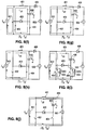
- Figs. 1 - 3 show the soft-switched boost circuit introduced in Hua et al., Bassett et al., and Jovanovic, respectively.
- the boost converter circuits proposed in Streit and Hua et al. use a snubber inductor connected to the common node of the boost switch and the rectifier to control the rate of change of rectifier current (di/dt).
- the main switch and the rectifier in the circuits proposed in Streit and Hua et al. possess minimum voltage and current stresses.
- the boost switch closes and the rectifier turns off under zero-voltage (soft-switching) conditions.
- the auxiliary switch operates under "hard” switching conditions, as it is closed while its voltage is equal to the output voltage, and subsequently opened while carrying a current greater than the input current.
- the rate of change of rectifier current is controlled by a snubber inductor connected in series with the boost switch and the rectifier. Because of this placement of the inductor, the voltage stress of the main switch is higher than that of the circuits described in Streit and Hua et al. This increased voltage stress can be minimized by a proper selection of the snubber-inductance value and the switching frequency, as taught in Jovanovic. Both the boost and the auxiliary switches in the circuits in Bassett et al. and Jovanovic, as well as the boost rectifier, operate under ZVS conditions.
- the major deficiency of the boost converters described in Streit and Hua et al. is a severe, undesirable resonance between the output capacitance C OSS of the auxiliary switch and the resonant inductor.
- the undesirable resonance occurs after the auxiliary switch is opened and the snubber inductor current falls to zero and adversely affects the operation of the circuit and must be eliminated.
- the resonance is eliminated by connecting a rectifier and a saturable inductor in series with the snubber inductor, as shown in Fig. 1, which degrades the conversion efficiency and increases both the component count and the cost of the circuit.
- the present invention provides a zero-current, zero-voltage-switched (ZC-ZVS) cell which includes a snubber inductor, a clamp diode, a clamp capacitor, a main switch, and an auxiliary switch.
- ZC-ZVS zero-current, zero-voltage-switched
- the ZC-ZVS cell reduces reverse-recovery-related losses of the boost rectifier and also provides lossless switching for the main and auxiliary switches.
- the ZC-ZVS cell of the present invention is applicable, for example, to soft-switched PWM boost converter.
- the reverse-recovery-related losses in the boost topology are reduced by the snubber inductor, which is connected in series with the main switch (boost switch) and the boost rectifier, and which controls the rate of current change (di/dt) in the boost rectifier during its turn-off.
- the main switch operates with zero-current and zero-voltage switching
- the auxiliary switch operates with zero-voltage switching.
- a proper operation of a circuit of the present invention requires overlapping gate drives of the main and the auxiliary switches where the main switch becomes conducting or non-conducting prior to the auxiliary switch becoming conducting or non-conducting.
- the snubber inductor controls the rate of change of the current in the boost rectifier to reduce reverse-recovery-related losses of the boost rectifier.
- the snubber inductor prevents the main-switch current from increasing immediately, the main switch becomes conducting with zero-current switching.
- the snubber inductor and the output capacitance of the auxiliary switch form a resonant circuit, so that the voltage across the auxiliary switch falls to zero by a resonant oscillation. As a result, the auxiliary switch becomes conducting when the voltage across it is zero.
- the snubber inductor and the clamp capacitor form yet another resonant circuit through the closed switches. Due to this resonance, the current through the main switch is reduced to zero prior to the main switch becoming non-conducting, while the voltage across the main switch is clamped to zero by the conducting clamp diode and the auxiliary switch. Thus, the main switch turns off with zero-current-zero-voltage switching.
- a non-isolated (direct) gate drive can be used.
- a circuit of the present invention is not susceptible to failures due to accidental transient overlapping of the main and auxiliary switch gate drives.
- the voltage and current stresses of the components in an active-snubber boost converter of the present invention are similar to those in conventional "hard-switched" converters. The same technique can be extended to any member of the PWM-converter family.
- Boost power stage 400 includes snubber inductor 401 (Ls), which is connected in series with main switch 402 (S) and boost rectifier 406. Snubber inductor 401 controls the rate of current change (di/dt) of boost rectifier 406.
- main or boost switch 402 snubber inductor 401, auxiliary switch 404 (S 1 ), clamp capacitor 405 (C C ), and clamp diode 403 (D C ) form a zero-current-zero-voltage-switched (ZC-ZVS) cell 450.
- ZC-ZVS zero-current-zero-voltage-switched
- boost inductor 408 is represented by a constant-current source 501 (I IN ). Further, since the output-ripple voltage is negligible, voltage V O across output filter capacitor 407 is represented by constant-voltage source 502.
- semiconductor devices e.g., switches 402 and 404
- switches 402 and 404 can be regarded as having zero resistance (i.e., short circuits). Output capacitances of switches 402 and 404, and the reverse-recovery charge of boost rectifier 406 are not neglected.
- Figs. 6(a)-6(j) show topological stages of boost power stage 400 of Fig. 4 during a switching cycle in which input current I IN is greater than the peak current (I LS(PK) ) of snubber inductor 401.
- Fig. 7 shows key waveforms of boost power stage 400 during the same switching cycle.
- the gate-drive waveforms i.e., waveforms 701 and 702, for gate driving signals G S and G S1 , respectively
- boost switch 402 and auxiliary switch 404 are overlapping (i.e., boost switch 402 and auxiliary switch 404 are both conducting for some time period).
- V S1 waveform 704 of auxiliary switch 404 at terminal 411 in Fig. 4 decreases from V O +V C to zero in a resonant fashion.
- ZVS zero-voltage switching
- boost switch 402 since the voltage stress of boost switch 402, auxiliary switch 404, and boost rectifier 406 is V O +V c , the voltage stress in boost switch 402 in boost power stage 400 is higher than in a conventional "hard-switched" boost converter by voltage V C .
- clamp voltage V C is carefully selected to keep the voltage stresses of boost switch 402 and auxiliary switch 404 within reasonable limits.
- I O I O(max)
- V IN V IN(max)
- clamp capacitor voltage V C can be minimized by minimizing the L s f S product.
- Figs. 8 and 9 show topological stages of boost power stage 400, in which input current I IN is less than the peak current (I LS(PK) ) in snubber inductor 401.
- Fig. 9 shows key waveforms of boost power stage 400, when input current I IN is less than the peak current (I LS(PK) ) in snubber inductor 401.
- the analysis provided above with respect to full load operation is equally applicable to the light load operations of Figs. 8(a)-8(j) and Fig. 9, and thus is not repeated.
- FIG. 10 shows desired input current waveform ( I REC / IN ) 1001, input voltage waveform ( V REC / IN ) 1002, and output voltage waveform (V O ) 1003 in an input-current-shaping application. Because in an input-current-shaping application, input voltage V IN varies during a line cycle, and output voltage V o is constant, the duty cycle of boost rectifier 406 varies from 0% to 100%. Moreover, when the instantaneous input voltage is near zero, the stored energy in boost inductor 408 may be insufficient to charge clamp capacitor 405.
- boost power stage 1100 of Fig. 11 is obtained by modifying boost power stage 400 of Fig. 4.
- Fig. 11 shows boost power stage 1100, including diode 1101 and resistor 1102 provided across clamp capacitor 405. Resistor 1102 is connected across clamp capacitor 405 to prevent excessive charging of clamp capacitor 405 when the duty cycle of boost power stage 1100 is at the minimum around the peaks of the line voltage.
- capacitor 1104 which is provided in parallel with auxiliary switch 404, optimizes the magnitude of current I + / C ( max ) so that boost switch 402 is opened under ZCS conditions.
- boost power stage 400 or boost power stage 1100 can be implemented in substantially same way as conventional "hard-switched" power converters, so long as an additional gate-driver circuit is provided.
- boost power stage 400 or boost power stage 1100 can be implemented with any known control technique, such as average-current, peak-current, or hysteretic control.
- boost switch 402 is provided by an IXGK50N60 IGBT; auxiliary, switch 404 is provided by a 2SK2837 MOSFET; boost rectifier 406 is provided by two RHRP3060 rectifiers connected in parallel; boost inductor 408 is provided by a 0.8 mH inductance; snubber inductor 401 is provided by a 4.7 ⁇ H inductor; snubber rectifier 403 is provided by a RHRP3060 rectifier, and filter capacitor 407 is provided by two 470 ⁇ F/450 V capacitors connected in parallel.
- Boost inductor 408 was built using Magnetics toroidal core (Kool Mu 77439-A7, two cores in parallel) and 55 turns of AWG#14 wire, and snubber inductor 403 was built with Magnetics toroidal core (MPP 55550-A2, two cores in parallel) with 9 turns of AWG#14 wire.
- the control circuit for the experimental circuit was implemented with an average-current PFC controller UC3854. TC4420 and TSC429 drivers are used to generate the required gate-drive signals for the boost switch 402 and auxiliary switch 404, respectively.
- Table 1 shows the measured efficiencies of the experimental converter with and without the active snubber at the minimum and maximum line voltages, as functions of the output power.
- the active snubber improves the conversion efficiency at higher output-power levels (e.g., >600 W). Nevertheless, the efficiency improvement is more pronounced at the minimum line and higher power levels where the reverse-recovery losses are greater. Specifically, at the maximum line (265 V AC ), the efficiency improvement at 1 kW is 0.3%.
- the boost power stage cannot deliver more than approximately 900 W due to thermal runaway of the boost rectifier as a result of excessive reverse-recovery losses.
- the active snubber improves the efficiency by approximately 3%, which translates into approximately 30% reduction of the losses.
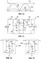
- ZC-ZVS cell 450 can be implemented either as configuration 1200 ("Type A") shown in Fig. 12, or as configuration 1300 ("Type B") shown in Fig. 13.
- terminal A connects to a current source point of the power stage (e.g. the output terminal of boost inductor 408)
- terminal C connects to the power-stage rectifier (e.g., boost rectifier 406)
- terminal B connects to the input-voltage source, or the common ground of the power stage.
- boost inductor 408 connects to the common point between boost switch 402 and snubber inductor 401.
- boost inductor 408 connects to the common point between terminal C and snubber inductor 401.
- ZC-ZVS cell 450 can be used in conjunction with other power converters.
- Figs. 14, 15, and 16 show, respectively, applications of ZC-ZVS cell 1300 in buck converter 1400, boost converter 1500, and buck-boost converter 1600.
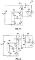
- Figs. 17, 18, 19, 20, 21 and 22 show, respectively, applications of ZC-ZVS cell 1300 in flyback converter 1700, forward converter 1800, interleaved forward converter 1900, two-switch forward converter 2000, bi-directional converter 2100, and voltage-fed full-bridge converter 2200.
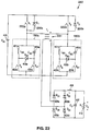
- Fig. 23 shows an application of ZC-ZVS cell 1300 in three-phase rectifier 2300.
Landscapes
- Engineering & Computer Science (AREA)
- Power Engineering (AREA)
- Dc-Dc Converters (AREA)
Abstract
Description


| Measured efficiency of the experimental boost converter input-current-shaper in the 200-W to 1-kW range at the minimum line voltage (90 VAC) and maximum line voltage (264 VAC) with and without the active snubber of the present invention: | ||||
| Power | Without active snubber | with active snubber | ||
| (W) | VIN=90VAC | VIN=264VAC | VIN=90VAC | VIN=264VAC |
| 200 | 94.2% | 97.5% | 93.2% | 96.6% |
| 300 | 93.9% | 97.8% | 93.4% | 97.1% |
| 400 | 93.6% | 98.1% | 93.3% | 97.5% |
| 500 | 93.2% | 97.8% | 93.8% | 97.5% |
| 600 | 93.0% | 98.0% | 94.4% | 97.8% |
| 700 | 92.7% | 97.9% | 94.5% | 98.5% |
| 800 | 92.0% | 97.8% | 93.8% | 98.6% |
| 900 | 90.5% | 98.1% | 93.4% | 98.5% |
| 1000 | n/a | 98.1% | 92.5% | 98.4% |
Claims (24)
- A power converter including a zero-current, zero-voltage switching (ZC-ZVS) cell, said ZC-ZVS cell having a first terminal, a second terminal and a third terminal, said ZC-ZVS cell comprising:a diode;a first switch coupled between said second terminal and an anode of said diode;a second switch coupled between said second terminal and a cathode of said diode;a capacitor coupled between said third terminal and said cathode of said diode; andan inductor coupled between said anode of said diode and said third terminal.
- A power converter as in Claim 1, wherein said anode of said diode is coupled to said first terminal.
- A power converter as in Claim 1, wherein said first and third terminals are shorted.
- A power converter as in Claim 1, further comprising a diode coupled across said first switch.
- A power converter as in Claim 1, further comprising a diode coupled across said second switch.
- A power converter as in Claim 1, further comprising a diode coupled across the terminals of said capacitor.
- A power converter as in Claim 1, further comprising a resistor coupled in across the terminals of said capacitor.
- A power converter as in Claim 1, further comprising a capacitor coupled across said second switch.
- A power converter as in Claim 1, wherein said first switch and second switch are closed over overlapping time intervals.
- A power converter as in Claim 9, wherein said overlapping time intervals, said first switch is closed prior to a closing of said second switch, and wherein said first switch is opened prior to an opening of said second switch.
- A power converter as in any one of Claims 1 to 10, wherein said first switch comprises an insulated gate bipolar transistor.
- A power converter as in any one of Claims 1 to 10, wherein said second switch comprises a field effect transistor.
- A power converter as in any one of Claims 1 to 10, wherein said first switch comprises a field effect transistor.
- A power converter as in any one of Claims 1 to 10, wherein said second switch comprises an insulated gate bipolar transistor.
- A power converter as in any one of Claims 1 to 14, wherein said power converter comprises a boost converter.
- A power converter as in any one of Claims 1 to 14, wherein said power converter comprises a buck converter.
- A power converter as in any one of Claims 1 to 14, wherein said power converter comprises a buck-boost converter.
- A power converter as in any one of Claims 1 to 14, wherein said power converter comprises a flyback converter.
- A power converter as in any one of Claims 1 to 14, wherein said power converter comprises a forward converter.
- A power converter as in any one of Claims 1 to 14, wherein said power converter comprises an interleaved forward converter.
- A power converter as in any one of Claims 1 to 14, wherein said power converter comprises a two-switch forward converter.
- A power converter as in any one of Claims 1 to 14, wherein said power converter comprises a bi-directional converter.
- A power converter as in any one of Claims 1 to 14, wherein said power converter comprises a voltage-fed full-bridge converter.
- A power converter as in any one of Claims 1 to 14, wherein said power converter comprises a three-phase rectifier.
Applications Claiming Priority (2)
| Application Number | Priority Date | Filing Date | Title |
|---|---|---|---|
| US250789 | 1999-02-11 | ||
| US09/250,789 US6051961A (en) | 1999-02-11 | 1999-02-11 | Soft-switching cell for reducing switching losses in pulse-width-modulated converters |
Publications (3)
| Publication Number | Publication Date |
|---|---|
| EP1028518A2 true EP1028518A2 (en) | 2000-08-16 |
| EP1028518A3 EP1028518A3 (en) | 2003-05-02 |
| EP1028518B1 EP1028518B1 (en) | 2005-08-03 |
Family
ID=22949154
Family Applications (1)
| Application Number | Title | Priority Date | Filing Date |
|---|---|---|---|
| EP00301054A Expired - Lifetime EP1028518B1 (en) | 1999-02-11 | 2000-02-10 | Soft-switching cell for reducing switching losses in pulse-width-modulated converters |
Country Status (5)
| Country | Link |
|---|---|
| US (1) | US6051961A (en) |
| EP (1) | EP1028518B1 (en) |
| JP (1) | JP4528404B2 (en) |
| DE (1) | DE60021637T2 (en) |
| TW (1) | TW475317B (en) |
Cited By (5)
| Publication number | Priority date | Publication date | Assignee | Title |
|---|---|---|---|---|
| KR100917169B1 (en) * | 2002-09-12 | 2009-09-15 | 페어차일드코리아반도체 주식회사 | Switching method using ITV module and ITV driver circuit for same |
| CN101222177B (en) * | 2006-12-27 | 2010-07-14 | 康舒科技股份有限公司 | voltage conversion circuit |
| CN110277905A (en) * | 2019-07-22 | 2019-09-24 | 哈尔滨理工大学 | Digital control method of power supply, power factor correction stage, and power factor correction method |
| CN113285599A (en) * | 2021-05-27 | 2021-08-20 | 潍柴动力股份有限公司 | Soft switching bidirectional direct current converter and control method |
| US11973436B2 (en) | 2017-06-12 | 2024-04-30 | Tae Technologies, Inc. | Multi-level multi-quadrant hysteresis current controllers and methods for control thereof |
Families Citing this family (77)
| Publication number | Priority date | Publication date | Assignee | Title |
|---|---|---|---|---|
| CN1055804C (en) * | 1998-04-27 | 2000-08-23 | 深圳市华为电气股份有限公司 | Topological circuit for soft switch |
| SE520419C2 (en) | 2000-03-24 | 2003-07-08 | Emerson Energy Systems Ab | Cutting circuit for zero voltage switch |
| WO2001082461A2 (en) | 2000-04-20 | 2001-11-01 | Intersil Corporation | Quasi-resonant converter |
| US6341076B1 (en) | 2000-05-23 | 2002-01-22 | Next Power Corporation | Loss reduction circuit for switching power converters |
| US6236191B1 (en) | 2000-06-02 | 2001-05-22 | Astec International Limited | Zero voltage switching boost topology |
| US6198260B1 (en) * | 2000-06-05 | 2001-03-06 | Technical Witts, Inc. | Zero voltage switching active reset power converters |
| CN1136648C (en) * | 2000-07-05 | 2004-01-28 | Tdk股份有限公司 | power conversion device |
| US6495993B2 (en) * | 2001-02-20 | 2002-12-17 | Linear Technology Corporation | Circuitry for improving the efficiency of a switching regulator by reducing reverse recovery current |
| JP3680747B2 (en) * | 2001-03-09 | 2005-08-10 | ソニー株式会社 | Switching power supply circuit |
| FR2821996B1 (en) * | 2001-03-09 | 2003-06-13 | St Microelectronics Sa | CIRCUIT FOR SWITCHING A CUT-OUT CONVERTER |
| US6452814B1 (en) * | 2001-09-19 | 2002-09-17 | Technical Witts, Inc. | Zero voltage switching cells for power converters |
| US6434029B1 (en) | 2001-10-17 | 2002-08-13 | Astec International Limited | Boost topology having an auxiliary winding on the snubber inductor |
| CN100349371C (en) * | 2001-11-22 | 2007-11-14 | 中兴通讯股份有限公司 | Control device for zero-voltage conversion step-up power factor correcting circuit |
| DE10234080A1 (en) * | 2002-07-26 | 2004-02-05 | Philips Intellectual Property & Standards Gmbh | DC buck converter |
| US6939347B2 (en) * | 2002-11-19 | 2005-09-06 | Conmed Corporation | Electrosurgical generator and method with voltage and frequency regulated high-voltage current mode power supply |
| US6809503B1 (en) | 2003-01-13 | 2004-10-26 | Linear Technology Corporation | Systems and methods for conserving energy in a switching circuit |
| US7408793B2 (en) * | 2003-02-11 | 2008-08-05 | Det International Holding Limited | Active snubber |
| TWI221053B (en) * | 2003-05-07 | 2004-09-11 | Uis Abler Electronics Co Ltd | Bi-directional dc/dc power converter with a neutral point |
| US6987675B2 (en) * | 2003-05-23 | 2006-01-17 | Delta Electronics, Inc. | Soft-switched power converters |
| JP4535492B2 (en) * | 2004-07-21 | 2010-09-01 | 株式会社京三製作所 | Buck-boost chopper circuit |
| CN100356670C (en) * | 2004-08-20 | 2007-12-19 | 艾默生网络能源有限公司 | Soft switch power factor correcting circuit |
| DE102004050060B4 (en) * | 2004-10-13 | 2018-02-08 | Osram Gmbh | Buck converter circuit |
| US20060267561A1 (en) * | 2005-05-27 | 2006-11-30 | Cherokee International Corporation | Power factor correction circuit for DC-DC converters with low resonance current |
| GB0526635D0 (en) * | 2005-12-30 | 2006-02-08 | Microgen Energy Ltd | Switching controller |
| GB0526625D0 (en) * | 2005-12-30 | 2006-02-08 | Microgen Energy Ltd | Power supply |
| US7609037B1 (en) * | 2006-06-23 | 2009-10-27 | Edward Herbert | “Natural modulation” for maximizing efficiency in power converters |
| TWI319652B (en) | 2006-07-26 | 2010-01-11 | Benq Corp | Low acoustic noise solution for snubber circuit |
| US7579814B2 (en) * | 2007-01-12 | 2009-08-25 | Potentia Semiconductor Corporation | Power converter with snubber |
| FR2929054B1 (en) * | 2008-03-21 | 2014-06-20 | Commissariat Energie Atomique | DECOUPAGE POWER SUPPLY DC DC NOT ISOLATED |
| US7915879B2 (en) * | 2008-06-30 | 2011-03-29 | Infineon Technologies Austria Ag | Switching converter including a rectifier element with nonlinear capacitance |
| US8659273B2 (en) * | 2008-10-27 | 2014-02-25 | Dell Products L.P. | Soft-switching voltage regulation in a step-down circuit |
| JP5523811B2 (en) * | 2009-12-16 | 2014-06-18 | 川崎重工業株式会社 | Soft switching step-down chopper and power supply system |
| US8148853B2 (en) * | 2009-12-30 | 2012-04-03 | American Power Conversion Corporation | Switching method and apparatus |
| JP5342021B2 (en) * | 2010-01-05 | 2013-11-13 | 株式会社日立製作所 | AC-DC converter and control method thereof |
| US8436593B2 (en) | 2010-02-15 | 2013-05-07 | Stmicroelectronics, Inc. | Wide input voltage range power factor correction circuit |
| US8829865B2 (en) * | 2010-07-13 | 2014-09-09 | General Electric Company | Power factor correction efficiency improvement circuit, a converter employing the circuit and a method of manufacturing a converter |
| US8773085B2 (en) | 2011-03-22 | 2014-07-08 | Ledillion Technologies Inc. | Apparatus and method for efficient DC-to-DC conversion through wide voltage swings |
| TWI455464B (en) * | 2011-05-10 | 2014-10-01 | Jiann Fuh Chen | Dc-dc voltage booster circuit and control method thereof |
| JP2013169057A (en) * | 2012-02-15 | 2013-08-29 | Sanken Electric Co Ltd | Switching power-supply circuit |
| TWI452811B (en) * | 2012-03-01 | 2014-09-11 | Nat Univ Tsing Hua | Single - stage single - switch power conversion device |
| DE102012204255A1 (en) * | 2012-03-19 | 2013-09-19 | Siemens Aktiengesellschaft | DC converter |
| KR101376844B1 (en) * | 2012-12-11 | 2014-04-01 | 삼성전기주식회사 | Power factor correction circuit and power supply having the same |
| CN103151916A (en) * | 2013-03-22 | 2013-06-12 | 深圳市航天新源科技有限公司 | Low-ripple two-way soft switch DC-DC (direct current to direct current) circuit and uninterruptible power supply |
| WO2015079538A1 (en) * | 2013-11-28 | 2015-06-04 | 株式会社安川電機 | Dc-dc converter |
| KR101630076B1 (en) * | 2014-11-07 | 2016-06-13 | 삼성전기주식회사 | Power factor corection apparatus and power supplying apparatus having the same and motor driving apparatus having the same |
| US9582016B2 (en) * | 2015-02-05 | 2017-02-28 | Silicon Laboratories Inc. | Boost converter with capacitive boost stages |
| CN104734302B (en) * | 2015-04-09 | 2017-03-15 | 北京京东方能源科技有限公司 | Power-supplying circuit and method of supplying power to |
| TWI560987B (en) * | 2015-07-13 | 2016-12-01 | Univ Kun Shan | Direct current power converter |
| EP3358733A4 (en) * | 2015-12-04 | 2019-04-17 | Murata Manufacturing Co., Ltd. | POWER CONVERSION DEVICE |
| US10193442B2 (en) | 2016-02-09 | 2019-01-29 | Faraday Semi, LLC | Chip embedded power converters |
| US20180323713A1 (en) | 2017-04-18 | 2018-11-08 | EMD Technologies Incorporated | Soft-switching for high-frequency power conversion |
| WO2018232403A1 (en) | 2017-06-16 | 2018-12-20 | Tae Technologies, Inc. | Multi-level hysteresis voltage controllers for voltage modulators and methods for control thereof |
| CN107659141A (en) * | 2017-11-01 | 2018-02-02 | 广东工业大学 | A kind of converter circuit |
| SG11202009200TA (en) | 2018-03-22 | 2020-10-29 | Tae Technologies Inc | Systems and methods for power management and control |
| CN109120142A (en) * | 2018-11-05 | 2019-01-01 | 宁波市北仑临宇电子科技有限公司 | The lossless synchronous absorbing circuit of peak voltage, boosting and step-down switching power supply circuit |
| US10504848B1 (en) | 2019-02-19 | 2019-12-10 | Faraday Semi, Inc. | Chip embedded integrated voltage regulator |
| AU2020253330B2 (en) | 2019-03-29 | 2025-10-02 | Tae Technologies, Inc. | Module-based energy systems capable of cascaded and interconnected configurations, and methods related thereto |
| WO2020214857A1 (en) | 2019-04-17 | 2020-10-22 | Faraday Semi, Inc. | Electrical devices and methods of manufacture |
| AU2020282353A1 (en) | 2019-05-30 | 2021-12-16 | Tae Technologies, Inc. | Advanced battery charging on modular levels of energy storage systems |
| CN110120749B (en) * | 2019-06-13 | 2024-08-13 | 深圳线易微电子有限公司 | Power converter and chip |
| TWI716110B (en) * | 2019-09-20 | 2021-01-11 | 崑山科技大學 | Soft-switching interleaved active clamp high step-up dc converter |
| US11897347B2 (en) | 2020-04-14 | 2024-02-13 | Tae Technologies, Inc. | Systems, devices, and methods for charging and discharging module-based cascaded energy systems |
| WO2021211635A1 (en) | 2020-04-14 | 2021-10-21 | Tae Technologies, Inc. | Modular cascaded energy systems with a cooling apparatus and with replaceable energy source capability |
| CA3179327A1 (en) | 2020-05-14 | 2021-11-18 | Tae Technologies, Inc. | Systems, devices, and methods for rail-based and other electric vehicles with modular cascaded energy systems |
| WO2021235561A1 (en) * | 2020-05-18 | 2021-11-25 | 엘지마그나 이파워트레인 주식회사 | Inverter device |
| CN111697957B (en) * | 2020-06-17 | 2024-03-12 | 上海电气集团股份有限公司 | Driving circuit applied to insulated gate bipolar transistor IGBT |
| US11063516B1 (en) | 2020-07-29 | 2021-07-13 | Faraday Semi, Inc. | Power converters with bootstrap |
| US20240359595A1 (en) * | 2020-08-24 | 2024-10-31 | Tae Technologies, Inc. | Modular Cascaded Energy Systems with a Cooling Apparatus and with Replaceable Energy Source Capability |
| CA3196955A1 (en) | 2020-09-28 | 2022-03-31 | Tae Technologies, Inc. | Multi-phase module-based energy system frameworks and methods related thereto |
| CN116235402B (en) * | 2020-09-30 | 2024-06-04 | 大金工业株式会社 | Power conversion device |
| US20220097559A1 (en) | 2020-09-30 | 2022-03-31 | Tae Technologies, Inc. | Systems, devices, and methods for intraphase and interphase balancing in module-based cascaded energy systems |
| WO2022155266A1 (en) | 2021-01-13 | 2022-07-21 | Tae Technologies, Inc. | Systems, devices, and methods for module-based cascaded energy systems |
| TWI767852B (en) * | 2021-04-01 | 2022-06-11 | 立錡科技股份有限公司 | Switching regulator achieveing soft switching by double switching and control circuit thereof |
| US11601036B2 (en) | 2021-04-16 | 2023-03-07 | Delta Electronics, Inc. | AC-DC power conversion system with zero voltage switching |
| WO2023283260A1 (en) | 2021-07-07 | 2023-01-12 | Tae Technologies, Inc. | Systems, devices, and methods for module-based cascaded energy systems configured to interface with renewable energy sources |
| US11990839B2 (en) | 2022-06-21 | 2024-05-21 | Faraday Semi, Inc. | Power converters with large duty cycles |
| CN118174555A (en) * | 2022-12-09 | 2024-06-11 | 台达电子企业管理(上海)有限公司 | Switching power converter and control method thereof |
Family Cites Families (10)
| Publication number | Priority date | Publication date | Assignee | Title |
|---|---|---|---|---|
| US3467852A (en) * | 1967-01-26 | 1969-09-16 | Trw Inc | High speed controlled switching circuit |
| US5146399A (en) * | 1989-08-14 | 1992-09-08 | Jeff Gucyski | Switching power apparatus having high factor and comprising pair of converter for obtaining fixed or variable output voltage |
| CH682611A5 (en) * | 1991-04-16 | 1993-10-15 | Hasler Ag Ascom | Snubber for switch-regulated energy boost converter - uses switched discharge coil across energy converter switch operated by offset overlapping switch signal |
| US5418704A (en) * | 1992-06-12 | 1995-05-23 | Center For Innovative Technology | Zero-voltage-transition pulse-width-modulated converters |
| US5313382A (en) * | 1993-05-18 | 1994-05-17 | At&T Bell Laboratories | Reduced voltage/zero current transition boost power converter |
| US5446366A (en) * | 1994-02-08 | 1995-08-29 | Computer Products, Inc. | Boost converter power supply with reduced losses, control circuit and method therefor |
| JPH0951260A (en) * | 1995-05-26 | 1997-02-18 | Murata Mfg Co Ltd | Fet drive circuit |
| US5736842A (en) * | 1996-07-11 | 1998-04-07 | Delta Electronics, Inc. | Technique for reducing rectifier reverse-recovery-related losses in high-voltage high power converters |
| US5815386A (en) * | 1997-06-19 | 1998-09-29 | Factor One, Inc. | Snubber for zero current switched networks |
| US5914587A (en) * | 1997-08-05 | 1999-06-22 | Lucent Technologies Inc. | Circuit for reducing switching losses of a power converter and method of operation thereof |
-
1999
- 1999-02-11 US US09/250,789 patent/US6051961A/en not_active Expired - Lifetime
-
2000
- 2000-02-07 JP JP2000028505A patent/JP4528404B2/en not_active Expired - Lifetime
- 2000-02-10 DE DE60021637T patent/DE60021637T2/en not_active Expired - Lifetime
- 2000-02-10 EP EP00301054A patent/EP1028518B1/en not_active Expired - Lifetime
- 2000-03-27 TW TW089102202A patent/TW475317B/en not_active IP Right Cessation
Cited By (6)
| Publication number | Priority date | Publication date | Assignee | Title |
|---|---|---|---|---|
| KR100917169B1 (en) * | 2002-09-12 | 2009-09-15 | 페어차일드코리아반도체 주식회사 | Switching method using ITV module and ITV driver circuit for same |
| CN101222177B (en) * | 2006-12-27 | 2010-07-14 | 康舒科技股份有限公司 | voltage conversion circuit |
| US11973436B2 (en) | 2017-06-12 | 2024-04-30 | Tae Technologies, Inc. | Multi-level multi-quadrant hysteresis current controllers and methods for control thereof |
| CN110277905A (en) * | 2019-07-22 | 2019-09-24 | 哈尔滨理工大学 | Digital control method of power supply, power factor correction stage, and power factor correction method |
| CN113285599A (en) * | 2021-05-27 | 2021-08-20 | 潍柴动力股份有限公司 | Soft switching bidirectional direct current converter and control method |
| CN113285599B (en) * | 2021-05-27 | 2022-04-26 | 潍柴动力股份有限公司 | Soft switching bidirectional direct current converter and control method |
Also Published As
| Publication number | Publication date |
|---|---|
| JP4528404B2 (en) | 2010-08-18 |
| DE60021637T2 (en) | 2006-05-24 |
| EP1028518B1 (en) | 2005-08-03 |
| US6051961A (en) | 2000-04-18 |
| EP1028518A3 (en) | 2003-05-02 |
| DE60021637D1 (en) | 2005-09-08 |
| TW475317B (en) | 2002-02-01 |
| JP2000232775A (en) | 2000-08-22 |
Similar Documents
| Publication | Publication Date | Title |
|---|---|---|
| EP1028518B1 (en) | Soft-switching cell for reducing switching losses in pulse-width-modulated converters | |
| US5959438A (en) | Soft-switched boost converter with isolated active snubber | |
| US6028418A (en) | Boost converter with minimum-component-count active snubber | |
| US5736842A (en) | Technique for reducing rectifier reverse-recovery-related losses in high-voltage high power converters | |
| US6525513B1 (en) | Soft switching topological circuit in boost or buck converter | |
| US5313382A (en) | Reduced voltage/zero current transition boost power converter | |
| US5636114A (en) | Lossless snubber circuit for use in power converters | |
| US5287261A (en) | Power conversion using zero current soft switching | |
| Jovanovic et al. | State-of-the-art, single-phase, active power-factor-correction techniques for high-power applications-an overview | |
| US6069803A (en) | Offset resonance zero volt switching flyback converter | |
| US7218081B2 (en) | Power system having multiple power converters with reduced switching loss | |
| US7518895B2 (en) | High-efficiency power converter system | |
| US6987675B2 (en) | Soft-switched power converters | |
| US8085083B2 (en) | Current-source gate driver | |
| Das et al. | A comparative study of zero-current-transition PWM converters | |
| EP2713488B1 (en) | Electronic converter, and related lighting system and method of operating an electronic converter | |
| US4953068A (en) | Full bridge power converter with multiple zero voltage resonant transition switching | |
| Oruganti et al. | Soft-switched DC/DC converter with PWM control | |
| EP1243065B1 (en) | Resonant gate drive for synchronous rectifiers | |
| US7233507B2 (en) | Non dissipative snubber circuit with saturable reactor | |
| US6341076B1 (en) | Loss reduction circuit for switching power converters | |
| US5982638A (en) | Single stage power converter with regenerative snubber and power factor correction | |
| Gurunathan et al. | A zero-voltage transition boost converter using a zero-voltage switching auxiliary circuit | |
| EP3393027A1 (en) | Soft-switching for high-frequency power conversion | |
| Jovanovic | A technique for reducing rectifier reverse-recovery-related losses in high-voltage, high-power boost converters |
Legal Events
| Date | Code | Title | Description |
|---|---|---|---|
| PUAI | Public reference made under article 153(3) epc to a published international application that has entered the european phase |
Free format text: ORIGINAL CODE: 0009012 |
|
| AK | Designated contracting states |
Kind code of ref document: A2 Designated state(s): AT BE CH CY DE DK ES FI FR GB GR IE IT LI LU MC NL PT SE |
|
| AX | Request for extension of the european patent |
Free format text: AL;LT;LV;MK;RO;SI |
|
| 17P | Request for examination filed |
Effective date: 20001009 |
|
| PUAL | Search report despatched |
Free format text: ORIGINAL CODE: 0009013 |
|
| AK | Designated contracting states |
Designated state(s): DE ES FR GB IT SE |
|
| AX | Request for extension of the european patent |
Extension state: AL LT LV MK RO SI |
|
| AKX | Designation fees paid |
Designated state(s): DE ES FR GB IT SE |
|
| 17Q | First examination report despatched |
Effective date: 20040216 |
|
| GRAP | Despatch of communication of intention to grant a patent |
Free format text: ORIGINAL CODE: EPIDOSNIGR1 |
|
| GRAS | Grant fee paid |
Free format text: ORIGINAL CODE: EPIDOSNIGR3 |
|
| GRAA | (expected) grant |
Free format text: ORIGINAL CODE: 0009210 |
|
| AK | Designated contracting states |
Kind code of ref document: B1 Designated state(s): DE ES FR GB IT SE |
|
| PG25 | Lapsed in a contracting state [announced via postgrant information from national office to epo] |
Ref country code: IT Free format text: LAPSE BECAUSE OF FAILURE TO SUBMIT A TRANSLATION OF THE DESCRIPTION OR TO PAY THE FEE WITHIN THE PRESCRIBED TIME-LIMIT;WARNING: LAPSES OF ITALIAN PATENTS WITH EFFECTIVE DATE BEFORE 2007 MAY HAVE OCCURRED AT ANY TIME BEFORE 2007. THE CORRECT EFFECTIVE DATE MAY BE DIFFERENT FROM THE ONE RECORDED. Effective date: 20050803 |
|
| REG | Reference to a national code |
Ref country code: GB Ref legal event code: FG4D |
|
| REF | Corresponds to: |
Ref document number: 60021637 Country of ref document: DE Date of ref document: 20050908 Kind code of ref document: P |
|
| PG25 | Lapsed in a contracting state [announced via postgrant information from national office to epo] |
Ref country code: SE Free format text: LAPSE BECAUSE OF FAILURE TO SUBMIT A TRANSLATION OF THE DESCRIPTION OR TO PAY THE FEE WITHIN THE PRESCRIBED TIME-LIMIT Effective date: 20051103 |
|
| PG25 | Lapsed in a contracting state [announced via postgrant information from national office to epo] |
Ref country code: ES Free format text: LAPSE BECAUSE OF FAILURE TO SUBMIT A TRANSLATION OF THE DESCRIPTION OR TO PAY THE FEE WITHIN THE PRESCRIBED TIME-LIMIT Effective date: 20051114 |
|
| PLBE | No opposition filed within time limit |
Free format text: ORIGINAL CODE: 0009261 |
|
| STAA | Information on the status of an ep patent application or granted ep patent |
Free format text: STATUS: NO OPPOSITION FILED WITHIN TIME LIMIT |
|
| 26N | No opposition filed |
Effective date: 20060504 |
|
| EN | Fr: translation not filed | ||
| PG25 | Lapsed in a contracting state [announced via postgrant information from national office to epo] |
Ref country code: FR Free format text: LAPSE BECAUSE OF FAILURE TO SUBMIT A TRANSLATION OF THE DESCRIPTION OR TO PAY THE FEE WITHIN THE PRESCRIBED TIME-LIMIT Effective date: 20060929 |
|
| PG25 | Lapsed in a contracting state [announced via postgrant information from national office to epo] |
Ref country code: FR Free format text: LAPSE BECAUSE OF FAILURE TO SUBMIT A TRANSLATION OF THE DESCRIPTION OR TO PAY THE FEE WITHIN THE PRESCRIBED TIME-LIMIT Effective date: 20050803 |
|
| PGFP | Annual fee paid to national office [announced via postgrant information from national office to epo] |
Ref country code: DE Payment date: 20190227 Year of fee payment: 20 Ref country code: GB Payment date: 20190227 Year of fee payment: 20 |
|
| REG | Reference to a national code |
Ref country code: DE Ref legal event code: R071 Ref document number: 60021637 Country of ref document: DE |
|
| REG | Reference to a national code |
Ref country code: GB Ref legal event code: PE20 Expiry date: 20200209 |
|
| PG25 | Lapsed in a contracting state [announced via postgrant information from national office to epo] |
Ref country code: GB Free format text: LAPSE BECAUSE OF EXPIRATION OF PROTECTION Effective date: 20200209 |