JP2013169057A - Switching power-supply circuit - Google Patents
Switching power-supply circuit Download PDFInfo
- Publication number
- JP2013169057A JP2013169057A JP2012030361A JP2012030361A JP2013169057A JP 2013169057 A JP2013169057 A JP 2013169057A JP 2012030361 A JP2012030361 A JP 2012030361A JP 2012030361 A JP2012030361 A JP 2012030361A JP 2013169057 A JP2013169057 A JP 2013169057A
- Authority
- JP
- Japan
- Prior art keywords
- diode
- power supply
- switching
- supply circuit
- switching element
- Prior art date
- Legal status (The legal status is an assumption and is not a legal conclusion. Google has not performed a legal analysis and makes no representation as to the accuracy of the status listed.)
- Pending
Links
Images


Classifications
-
- G—PHYSICS
- G05—CONTROLLING; REGULATING
- G05F—SYSTEMS FOR REGULATING ELECTRIC OR MAGNETIC VARIABLES
- G05F1/00—Automatic systems in which deviations of an electric quantity from one or more predetermined values are detected at the output of the system and fed back to a device within the system to restore the detected quantity to its predetermined value or values, i.e. retroactive systems
- G05F1/10—Regulating voltage or current
- G05F1/46—Regulating voltage or current wherein the variable actually regulated by the final control device is dc
- G05F1/468—Regulating voltage or current wherein the variable actually regulated by the final control device is dc characterised by reference voltage circuitry, e.g. soft start, remote shutdown
-
- H—ELECTRICITY
- H02—GENERATION; CONVERSION OR DISTRIBUTION OF ELECTRIC POWER
- H02M—APPARATUS FOR CONVERSION BETWEEN AC AND AC, BETWEEN AC AND DC, OR BETWEEN DC AND DC, AND FOR USE WITH MAINS OR SIMILAR POWER SUPPLY SYSTEMS; CONVERSION OF DC OR AC INPUT POWER INTO SURGE OUTPUT POWER; CONTROL OR REGULATION THEREOF
- H02M1/00—Details of apparatus for conversion
- H02M1/32—Means for protecting converters other than automatic disconnection
- H02M1/34—Snubber circuits
-
- H—ELECTRICITY
- H02—GENERATION; CONVERSION OR DISTRIBUTION OF ELECTRIC POWER
- H02M—APPARATUS FOR CONVERSION BETWEEN AC AND AC, BETWEEN AC AND DC, OR BETWEEN DC AND DC, AND FOR USE WITH MAINS OR SIMILAR POWER SUPPLY SYSTEMS; CONVERSION OF DC OR AC INPUT POWER INTO SURGE OUTPUT POWER; CONTROL OR REGULATION THEREOF
- H02M3/00—Conversion of dc power input into dc power output
- H02M3/02—Conversion of dc power input into dc power output without intermediate conversion into ac
- H02M3/04—Conversion of dc power input into dc power output without intermediate conversion into ac by static converters
- H02M3/10—Conversion of dc power input into dc power output without intermediate conversion into ac by static converters using discharge tubes with control electrode or semiconductor devices with control electrode
- H02M3/145—Conversion of dc power input into dc power output without intermediate conversion into ac by static converters using discharge tubes with control electrode or semiconductor devices with control electrode using devices of a triode or transistor type requiring continuous application of a control signal
- H02M3/155—Conversion of dc power input into dc power output without intermediate conversion into ac by static converters using discharge tubes with control electrode or semiconductor devices with control electrode using devices of a triode or transistor type requiring continuous application of a control signal using semiconductor devices only
- H02M3/156—Conversion of dc power input into dc power output without intermediate conversion into ac by static converters using discharge tubes with control electrode or semiconductor devices with control electrode using devices of a triode or transistor type requiring continuous application of a control signal using semiconductor devices only with automatic control of output voltage or current, e.g. switching regulators
- H02M3/158—Conversion of dc power input into dc power output without intermediate conversion into ac by static converters using discharge tubes with control electrode or semiconductor devices with control electrode using devices of a triode or transistor type requiring continuous application of a control signal using semiconductor devices only with automatic control of output voltage or current, e.g. switching regulators including plural semiconductor devices as final control devices for a single load
-
- H—ELECTRICITY
- H02—GENERATION; CONVERSION OR DISTRIBUTION OF ELECTRIC POWER
- H02M—APPARATUS FOR CONVERSION BETWEEN AC AND AC, BETWEEN AC AND DC, OR BETWEEN DC AND DC, AND FOR USE WITH MAINS OR SIMILAR POWER SUPPLY SYSTEMS; CONVERSION OF DC OR AC INPUT POWER INTO SURGE OUTPUT POWER; CONTROL OR REGULATION THEREOF
- H02M1/00—Details of apparatus for conversion
- H02M1/32—Means for protecting converters other than automatic disconnection
- H02M1/34—Snubber circuits
- H02M1/342—Active non-dissipative snubbers
-
- Y—GENERAL TAGGING OF NEW TECHNOLOGICAL DEVELOPMENTS; GENERAL TAGGING OF CROSS-SECTIONAL TECHNOLOGIES SPANNING OVER SEVERAL SECTIONS OF THE IPC; TECHNICAL SUBJECTS COVERED BY FORMER USPC CROSS-REFERENCE ART COLLECTIONS [XRACs] AND DIGESTS
- Y02—TECHNOLOGIES OR APPLICATIONS FOR MITIGATION OR ADAPTATION AGAINST CLIMATE CHANGE
- Y02B—CLIMATE CHANGE MITIGATION TECHNOLOGIES RELATED TO BUILDINGS, e.g. HOUSING, HOUSE APPLIANCES OR RELATED END-USER APPLICATIONS
- Y02B70/00—Technologies for an efficient end-user side electric power management and consumption
- Y02B70/10—Technologies improving the efficiency by using switched-mode power supplies [SMPS], i.e. efficient power electronics conversion e.g. power factor correction or reduction of losses in power supplies or efficient standby modes
Abstract
Description
本発明は、スイッチング損失を低減できるスイッチング電源回路に関する。 The present invention relates to a switching power supply circuit that can reduce switching loss.
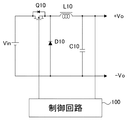
従来、降圧型のスイッチング電源回路が知られている。図6に従来の降圧型のスイッチング電源回路の一例を示す。図6において、直流電源Vinの両端には、スイッチング素子Q10とリアクトルL10と平滑コンデンサC10との直列回路が接続されている。また、スイッチング素子Q10とリアクトルL10との接続点と直流電源Vinの負極端とには、還流用ダイオードとしてダイオードD10が接続されている。 Conventionally, a step-down switching power supply circuit is known. FIG. 6 shows an example of a conventional step-down switching power supply circuit. In FIG. 6, a series circuit of a switching element Q10, a reactor L10, and a smoothing capacitor C10 is connected to both ends of the DC power supply Vin. In addition, a diode D10 is connected as a reflux diode to the connection point between the switching element Q10 and the reactor L10 and the negative terminal of the DC power supply Vin.
制御回路100は、平滑コンデンサC10から出力電圧Voを検出して、出力電圧Voが直流電源Vinの電圧(入力電圧)よりも低い所定値となるようにスイッチング素子Q10のオン・オフを制御する。
The
次に、図6に示す従来の降圧型のスイッチング電源回路の動作を説明する。まず、スイッチング素子Q10がオンすると、Vin→Q10→L10→C10→Vinの経路に電流が流れる。また、ダイオードD10には、直流電源Vinの電圧が逆方向電圧として印加される。次いで、スイッチング素子Q10がオフすると、L10→C10→D10→L10の経路に電流(還流電流)が流れる。この電流は、ダイオードD10に対して順方向に流れる。 Next, the operation of the conventional step-down switching power supply circuit shown in FIG. 6 will be described. First, when the switching element Q10 is turned on, a current flows through a path of Vin → Q10 → L10 → C10 → Vin. Further, the voltage of the DC power source Vin is applied to the diode D10 as a reverse voltage. Next, when the switching element Q10 is turned off, a current (reflux current) flows through a path of L10 → C10 → D10 → L10. This current flows in the forward direction with respect to the diode D10.
なお、従来の技術の関連技術として、例えば特許文献1に記載された還流ダイオードの逆回復電流を防止した二相DC/DCコンバータが知られている。
As a related art of the prior art, for example, a two-phase DC / DC converter that prevents reverse recovery current of a freewheeling diode described in
しかしながら、この種の従来の降圧型のスイッチング電源回路では、ダイオードD10に順方向電流が流れている時に、再び、スイッチング素子Q10がオンすると、ダイオードD10には、直流電源Vinの電圧が逆方向電圧として印加されるので、大きな逆回復電流が流れる。この逆回復電流はスイッチング素子Q10にも流れる。このため、スイッチング素子Q10、ダイオードD10でスイッチング損失が発生し、ノイズも大きくなるという問題があった。 However, in this type of conventional step-down switching power supply circuit, when the forward current flows in the diode D10, the switching element Q10 is turned on again, and the voltage of the DC power supply Vin is applied to the diode D10. As a result, a large reverse recovery current flows. This reverse recovery current also flows through switching element Q10. For this reason, there is a problem in that switching loss occurs in the switching element Q10 and the diode D10, and noise increases.
そこで、本発明は、スイッチング損失を低減できるスイッチング電源回路を提供することを目的とする。 Accordingly, an object of the present invention is to provide a switching power supply circuit that can reduce switching loss.
本発明のスイッチング電源回路は、互いに磁気的に結合され且つ互いの一端同士が接続された、主巻線と漏れインダクタンスを有する補助巻線とを有するリアクトルと、直流電源に主スイッチを介して並列に接続された、補助スイッチと共振コンデンサとが直列に接続された第1直列回路と、前記第1直列回路に前記補助巻線を介して並列に接続された第1ダイオードと、前記第1直列回路又は前記第1ダイオードに前記主巻線を介して並列に接続された平滑コンデンサと、前記主スイッチと前記補助スイッチとを交互にオン・オフさせて前記平滑コンデンサの出力電圧を所定値に制御する制御回路と、を有することを特徴とする。
また、本発明のスイッチング電源回路は、互いに磁気的に結合され且つ互いの一端同士が接続された、主巻線と補助巻線とを有する第1リアクトルと、前記補助巻線に直列に接続された第2リアクトルと、直流電源に主スイッチを介して並列に接続された、補助スイッチと共振コンデンサとが直列に接続された第1直列回路と、前記第1直列回路に前記補助巻線及び前記第2リアクトルを介して並列に接続された第1ダイオードと、前記第1直列回路又は前記第1ダイオードに前記主巻線を介して並列に接続された平滑コンデンサと、前記主スイッチと前記補助スイッチとを交互にオン・オフさせて前記平滑コンデンサの出力電圧を所定値に制御する制御回路と、を有することを特徴とする。
A switching power supply circuit according to the present invention includes a reactor having a main winding and an auxiliary winding having a leakage inductance that are magnetically coupled to each other and connected to each other, and a DC power supply in parallel via a main switch. A first series circuit in which an auxiliary switch and a resonant capacitor are connected in series, a first diode connected in parallel to the first series circuit via the auxiliary winding, and the first series A smoothing capacitor connected in parallel to the circuit or the first diode via the main winding, and the main switch and the auxiliary switch are alternately turned on and off to control the output voltage of the smoothing capacitor to a predetermined value. And a control circuit.
The switching power supply circuit according to the present invention includes a first reactor having a main winding and an auxiliary winding, which are magnetically coupled to each other and connected to each other, and connected in series to the auxiliary winding. A second reactor, a first series circuit in which an auxiliary switch and a resonant capacitor are connected in series to a DC power supply via a main switch, and the auxiliary winding and the first series circuit are connected to the first series circuit. A first diode connected in parallel via a second reactor; a smoothing capacitor connected in parallel to the first series circuit or the first diode via the main winding; the main switch and the auxiliary switch And a control circuit for controlling the output voltage of the smoothing capacitor to a predetermined value by alternately turning on and off.
本発明によれば、スイッチング損失を低減できるスイッチング電源回路を提供することができる。 ADVANTAGE OF THE INVENTION According to this invention, the switching power supply circuit which can reduce switching loss can be provided.
以下、本発明の実施の形態に係るスイッチング電源回路を図面に基づいて説明する。 Hereinafter, a switching power supply circuit according to an embodiment of the present invention will be described with reference to the drawings.
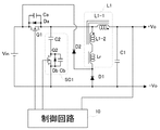
図1は、本発明の実施例1に係るスイッチング電源回路を示す図である。図1に示すスイッチング電源回路は、直流電源Vinの電圧(入力電圧)よりも低い所定値の出力電圧Voを出力する降圧型のスイッチング電源回路であり、リアクトルL1、スイッチング素子Q1、スイッチング素子Q2、平滑コンデンサC1、共振コンデンサC2、ダイオードD1(第1ダイオード)、ダイオードD2(第2ダイオード)、制御回路10を有して構成されている。
1 is a diagram illustrating a switching power supply circuit according to a first embodiment of the present invention. The switching power supply circuit shown in FIG. 1 is a step-down switching power supply circuit that outputs an output voltage Vo having a predetermined value lower than the voltage (input voltage) of the DC power supply Vin, and includes a reactor L1, a switching element Q1, a switching element Q2, The circuit includes a smoothing capacitor C1, a resonant capacitor C2, a diode D1 (first diode), a diode D2 (second diode), and a
リアクトルL1は、互いに磁気的に結合され且つ互いの一端同士が接続された、主巻線L1−1と漏れインダクタンスLrを有する補助巻線L1−2とを有する。漏れインダクタンスLrは、リアクトルL1の主巻線L1−1と補助巻線L1−2とを互いに疎結合に巻回することにより、補助巻線L1−2に等価的に直列接続されるように生成される。 Reactor L1 includes a main winding L1-1 and an auxiliary winding L1-2 having a leakage inductance Lr that are magnetically coupled to each other and connected to each other. The leakage inductance Lr is generated so as to be equivalently connected in series to the auxiliary winding L1-2 by winding the main winding L1-1 and the auxiliary winding L1-2 of the reactor L1 in a loosely coupled manner. Is done.
直流電源Vinの両端には、スイッチング素子Q1(電界効果トランジスタ)を介してスイッチング素子Q2(電界効果トランジスタ)と共振コンデンサC2とが直列に接続された第1直列回路SC1が接続されている。 Connected to both ends of the DC power supply Vin is a first series circuit SC1 in which a switching element Q2 (field effect transistor) and a resonant capacitor C2 are connected in series via a switching element Q1 (field effect transistor).
スイッチング素子Q1のドレイン−ソース間には、ダイオードDa及びコンデンサCaが接続されている。ダイオードDaはスイッチング素子Q1の寄生ダイオードでも良く、コンデンサCaはスイッチング素子Q1の寄生コンデンサでも良い。また、スイッチング素子Q2のドレイン−ソース間には、ダイオードDb及びコンデンサCbが接続されている。ダイオードDbはスイッチング素子Q2の寄生ダイオードでも良く、コンデンサCbはスイッチング素子Q2の寄生コンデンサでも良い。スイッチング素子Q1及びダイオードDaは本発明の主スイッチに対応し、スイッチング素子Q2及びダイオードDbは本発明の補助スイッチに対応する。 A diode Da and a capacitor Ca are connected between the drain and source of the switching element Q1. The diode Da may be a parasitic diode of the switching element Q1, and the capacitor Ca may be a parasitic capacitor of the switching element Q1. A diode Db and a capacitor Cb are connected between the drain and source of the switching element Q2. The diode Db may be a parasitic diode of the switching element Q2, and the capacitor Cb may be a parasitic capacitor of the switching element Q2. The switching element Q1 and the diode Da correspond to the main switch of the present invention, and the switching element Q2 and the diode Db correspond to the auxiliary switch of the present invention.
第1直列回路SC1の両端には、補助巻線L1−2及び漏れインダクタンスLrを介してダイオードD1が接続されていると共に、主巻線L1−1を介して平滑コンデンサC1が接続されている。 A diode D1 is connected to both ends of the first series circuit SC1 via an auxiliary winding L1-2 and a leakage inductance Lr, and a smoothing capacitor C1 is connected via a main winding L1-1.
また、直流電源Vinの両端には、ダイオードD1を介してダイオードD2が接続されている。ダイオードD1は還流用ダイオードであり、ダイオードD2は、ダイオードD1のカソード電位を、直流電源Vinの正極端の電位にクランプするためのクランプ用ダイオードである。 A diode D2 is connected to both ends of the DC power supply Vin via a diode D1. The diode D1 is a freewheeling diode, and the diode D2 is a clamping diode for clamping the cathode potential of the diode D1 to the potential of the positive terminal of the DC power supply Vin.
制御回路10は、平滑コンデンサC1から出力電圧Voを検出して、出力電圧Voが直流電源Vinの電圧(入力電圧)よりも低い所定値となるように、且つスイッチング素子Q1,Q2のオンがゼロ電圧スイッチング(スイッチング素子Q1,Q2のドレイン−ソース間電圧がほぼゼロである時にスイッチングすること)となるようにスイッチング素子Q1のゲート信号Q1g及びスイッチング素子Q2のゲート信号Q2gを生成する。スイッチング素子Q1,Q2は、制御回路10からのゲート信号Q1g,Q2gにより、共にオフとなる期間(デッドタイムtd)を有して交互にオン・オフされる。
The
次に、このように構成された実施例1に係るスイッチング電源回路の動作について、図2に示す波形図(タイミングチャート)を参照しながら説明する。 Next, the operation of the switching power supply circuit according to the first embodiment configured as described above will be described with reference to the waveform diagram (timing chart) shown in FIG.
図2において、Q1gはスイッチング素子Q1のゲートに印加されるゲート信号、Q2gはスイッチング素子Q2のゲートに印加されるゲート信号、Q1vはスイッチング素子Q1のドレイン−ソース間電圧、Q1iはスイッチング素子Q1のドレイン−ソース間電流、Q2vはスイッチング素子Q2のドレイン−ソース間電圧、Q2iはスイッチング素子Q2のドレイン−ソース間電流、C2vは共振コンデンサC2の両端子間電圧、D1iはダイオードD1に流れる電流、L1−1iはリアクトルL1の主巻線L1−1に流れる電流を示している。なお、C2vの基準電位点は、共振コンデンサC2のスイッチング素子Q2に接続されない方の端子である。 2, Q1g is a gate signal applied to the gate of the switching element Q1, Q2g is a gate signal applied to the gate of the switching element Q2, Q1v is a drain-source voltage of the switching element Q1, and Q1i is a voltage of the switching element Q1. The drain-source current, Q2v is the drain-source voltage of the switching element Q2, Q2i is the drain-source current of the switching element Q2, C2v is the voltage between both terminals of the resonant capacitor C2, D1i is the current flowing through the diode D1, and L1 −1i indicates a current flowing through the main winding L1-1 of the reactor L1. Note that the reference potential point of C2v is a terminal that is not connected to the switching element Q2 of the resonance capacitor C2.
まず、期間T3において、スイッチング素子Q1のオン期間にリアクトルL1に蓄えられたエネルギーが主巻線L1−1及び補助巻線L1−2に放出されて、L1−1→C1→Vin→Q1(Ca)→L1−1の第1経路と、L1−1→C1→Q2(Cb)→C2→L1−1の第2経路と、L1−1→C1→D1→Lr→L1−2→L1−1の第3経路とに電流が流れる。第1経路に流れる電流はコンデンサCaを充電させてQ1vを上昇させる。また、第2経路に流れる電流はコンデンサCbを放電させてQ2vを下降させる。なお、コンデンサCaの電圧変化率dCav/dtはコンデンサCa及びリアクトルL1の主巻線L1−1の時定数に基づき、コンデンサCbの電圧変化率dCbv/dtはコンデンサCb及びリアクトルL1の主巻線L1−1の時定数に基づく。また、第3経路に流れる電流は漏れインダクタンスLrにエネルギーを蓄積させる。なお、第3経路に流れる電流の立ち上がりは漏れインダクタンスLrがあるために緩やかとなる。 First, in the period T3, the energy stored in the reactor L1 during the ON period of the switching element Q1 is released to the main winding L1-1 and the auxiliary winding L1-2, and L1-1 → C1 → Vin → Q1 (Ca ) → L1-1 first path, L1-1 → C1 → Q2 (Cb) → C2 → L1-1 second path, and L1-1 → C1 → D1 → Lr → L1-2 → L1-1 Current flows through the third path. The current flowing in the first path charges the capacitor Ca and raises Q1v. The current flowing through the second path discharges the capacitor Cb and lowers Q2v. The voltage change rate dCav / dt of the capacitor Ca is based on the time constant of the main winding L1-1 of the capacitor Ca and the reactor L1, and the voltage change rate dCbv / dt of the capacitor Cb is the main winding L1 of the capacitor Cb and the reactor L1. Based on a time constant of -1. The current flowing through the third path accumulates energy in the leakage inductance Lr. Note that the rise of the current flowing through the third path is gentle due to the leakage inductance Lr.
次に、期間T4において、第2経路に流れる電流がコンデンサCbを、ダイオードDbに順方向電流が流れる電圧まで放電(逆極性に充電)させると、第2経路に流れる電流はL1−1→C1→Q2(Db)→C2→L1−1の第4経路に電流経路を変える。即ち、電流がコンデンサCbからダイオードDbに転流される。この第4経路に電流が流れている時に、ゲート信号Q2gによりスイッチング素子Q2をオンさせると、スイッチング素子Q2のゼロ電圧スイッチングを実現することができる。また、第3経路には電流が流れ続ける。 Next, in the period T4, when the current flowing through the second path discharges the capacitor Cb to the voltage at which the forward current flows through the diode Db (charges in the reverse polarity), the current flowing through the second path becomes L1-1 → C1. → Change the current path to the fourth path of Q2 (Db) → C2 → L1-1. That is, current is commutated from the capacitor Cb to the diode Db. When the switching element Q2 is turned on by the gate signal Q2g when a current is flowing through the fourth path, zero voltage switching of the switching element Q2 can be realized. In addition, current continues to flow through the third path.
次に、期間T5において、共振コンデンサC2は、L1−1→C1→Q2(Db)→C2→L1−1の第4経路に流れる電流により充電され、C2→Q2→D1→Lr→L1−2→C2の第5経路に流れる電流により放電される。期間T5の後半には、共振コンデンサC2は共振作用により充電から放電に変わる。また、第3経路には電流が流れ続ける。第5経路は本発明の第1電流経路に対応する。 Next, in the period T5, the resonant capacitor C2 is charged by the current flowing through the fourth path of L1-1 → C1 → Q2 (Db) → C2 → L1-1, and C2 → Q2 → D1 → Lr → L1-2. → Discharged by the current flowing through the fifth path of C2. In the latter half of the period T5, the resonance capacitor C2 changes from charging to discharging due to the resonance action. In addition, current continues to flow through the third path. The fifth path corresponds to the first current path of the present invention.
次に、期間T6において、期間T3〜T5に漏れインダクタンスLrに蓄えられたエネルギーが放出されて、Lr→L1−2→L1−1→C1→D1→Lrの第3経路と、Lr→L1−2→C2→Q2(Cb)→D1→Lrの第6経路と、Lr→L1−2→Q1(Ca)→Vin→D1→Lrの第7経路とに電流が流れる。第6経路に流れる電流はコンデンサCbを充電させてQ2vを上昇させる。また、第7経路に流れる電流はコンデンサCaを放電させてQ1vを下降させる。 Next, in the period T6, the energy stored in the leakage inductance Lr in the periods T3 to T5 is released, and the third path of Lr → L1-2 → L1-1 → C1 → D1 → Lr and Lr → L1− A current flows through a sixth path of 2 → C2 → Q2 (Cb) → D1 → Lr and a seventh path of Lr → L1-2 → Q1 (Ca) → Vin → D1 → Lr. The current flowing through the sixth path charges the capacitor Cb and raises Q2v. The current flowing through the seventh path discharges the capacitor Ca and lowers Q1v.
次に、期間T7において、第7経路に流れる電流がコンデンサCaを、ダイオードDaに順方向電流が流れる電圧まで放電(逆極性に充電)させると、第7経路に流れる電流はLr→L1−2→Q1(Da)→Vin→D1→Lrの第8経路に電流経路を変える。即ち、電流がコンデンサCaからダイオードDaに転流される。この第8経路に電流が流れている時に、ゲート信号Q1gによりスイッチング素子Q1をオンさせると、スイッチング素子Q1のゼロ電圧スイッチングを実現することができる。また、第3経路には電流が流れ続ける。第8経路は本発明の第2電流経路に対応する。 Next, in period T7, when the current flowing through the seventh path discharges the capacitor Ca to the voltage at which the forward current flows through the diode Da (charges in reverse polarity), the current flowing through the seventh path becomes Lr → L1-2. Change the current path to the eighth path of Q1 (Da) → Vin → D1 → Lr. That is, current is commutated from the capacitor Ca to the diode Da. When the switching element Q1 is turned on by the gate signal Q1g when a current is flowing through the eighth path, zero voltage switching of the switching element Q1 can be realized. In addition, current continues to flow through the third path. The eighth path corresponds to the second current path of the present invention.
次に、期間T1において、Vin→Q1→L1−1→C1→Vinの第9経路と、第3経路とに電流が流れる。第3経路の電流は、ダイオードD1の順方向電流でもあり、漏れインダクタンスLrに蓄えられたエネルギーの放出が終了するまで流れる。また、スイッチング素子Q1には、主巻線L1−1に流れる電流L1−1iと漏れインダクタンスLrに流れる電流との差分が流れる。 Next, in the period T1, a current flows through the ninth path and the third path from Vin → Q1 → L1-1 → C1 → Vin. The current in the third path is also the forward current of the diode D1, and flows until the release of the energy stored in the leakage inductance Lr is completed. Further, the difference between the current L1-1i flowing through the main winding L1-1 and the current flowing through the leakage inductance Lr flows through the switching element Q1.
次に、期間T2において、リアクトルL1の主巻線L1−1には、直流電源Vinの電圧から出力電圧Voを引いた電圧が印加されているので、主巻線L1−1に流れる電流L1−1iは、ほぼ直線的に増加する。また、ダイオードD1には、直流電源Vinの電圧が逆方向電圧として印加されるが、ダイオードD1の順方向電流が期間T1においてゼロになるので逆回復電流は発生しない。期間T2では、第9経路のみに電流が流れ、リアクトルL1はエネルギーを蓄え、平滑コンデンサC1は充電されてエネルギー(静電エネルギー)を蓄える。 Next, in the period T2, since the voltage obtained by subtracting the output voltage Vo from the voltage of the DC power supply Vin is applied to the main winding L1-1 of the reactor L1, the current L1- flowing in the main winding L1-1 is applied. 1i increases almost linearly. Further, although the voltage of the DC power supply Vin is applied to the diode D1 as a reverse voltage, no reverse recovery current is generated because the forward current of the diode D1 becomes zero in the period T1. In the period T2, a current flows only in the ninth path, the reactor L1 stores energy, and the smoothing capacitor C1 is charged to store energy (electrostatic energy).
このように、本発明の実施例1に係るスイッチング電源回路によれば、漏れインダクタンスLrがエネルギーを放出し終わる前に、即ち、ダイオードD1に順方向電流が流れている時に、ゲート信号Q1gによりスイッチング素子Q1がオンするが、ダイオードD1に逆方向電圧が印加されないので逆回復電流は発生しない。また、漏れインダクタンスLrがエネルギーを放出し終わると、即ち、ダイオードD1に流れる順方向電流がゼロになると、ダイオードD1に逆方向電圧が印加されるが、ダイオードD1に電流が流れていないので逆回復電流は発生しない。このため、ダイオードの逆回復特性に起因した逆回復電流によるスイッチング損失を低減できると共にノイズの発生を抑制することができる。 As described above, according to the switching power supply circuit according to the first embodiment of the present invention, the switching is performed by the gate signal Q1g before the leakage inductance Lr finishes releasing the energy, that is, when the forward current flows through the diode D1. The element Q1 is turned on, but no reverse recovery current is generated because no reverse voltage is applied to the diode D1. When the leakage inductance Lr finishes releasing energy, that is, when the forward current flowing through the diode D1 becomes zero, a reverse voltage is applied to the diode D1, but reverse recovery occurs because no current flows through the diode D1. No current is generated. For this reason, it is possible to reduce the switching loss due to the reverse recovery current caused by the reverse recovery characteristic of the diode and to suppress the generation of noise.
また、スイッチング素子Q1,Q2のオンはゼロ電圧スイッチングされ、スイッチング素子Q1,Q2のオフは、コンデンサCa,Cbの接続により、ドレイン−ソース間電圧Q1v,Q2vを緩やかに立ち上げる。このため、スイッチング素子Q1,Q2のスイッチング損失を低減できると共にノイズの発生を抑制することができる。 The switching elements Q1 and Q2 are turned on with zero voltage switching, and the switching elements Q1 and Q2 are turned off to gradually raise the drain-source voltages Q1v and Q2v by connecting the capacitors Ca and Cb. For this reason, the switching loss of the switching elements Q1 and Q2 can be reduced, and the generation of noise can be suppressed.
図3は、本発明の実施例2に係るスイッチング電源回路を示す図である。図3において、図1に示すスイッチング電源回路と同様の部分については図1と同じ符号を付けてその説明を省略する。リアクトルL1の補助巻線L1−2は、図1に示すスイッチング電源回路では共振コンデンサC2を放電する電流経路に設けられているのに対して、図3に示すスイッチング電源回路では共振コンデンサC2を充電及び放電する電流経路に設けられている点が異なる。 FIG. 3 is a diagram showing a switching power supply circuit according to Embodiment 2 of the present invention. 3, parts similar to those of the switching power supply circuit shown in FIG. 1 are denoted by the same reference numerals as those in FIG. The auxiliary winding L1-2 of the reactor L1 is provided in the current path for discharging the resonant capacitor C2 in the switching power supply circuit shown in FIG. 1, whereas the resonant winding C2 is charged in the switching power supply circuit shown in FIG. And the point provided in the current path for discharging is different.
図3において、第1直列回路SC1の両端には、補助巻線L1−2及び漏れインダクタンスLrを介してダイオードD1が接続されている。また、ダイオードD1の両端には、主巻線L1−1を介して平滑コンデンサC1が接続されている。 In FIG. 3, a diode D1 is connected to both ends of the first series circuit SC1 via an auxiliary winding L1-2 and a leakage inductance Lr. Further, a smoothing capacitor C1 is connected to both ends of the diode D1 via a main winding L1-1.
また、直流電源Vinの両端には、ダイオードD1を介してダイオードD2が接続されている。ダイオードD1は還流用ダイオードであり、ダイオードD2は、ダイオードD1のカソード電位を、直流電源Vinの正極端の電位にクランプするためのクランプ用ダイオードである。 A diode D2 is connected to both ends of the DC power supply Vin via a diode D1. The diode D1 is a freewheeling diode, and the diode D2 is a clamping diode for clamping the cathode potential of the diode D1 to the potential of the positive terminal of the DC power supply Vin.
以下、この実施例2に係るスイッチング電源回路の動作について、実施例1に係るスイッチング電源回路の動作と異なる点を簡単に説明する。 Hereinafter, the operation of the switching power supply circuit according to the second embodiment will be briefly described in terms of differences from the operation of the switching power supply circuit according to the first embodiment.
ゲート信号Q1gによりスイッチング素子Q1がオフして、ゲート信号Q2gによりスイッチング素子Q2がオンすると、共振コンデンサC2は、L1−1→C1→Q2(Db)→C2→Lr→L1−2→L1−1の経路に流れる電流により充電され、C2→Q2→D1→L1−2→Lr→C2の経路に流れる電流により放電される。スイッチング素子Q2のオン期間の後半には、共振コンデンサC2は共振作用により充電から放電に変わる。 When the switching element Q1 is turned off by the gate signal Q1g and the switching element Q2 is turned on by the gate signal Q2g, the resonant capacitor C2 is L1-1 → C1 → Q2 (Db) → C2 → Lr → L1-2 → L1-1. The battery is charged by the current flowing through the path C2 and discharged by the current flowing through the path C2-> Q2-> D1-> L1-2-> Lr-> C2. In the latter half of the ON period of the switching element Q2, the resonant capacitor C2 changes from charging to discharging due to the resonant action.
次に、ゲート信号Q2gによりスイッチング素子Q2がオフすると、漏れインダクタンスLrに蓄えられたエネルギーが放出されて、Lr→Q1(Ca)→Vin→D1→L1−2→Lrの経路に電流が流れ、コンデンサCaを放電させてQ1vを下降させる。また、Lr→C2→Q2(Cb)→D1→L1−2→Lrの経路に電流が流れ、コンデンサCbを充電させてQ2vを上昇させる。 Next, when the switching element Q2 is turned off by the gate signal Q2g, the energy stored in the leakage inductance Lr is released, and a current flows through the path of Lr → Q1 (Ca) → Vin → D1 → L1-2 → Lr, Capacitor Ca is discharged to lower Q1v. In addition, a current flows through a path of Lr → C2 → Q2 (Cb) → D1 → L1-2 → Lr, charging the capacitor Cb and increasing Q2v.
次に、Q1vが下降して電流がコンデンサCaからダイオードDaに転流されると、ゲート信号Q1gによりスイッチング素子Q1がオンする。この時、漏れインダクタンスLrに蓄えられたエネルギーの放出が終了していないので、ダイオードD1に逆方向電圧が印加されない。そして、漏れインダクタンスLrに蓄えられたエネルギーの放出が終了すると、ダイオードD1に逆方向電圧が印加され、Vin→Q1→Lr→L1−2→L1−1→C1→Vinの経路に電流が流れ、リアクトルL1はエネルギーを蓄え、平滑コンデンサC1は充電されてエネルギー(静電エネルギー)を蓄える。 Next, when Q1v falls and current is commutated from the capacitor Ca to the diode Da, the switching element Q1 is turned on by the gate signal Q1g. At this time, since the release of the energy stored in the leakage inductance Lr has not ended, no reverse voltage is applied to the diode D1. When the discharge of the energy stored in the leakage inductance Lr is completed, a reverse voltage is applied to the diode D1, and a current flows through the path of Vin → Q1 → Lr → L1-2 → L1-1 → C1 → Vin, Reactor L1 stores energy, and smoothing capacitor C1 is charged to store energy (electrostatic energy).
このように構成された本発明の実施例2に係るスイッチング電源回路であっても、本発明の実施例1に係るスイッチング電源回路と同様の効果が得られる。 Even in the switching power supply circuit according to the second embodiment of the present invention configured as described above, the same effect as that of the switching power supply circuit according to the first embodiment of the present invention can be obtained.
図4は、本発明の実施例3に係るスイッチング電源回路を示す図である。図1に示すスイッチング電源回路は、スイッチング素子Q1及びダイオードD2をハイサイド側に、スイッチング素子Q2及びダイオードD1をローサイド側に設けて構成されているのに対して、図4に示すスイッチング電源回路は、スイッチング素子Q1及びダイオードD2をローサイド側に、スイッチング素子Q2及びダイオードD1をハイサイド側に設けて構成されている点が異なる。また、制御回路10aは、平滑コンデンサC1から出力電圧Voを検出するために、制御回路10の入力段に差動増幅器(図示せず)を設けた構成としている点が異なる。その他の構成は図1に示すスイッチング電源回路と同様であり、その動作も図1に示すスイッチング電源回路から容易に類推することができるので、ここでは動作についての説明は省略する。
FIG. 4 is a diagram showing a switching power supply circuit according to Embodiment 3 of the present invention. The switching power supply circuit shown in FIG. 1 is configured by providing the switching element Q1 and the diode D2 on the high side and the switching element Q2 and the diode D1 on the low side, whereas the switching power supply circuit shown in FIG. The difference is that the switching element Q1 and the diode D2 are provided on the low side, and the switching element Q2 and the diode D1 are provided on the high side. The
このように構成された本発明の実施例3に係るスイッチング電源回路であっても、本発明の実施例1に係るスイッチング電源回路と同様の効果が得られる。 Even the switching power supply circuit according to the third embodiment of the present invention configured as described above can achieve the same effects as the switching power supply circuit according to the first embodiment of the present invention.
図5は、本発明の実施例4に係るスイッチング電源回路を示す図である。図3に示すスイッチング電源回路は、スイッチング素子Q1及びダイオードD2をハイサイド側に、スイッチング素子Q2及びダイオードD1をローサイド側に設けて構成されているのに対して、図5に示すスイッチング電源回路は、スイッチング素子Q1及びダイオードD2をローサイド側に、スイッチング素子Q2及びダイオードD1をハイサイド側に設けて構成されている点が異なる。また、制御回路10aは、平滑コンデンサC1から出力電圧Voを検出するために、制御回路10の入力段に差動増幅器(図示せず)を設けた構成としている点が異なる。その他の構成は図3に示すスイッチング電源回路と同様であり、その動作も図3に示すスイッチング電源回路から容易に類推することができるので、ここでは動作についての説明は省略する。
FIG. 5 is a diagram showing a switching power supply circuit according to Embodiment 4 of the present invention. The switching power supply circuit shown in FIG. 3 is configured by providing the switching element Q1 and the diode D2 on the high side and the switching element Q2 and the diode D1 on the low side, whereas the switching power supply circuit shown in FIG. The difference is that the switching element Q1 and the diode D2 are provided on the low side, and the switching element Q2 and the diode D1 are provided on the high side. The
このように構成された本発明の実施例4に係るスイッチング電源回路であっても、本発明の実施例2に係るスイッチング電源回路と同様の効果が得られる。 Even the switching power supply circuit according to the fourth embodiment of the present invention configured as described above can achieve the same effects as those of the switching power supply circuit according to the second embodiment of the present invention.
なお、本発明は上述した実施例に限定されるものではない。本発明の実施例では、LrはリアクトルL1と一体に生成されるインダクタンス(補助巻線L1−2に等価的に直列接続される漏れインダクタンス)であって、リアクトルL1の主巻線L1−1と補助巻線L1−2とが互いに疎結合されていたが、主巻線L1−1と補助巻線L1−2とが互いに密結合されているリアクトル(第1リアクトル)を用いても良い。この場合には、Lrはリアクトルと一体に生成されるインダクタンスではなく独立したインダクタンス(第2リアクトル)を用いる必要がある。 In addition, this invention is not limited to the Example mentioned above. In the embodiment of the present invention, Lr is an inductance generated integrally with the reactor L1 (leakage inductance equivalently connected in series with the auxiliary winding L1-2), and the main winding L1-1 of the reactor L1 Although the auxiliary winding L1-2 is loosely coupled to each other, a reactor (first reactor) in which the main winding L1-1 and the auxiliary winding L1-2 are tightly coupled to each other may be used. In this case, Lr needs to use an independent inductance (second reactor) instead of an inductance generated integrally with the reactor.
本発明のスイッチング電源回路は、非絶縁型の降圧コンバータ、DC−DCコンバータ、AC−DCコンバータ等のスイッチング電源装置に適用可能である。 The switching power supply circuit of the present invention can be applied to a switching power supply device such as a non-isolated step-down converter, a DC-DC converter, and an AC-DC converter.
Vin 直流電源
Q1,Q2 スイッチング素子
D1,D2 ダイオード
C1 平滑コンデンサ
C2 共振コンデンサ
L1 リアクトル
10,10a 制御回路
Vin DC power source Q1, Q2 Switching element D1, D2 Diode C1 Smoothing capacitor C2 Resonance
Claims (5)
直流電源に主スイッチを介して並列に接続された、補助スイッチと共振コンデンサとが直列に接続された第1直列回路と、
前記第1直列回路に前記補助巻線を介して並列に接続された第1ダイオードと、
前記第1直列回路又は前記第1ダイオードに前記主巻線を介して並列に接続された平滑コンデンサと、
前記主スイッチと前記補助スイッチとを交互にオン・オフさせて前記平滑コンデンサの出力電圧を所定値に制御する制御回路と、
を有することを特徴とするスイッチング電源回路。 A reactor having a main winding and an auxiliary winding having a leakage inductance, magnetically coupled to each other and connected to each other at one end;
A first series circuit in which an auxiliary switch and a resonant capacitor are connected in series, connected in parallel to a DC power supply via a main switch;
A first diode connected in parallel to the first series circuit via the auxiliary winding;
A smoothing capacitor connected in parallel to the first series circuit or the first diode via the main winding;
A control circuit that alternately turns on and off the main switch and the auxiliary switch to control the output voltage of the smoothing capacitor to a predetermined value;
A switching power supply circuit comprising:
前記補助巻線に直列に接続された第2リアクトルと、
直流電源に主スイッチを介して並列に接続された、補助スイッチと共振コンデンサとが直列に接続された第1直列回路と、
前記第1直列回路に前記補助巻線及び前記第2リアクトルを介して並列に接続された第1ダイオードと、
前記第1直列回路又は前記第1ダイオードに前記主巻線を介して並列に接続された平滑コンデンサと、
前記主スイッチと前記補助スイッチとを交互にオン・オフさせて前記平滑コンデンサの出力電圧を所定値に制御する制御回路と、
を有することを特徴とするスイッチング電源回路。
A first reactor having a main winding and an auxiliary winding, which are magnetically coupled to each other and connected to each other at one end;
A second reactor connected in series to the auxiliary winding;
A first series circuit in which an auxiliary switch and a resonant capacitor are connected in series, connected in parallel to a DC power supply via a main switch;
A first diode connected in parallel to the first series circuit via the auxiliary winding and the second reactor;
A smoothing capacitor connected in parallel to the first series circuit or the first diode via the main winding;
A control circuit that alternately turns on and off the main switch and the auxiliary switch to control the output voltage of the smoothing capacitor to a predetermined value;
A switching power supply circuit comprising:
Priority Applications (3)
| Application Number | Priority Date | Filing Date | Title |
|---|---|---|---|
| JP2012030361A JP2013169057A (en) | 2012-02-15 | 2012-02-15 | Switching power-supply circuit |
| CN2013100038305A CN103259403A (en) | 2012-02-15 | 2013-01-06 | Switching power supply circuit |
| US13/749,759 US20130207626A1 (en) | 2012-02-15 | 2013-01-25 | Switching Power Supply Circuit |
Applications Claiming Priority (1)
| Application Number | Priority Date | Filing Date | Title |
|---|---|---|---|
| JP2012030361A JP2013169057A (en) | 2012-02-15 | 2012-02-15 | Switching power-supply circuit |
Publications (1)
| Publication Number | Publication Date |
|---|---|
| JP2013169057A true JP2013169057A (en) | 2013-08-29 |
Family
ID=48945060
Family Applications (1)
| Application Number | Title | Priority Date | Filing Date |
|---|---|---|---|
| JP2012030361A Pending JP2013169057A (en) | 2012-02-15 | 2012-02-15 | Switching power-supply circuit |
Country Status (3)
| Country | Link |
|---|---|
| US (1) | US20130207626A1 (en) |
| JP (1) | JP2013169057A (en) |
| CN (1) | CN103259403A (en) |
Families Citing this family (10)
| Publication number | Priority date | Publication date | Assignee | Title |
|---|---|---|---|---|
| US20170005563A1 (en) * | 2014-01-07 | 2017-01-05 | Arizona Board Of Regents On Behalf Of Arizona State University | Zero-Voltage Transition in Power Converters with an Auxiliary Circuit |
| DE112015002351B4 (en) * | 2014-05-21 | 2021-01-28 | Mitsubishi Electric Corporation | Circuit of a power supply unit |
| DE102015215331A1 (en) * | 2015-08-11 | 2017-02-16 | Continental Teves Ag & Co. Ohg | Electronic control unit |
| DE102016202403A1 (en) | 2016-02-17 | 2017-08-17 | Continental Teves Ag & Co. Ohg | sensor |
| DE102016202402A1 (en) | 2016-02-17 | 2017-08-17 | Continental Teves Ag & Co. Ohg | sensor |
| CN105871206B (en) * | 2016-05-20 | 2018-12-14 | 中国矿业大学 | A kind of improved B uck converter based on pulse train control |
| US20180323713A1 (en) * | 2017-04-18 | 2018-11-08 | EMD Technologies Incorporated | Soft-switching for high-frequency power conversion |
| IT201700092532A1 (en) | 2017-08-09 | 2019-02-09 | St Microelectronics Srl | ELECTRONIC CONVERTER, AND ITS CONTROL PROCEDURE, CONTROL CIRCUIT AND IT PRODUCT |
| CN109560701A (en) * | 2018-11-27 | 2019-04-02 | 上海交通大学 | A kind of zero current Zero-voltage soft switch Buck converter |
| CN116418227A (en) * | 2021-12-31 | 2023-07-11 | 中兴通讯股份有限公司 | Soft switching circuit, control method thereof and power supply assembly |
Family Cites Families (3)
| Publication number | Priority date | Publication date | Assignee | Title |
|---|---|---|---|---|
| US6051961A (en) * | 1999-02-11 | 2000-04-18 | Delta Electronics, Inc. | Soft-switching cell for reducing switching losses in pulse-width-modulated converters |
| US6507174B1 (en) * | 2001-09-06 | 2003-01-14 | Koninklijke Philips Electronics N.V. | Voltage regulator with clamping circuit |
| JP4114537B2 (en) * | 2003-05-16 | 2008-07-09 | 株式会社村田製作所 | Switching power supply |
-
2012
- 2012-02-15 JP JP2012030361A patent/JP2013169057A/en active Pending
-
2013
- 2013-01-06 CN CN2013100038305A patent/CN103259403A/en active Pending
- 2013-01-25 US US13/749,759 patent/US20130207626A1/en not_active Abandoned
Also Published As
| Publication number | Publication date |
|---|---|
| US20130207626A1 (en) | 2013-08-15 |
| CN103259403A (en) | 2013-08-21 |
Similar Documents
| Publication | Publication Date | Title |
|---|---|---|
| JP2013169057A (en) | Switching power-supply circuit | |
| US11005371B2 (en) | Hybrid DC-DC power converter with small voltage conversion ratio | |
| US9595871B1 (en) | High efficiency inductive capacitive DC-DC converter | |
| JP6586912B2 (en) | Bidirectional DC / DC converter | |
| TWI483518B (en) | A control circuit for a switching regulator receiving an input voltage and a method for controlling a main switch and a low-side switch using a constant on-time control scheme in a switching regulator | |
| US9041372B2 (en) | Wide output voltage range switching power converter | |
| KR101367607B1 (en) | Synchronous dc-dc converter | |
| KR20160135958A (en) | Bi-directional dc-dc converter | |
| JP5987496B2 (en) | DC-DC converter | |
| JP2007215259A (en) | Drive circuit and switching regulator using the same | |
| US20160276933A1 (en) | Power supply circuit | |
| WO2015079538A1 (en) | Dc-dc converter | |
| WO2019039487A1 (en) | Converter | |
| US20130207717A1 (en) | Charge Pump Circuit | |
| JP2014054121A (en) | Switching power supply | |
| JP2012210023A (en) | Switching power supply device and method of controlling switching power supply device | |
| JP2013027124A (en) | Switching power supply circuit | |
| US9871450B2 (en) | Isolated step-up converter | |
| US10186968B2 (en) | Direct current converter | |
| CN102893506B (en) | Boost-type cascade step-up circuit | |
| TWI586092B (en) | Single-stage ac-to-dc converter | |
| KR20110030373A (en) | Dc-dc converter | |
| KR101288861B1 (en) | Voltage conversion circuit | |
| KR101792773B1 (en) | Ky converter for improving the voltage gain | |
| JP2012178952A (en) | Switching power supply circuit |