US11601036B2 - AC-DC power conversion system with zero voltage switching - Google Patents
AC-DC power conversion system with zero voltage switching Download PDFInfo
- Publication number
- US11601036B2 US11601036B2 US17/233,272 US202117233272A US11601036B2 US 11601036 B2 US11601036 B2 US 11601036B2 US 202117233272 A US202117233272 A US 202117233272A US 11601036 B2 US11601036 B2 US 11601036B2
- Authority
- US
- United States
- Prior art keywords
- switch
- inductor
- power converter
- circuit
- phase
- Prior art date
- Legal status (The legal status is an assumption and is not a legal conclusion. Google has not performed a legal analysis and makes no representation as to the accuracy of the status listed.)
- Active
Links
Images


Classifications
-
- H—ELECTRICITY
- H02—GENERATION; CONVERSION OR DISTRIBUTION OF ELECTRIC POWER
- H02M—APPARATUS FOR CONVERSION BETWEEN AC AND AC, BETWEEN AC AND DC, OR BETWEEN DC AND DC, AND FOR USE WITH MAINS OR SIMILAR POWER SUPPLY SYSTEMS; CONVERSION OF DC OR AC INPUT POWER INTO SURGE OUTPUT POWER; CONTROL OR REGULATION THEREOF
- H02M7/00—Conversion of ac power input into dc power output; Conversion of dc power input into ac power output
- H02M7/66—Conversion of ac power input into dc power output; Conversion of dc power input into ac power output with possibility of reversal
- H02M7/68—Conversion of ac power input into dc power output; Conversion of dc power input into ac power output with possibility of reversal by static converters
- H02M7/72—Conversion of ac power input into dc power output; Conversion of dc power input into ac power output with possibility of reversal by static converters using discharge tubes with control electrode or semiconductor devices with control electrode
- H02M7/79—Conversion of ac power input into dc power output; Conversion of dc power input into ac power output with possibility of reversal by static converters using discharge tubes with control electrode or semiconductor devices with control electrode using devices of a triode or transistor type requiring continuous application of a control signal
- H02M7/797—Conversion of ac power input into dc power output; Conversion of dc power input into ac power output with possibility of reversal by static converters using discharge tubes with control electrode or semiconductor devices with control electrode using devices of a triode or transistor type requiring continuous application of a control signal using semiconductor devices only
-
- H—ELECTRICITY
- H02—GENERATION; CONVERSION OR DISTRIBUTION OF ELECTRIC POWER
- H02M—APPARATUS FOR CONVERSION BETWEEN AC AND AC, BETWEEN AC AND DC, OR BETWEEN DC AND DC, AND FOR USE WITH MAINS OR SIMILAR POWER SUPPLY SYSTEMS; CONVERSION OF DC OR AC INPUT POWER INTO SURGE OUTPUT POWER; CONTROL OR REGULATION THEREOF
- H02M1/00—Details of apparatus for conversion
- H02M1/0083—Converters characterised by their input or output configuration
- H02M1/0085—Partially controlled bridges
-
- H—ELECTRICITY
- H02—GENERATION; CONVERSION OR DISTRIBUTION OF ELECTRIC POWER
- H02M—APPARATUS FOR CONVERSION BETWEEN AC AND AC, BETWEEN AC AND DC, OR BETWEEN DC AND DC, AND FOR USE WITH MAINS OR SIMILAR POWER SUPPLY SYSTEMS; CONVERSION OF DC OR AC INPUT POWER INTO SURGE OUTPUT POWER; CONTROL OR REGULATION THEREOF
- H02M1/00—Details of apparatus for conversion
- H02M1/0048—Circuits or arrangements for reducing losses
- H02M1/0054—Transistor switching losses
- H02M1/0058—Transistor switching losses by employing soft switching techniques, i.e. commutation of transistors when applied voltage is zero or when current flow is zero
-
- H—ELECTRICITY
- H02—GENERATION; CONVERSION OR DISTRIBUTION OF ELECTRIC POWER
- H02M—APPARATUS FOR CONVERSION BETWEEN AC AND AC, BETWEEN AC AND DC, OR BETWEEN DC AND DC, AND FOR USE WITH MAINS OR SIMILAR POWER SUPPLY SYSTEMS; CONVERSION OF DC OR AC INPUT POWER INTO SURGE OUTPUT POWER; CONTROL OR REGULATION THEREOF
- H02M1/00—Details of apparatus for conversion
- H02M1/36—Means for starting or stopping converters
-
- H—ELECTRICITY
- H02—GENERATION; CONVERSION OR DISTRIBUTION OF ELECTRIC POWER
- H02M—APPARATUS FOR CONVERSION BETWEEN AC AND AC, BETWEEN AC AND DC, OR BETWEEN DC AND DC, AND FOR USE WITH MAINS OR SIMILAR POWER SUPPLY SYSTEMS; CONVERSION OF DC OR AC INPUT POWER INTO SURGE OUTPUT POWER; CONTROL OR REGULATION THEREOF
- H02M1/00—Details of apparatus for conversion
- H02M1/42—Circuits or arrangements for compensating for or adjusting power factor in converters or inverters
- H02M1/4208—Arrangements for improving power factor of AC input
- H02M1/4233—Arrangements for improving power factor of AC input using a bridge converter comprising active switches
-
- H—ELECTRICITY
- H02—GENERATION; CONVERSION OR DISTRIBUTION OF ELECTRIC POWER
- H02M—APPARATUS FOR CONVERSION BETWEEN AC AND AC, BETWEEN AC AND DC, OR BETWEEN DC AND DC, AND FOR USE WITH MAINS OR SIMILAR POWER SUPPLY SYSTEMS; CONVERSION OF DC OR AC INPUT POWER INTO SURGE OUTPUT POWER; CONTROL OR REGULATION THEREOF
- H02M1/00—Details of apparatus for conversion
- H02M1/44—Circuits or arrangements for compensating for electromagnetic interference in converters or inverters
-
- H—ELECTRICITY
- H02—GENERATION; CONVERSION OR DISTRIBUTION OF ELECTRIC POWER
- H02M—APPARATUS FOR CONVERSION BETWEEN AC AND AC, BETWEEN AC AND DC, OR BETWEEN DC AND DC, AND FOR USE WITH MAINS OR SIMILAR POWER SUPPLY SYSTEMS; CONVERSION OF DC OR AC INPUT POWER INTO SURGE OUTPUT POWER; CONTROL OR REGULATION THEREOF
- H02M3/00—Conversion of dc power input into dc power output
- H02M3/22—Conversion of dc power input into dc power output with intermediate conversion into ac
- H02M3/24—Conversion of dc power input into dc power output with intermediate conversion into ac by static converters
- H02M3/28—Conversion of dc power input into dc power output with intermediate conversion into ac by static converters using discharge tubes with control electrode or semiconductor devices with control electrode to produce the intermediate ac
- H02M3/325—Conversion of dc power input into dc power output with intermediate conversion into ac by static converters using discharge tubes with control electrode or semiconductor devices with control electrode to produce the intermediate ac using devices of a triode or a transistor type requiring continuous application of a control signal
- H02M3/335—Conversion of dc power input into dc power output with intermediate conversion into ac by static converters using discharge tubes with control electrode or semiconductor devices with control electrode to produce the intermediate ac using devices of a triode or a transistor type requiring continuous application of a control signal using semiconductor devices only
- H02M3/33569—Conversion of dc power input into dc power output with intermediate conversion into ac by static converters using discharge tubes with control electrode or semiconductor devices with control electrode to produce the intermediate ac using devices of a triode or a transistor type requiring continuous application of a control signal using semiconductor devices only having several active switching elements
- H02M3/33576—Conversion of dc power input into dc power output with intermediate conversion into ac by static converters using discharge tubes with control electrode or semiconductor devices with control electrode to produce the intermediate ac using devices of a triode or a transistor type requiring continuous application of a control signal using semiconductor devices only having several active switching elements having at least one active switching element at the secondary side of an isolation transformer
- H02M3/33584—Bidirectional converters
-
- H—ELECTRICITY
- H02—GENERATION; CONVERSION OR DISTRIBUTION OF ELECTRIC POWER
- H02M—APPARATUS FOR CONVERSION BETWEEN AC AND AC, BETWEEN AC AND DC, OR BETWEEN DC AND DC, AND FOR USE WITH MAINS OR SIMILAR POWER SUPPLY SYSTEMS; CONVERSION OF DC OR AC INPUT POWER INTO SURGE OUTPUT POWER; CONTROL OR REGULATION THEREOF
- H02M3/00—Conversion of dc power input into dc power output
- H02M3/22—Conversion of dc power input into dc power output with intermediate conversion into ac
- H02M3/24—Conversion of dc power input into dc power output with intermediate conversion into ac by static converters
- H02M3/28—Conversion of dc power input into dc power output with intermediate conversion into ac by static converters using discharge tubes with control electrode or semiconductor devices with control electrode to produce the intermediate ac
- H02M3/325—Conversion of dc power input into dc power output with intermediate conversion into ac by static converters using discharge tubes with control electrode or semiconductor devices with control electrode to produce the intermediate ac using devices of a triode or a transistor type requiring continuous application of a control signal
- H02M3/335—Conversion of dc power input into dc power output with intermediate conversion into ac by static converters using discharge tubes with control electrode or semiconductor devices with control electrode to produce the intermediate ac using devices of a triode or a transistor type requiring continuous application of a control signal using semiconductor devices only
- H02M3/33569—Conversion of dc power input into dc power output with intermediate conversion into ac by static converters using discharge tubes with control electrode or semiconductor devices with control electrode to produce the intermediate ac using devices of a triode or a transistor type requiring continuous application of a control signal using semiconductor devices only having several active switching elements
- H02M3/33576—Conversion of dc power input into dc power output with intermediate conversion into ac by static converters using discharge tubes with control electrode or semiconductor devices with control electrode to produce the intermediate ac using devices of a triode or a transistor type requiring continuous application of a control signal using semiconductor devices only having several active switching elements having at least one active switching element at the secondary side of an isolation transformer
- H02M3/33592—Conversion of dc power input into dc power output with intermediate conversion into ac by static converters using discharge tubes with control electrode or semiconductor devices with control electrode to produce the intermediate ac using devices of a triode or a transistor type requiring continuous application of a control signal using semiconductor devices only having several active switching elements having at least one active switching element at the secondary side of an isolation transformer having a synchronous rectifier circuit or a synchronous freewheeling circuit at the secondary side of an isolation transformer
-
- H—ELECTRICITY
- H02—GENERATION; CONVERSION OR DISTRIBUTION OF ELECTRIC POWER
- H02M—APPARATUS FOR CONVERSION BETWEEN AC AND AC, BETWEEN AC AND DC, OR BETWEEN DC AND DC, AND FOR USE WITH MAINS OR SIMILAR POWER SUPPLY SYSTEMS; CONVERSION OF DC OR AC INPUT POWER INTO SURGE OUTPUT POWER; CONTROL OR REGULATION THEREOF
- H02M7/00—Conversion of ac power input into dc power output; Conversion of dc power input into ac power output
- H02M7/02—Conversion of ac power input into dc power output without possibility of reversal
- H02M7/04—Conversion of ac power input into dc power output without possibility of reversal by static converters
- H02M7/12—Conversion of ac power input into dc power output without possibility of reversal by static converters using discharge tubes with control electrode or semiconductor devices with control electrode
- H02M7/21—Conversion of ac power input into dc power output without possibility of reversal by static converters using discharge tubes with control electrode or semiconductor devices with control electrode using devices of a triode or transistor type requiring continuous application of a control signal
- H02M7/217—Conversion of ac power input into dc power output without possibility of reversal by static converters using discharge tubes with control electrode or semiconductor devices with control electrode using devices of a triode or transistor type requiring continuous application of a control signal using semiconductor devices only
- H02M7/219—Conversion of ac power input into dc power output without possibility of reversal by static converters using discharge tubes with control electrode or semiconductor devices with control electrode using devices of a triode or transistor type requiring continuous application of a control signal using semiconductor devices only in a bridge configuration
-
- Y—GENERAL TAGGING OF NEW TECHNOLOGICAL DEVELOPMENTS; GENERAL TAGGING OF CROSS-SECTIONAL TECHNOLOGIES SPANNING OVER SEVERAL SECTIONS OF THE IPC; TECHNICAL SUBJECTS COVERED BY FORMER USPC CROSS-REFERENCE ART COLLECTIONS [XRACs] AND DIGESTS
- Y02—TECHNOLOGIES OR APPLICATIONS FOR MITIGATION OR ADAPTATION AGAINST CLIMATE CHANGE
- Y02B—CLIMATE CHANGE MITIGATION TECHNOLOGIES RELATED TO BUILDINGS, e.g. HOUSING, HOUSE APPLIANCES OR RELATED END-USER APPLICATIONS
- Y02B70/00—Technologies for an efficient end-user side electric power management and consumption
- Y02B70/10—Technologies improving the efficiency by using switched-mode power supplies [SMPS], i.e. efficient power electronics conversion e.g. power factor correction or reduction of losses in power supplies or efficient standby modes
Definitions
- the present invention generally relates to power conversion systems. More particularly, the present invention relates to bidirectional AC-DC power conversion circuits with soft switching capability.
- a power converter that interfaces with the AC utility system and achieves low harmonic distortion resembles a resistive load to the AC power supply—i.e., its input current follows the input voltage waveform.
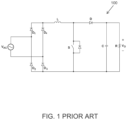
- a conventional AC-DC boost converter such as shown in FIG. 1 .
- the power converter has a sinusoidal input current.
- conventional AC-DC boost converter 100 includes an input diode bridge formed by rectifiers D 1 , D 2 , D 3 , and D 4 , boost inductor L, switching device S, boost diode D, filter capacitor C, and load R.
- load R is represented by a resistor.
- load R may also be another downstream converter (e.g., an isolated DC-DC converter that regulates a DC voltage supplied to the actual end-user load).
- AC-DC boost converter 100 may draw a nearly sinusoidal AC input current, resulting in a close-to-unity power factor.
- a high volumetric power density may be achieved by increasing the power converter's switching frequency, which tends to reduce the required size of the magnetic components (e.g., boost inductors and EMI filters).
- the magnetic components e.g., boost inductors and EMI filters.
- switching device S and boost diode D in AC-DC boost converter 100 are often implemented using silicon MOSFETs and silicon PN-junction diodes. When operated in hard-switching mode, silicon MOSFETs exhibit excessive turn-on and turn-off losses, as silicon diodes have severe reverse recovery losses.
- FIG. 2 shows AC-DC power converter 200 , configured for implementing soft-switching techniques.
- input diodes D 1 , D 2 , D 3 and D 4 , boost inductor L 1 , switching device S 1 , and boost diode D 5 form a conventional boost converter.
- AC-DC power converter 200 includes auxiliary circuit 205 formed by auxiliary inductor L 2 , auxiliary capacitor C 2 , auxiliary switching device S 2 and auxiliary diodes D 6 and D 7 .
- Auxiliary circuit 205 reduces the rate of current change
- ZVS zero-voltage switching
- AC-DC boost converter 100 implemented using SiC diodes, have become the preferred topology due to its favorable power-factor correction characteristic.
- a combination of S 1 MOSFETs and SiC diodes yield both cost-effectiveness and a reasonable trade-off between efficiency and power density. With their superior switching speed and reduced switching losses, as compared to Si MOSFETs, SiC MOSFETs are expected to provide even greater performance.
- FIG. 3 shows conventional totem-pole AC-DC boost converter 300 , which has become practical with switching devices S 1 and S 2 implemented by SiC MOSFETs. Having only two input rectifiers (i.e., input rectifiers D 1 and D 2 ), totem-pole AC-DC boost converter 300 operates in a substantially different manner than AC-DC boost converter 100 in that boost diode D's function is performed by the body diodes of switching devices S 1 and S 2 . In addition to topological differences, totem-pole AC-DC boost converter 300 allows bidirectional power flow, thereby expanding its field of application over AC-DC boost converter 100 . Thus, SiC MOSFETs achieve both increased switching frequency operation and high efficiency.
- SiC MOSFETs are still limited by (i) significant turn-on losses, and (ii) small reverse recovery loss in its body diode at high operating frequencies.
- soft-switching techniques are applied to smooth turn-on and turn-off transitions in SiC MOSFET switching devices of an AC-DC power converter (e.g., a totem-pole boost converter), thereby avoiding excessive turn-on and reverse-recovery losses when operating at a high switching frequency.
- the AC-DC power converter thus achieves high efficiency operation, high power density, bidirectional power flow, and reduced EMI noise.
- a power converter configured for coupling to an AC circuit and a DC circuit, includes: (a) a first inductor, which has a first terminal coupled to a first terminal of the AC circuit; (b) first and second rectifiers connected at a common node, forming a series circuit that is coupled in parallel to the DC circuit, with the common node coupled to a second terminal of the AC circuit; and (c) an active soft-switching cell that includes: (1) a second inductor; (2) first and second switches, forming, with the second inductor, a series circuit that is coupled in parallel to the series circuit of the first and second rectifiers; (3) a third switch; and (4) a first capacitor, forming, with the third switch, a series circuit that is coupled in parallel to the second inductor.
- the active soft-switching cell may reduce the reverse-recovery related losses of the AC-DC power converter.
- the active soft-switching cell also facilitates zero-voltage switching (ZVS) in the first, second and third switches.
- ZVS zero-voltage switching
- At least one of the switches may be provided by a silicon carbide (SiC) metal-oxide-semiconductor field-effect transistor (MOSFET).
- the power converter may be configured to operate in a bidirectional manner: e.g., the DC circuit may include a DC power source (e.g., a battery), or the AC-DC power converter may include a power inverter.
- the first and second rectifiers may be implemented by either passive diodes or synchronous rectifiers.
- the first inductor may be coupled to either (i) a common electrical node between the first switch and the second inductor, or (ii) a common electrical node between the second switch and the second inductor.
- an AC-DC power converter may be a multi-phase power converter configured for coupling to an AC circuit and a DC circuit.
- the AC circuit includes multiple terminals (“phase terminals”), each coupled to a phase of a multi-phase AC power source.
- the multi-phase power converter includes multiple component circuits (“phase legs”).
- each phase leg of the multi-phase power converter include: (a) a first inductor coupled to one of the phase terminals of the AC circuit; and (b) an active soft-switching cell that includes (1) a second inductor; (2) first and second switches forming, with the second inductor, a series circuit that is coupled in parallel to the DC circuit; (3) a third switch; and (4) a first capacitor forming, with the third switch, a series circuit that is coupled in parallel to the second inductor.
- the active soft-switching cell does not increase voltage and current stresses in conventional AC-DC power converters, the active soft-switching cell may be incorporated into most conventional AC-DC power converters to achieve the advantages of the present invention.
- FIG. 1 shows conventional AC-DC boost converter 100 .
- FIG. 2 shows conventional AC-DC power converter 200 , configured for implementing soft-switching techniques.
- FIG. 3 shows conventional AC-DC totem-pole boost converter 300 , which has become practical with switching devices S 1 and S 2 implemented by SiC MOSFETs.
- FIG. 4 shows totem-pole pulse-width-modulated (PWM) power-factor-correction (PFC) power converter 400 , according to one embodiment of the present invention.
- PWM pulse-width-modulated
- PFC power-factor-correction
- FIG. 5 shows circuit model 450 , representing an equivalent circuit for totem-pole PWM PFC power converter 400 during the positive half-cycle of input voltage V AC (i.e., V AC >0).
- FIGS. 6 A, 6 B, 6 C, 6 D, 6 E, 6 F, 6 G, 6 H and 6 I show the topological states of totem-pole PWM PFC power converter 400 over switching cycle T S during the positive half-cycle of input voltage V AC .
- FIG. 7 shows key power stage waveforms over switching cycle T S during the positive half-cycle of input voltage V AC (i.e., V AC >0).
- FIG. 8 shows circuit model 480 , representing an equivalent circuit for totem-pole PWM PFC power converter 400 during the negative half-cycle of input voltage V AC (i.e., V AC ⁇ 0).
- FIGS. 9 A, 9 B, 9 C, 9 D, 9 E, 9 F, 9 G, 9 H and 9 I show the topological states of totem-pole PWM PFC power converter 400 over switching cycle T S during the negative half-cycle of input voltage V AC .
- FIG. 10 shows key power stage waveforms over switching cycle T S during the negative half-cycle of input voltage V AC (i.e., V AC ⁇ 0).
- FIG. 11 shows active soft-switching cell 401 being incorporated into unidirectional AC-DC totem-pole power converter 1100 , in accordance with one embodiment of the present invention; unlike totem-pole PWM PFC power converter 400 , AC-DC totem-pole power converter 1100 has boost inductor L being coupled to the common electrical node between series inductor L S and auxiliary switch S A .
- FIG. 12 shows active soft-switching cell 401 being incorporated into bidirectional AC-DC totem-pole power converter 1200 , in accordance with one embodiment of the present invention; unlike totem-pole PWM PFC power converter 400 , diodes D 1 and D 2 are replaced by synchronous rectifiers S 3 and S 4 .
- FIG. 13 shows active soft-switching cell 401 being incorporated into AC-DC totem-pole power converter 1300 , according to one embodiment of the present invention; unlike totem-pole PWM PFC power converter 400 , diodes D PRE1 and D PRE2 charge the output DC link at start-up or when active soft-switching cell 401 is inactive, thereby bypassing active soft-switching cell 401 .
- FIG. 14 shows active soft-switching cell 401 being incorporated into bidirectional AC-DC totem-pole power converter 1400 , in accordance with one embodiment of the present invention; unlike totem-pole PWM PFC power converter 400 , diodes D 1 and D 2 are replaced by synchronous rectifiers S 3 and S 4 .
- FIG. 15 shows active soft-switching cell 401 being incorporated into bidirectional AC-DC totem-pole power converter 1500 , in accordance with one embodiment of the present invention; unlike bidirectional AC-DC totem-pole power converter 1400 , boost inductor L in AC-DC totem-pole power converter 1500 is coupled to the common electrical node between series inductor L S and auxiliary switch S A .
- FIG. 16 shows active soft-switching cell 401 being incorporated into multi-phase power converter 1600 , in accordance with one embodiment of the present invention.
- FIG. 17 shows multi-phase power converter 1700 , according to one embodiment of the present invention; unlike bidirectional 3-phase AC-DC power converter 1600 , each boost inductor boost inductor in multi-phase power converter 1700 is coupled to the common electrical node between the series inductor and the auxiliary switch in the corresponding active soft-switching cell.
- FIG. 4 shows a power converter 400 , according to one embodiment of the present invention.
- power converter 400 is a totem-pole pulse-width-modulated (PWM) power-factor-correction (PFC) power converter that performs rectification.
- PWM pulse-width-modulated
- PFC power-factor-correction
- totem-pole PWM PFC power converter 400 achieves a reduced switching loss.
- totem-pole PWM PFC power converter 400 is coupled between an AC circuit and a DC circuit and includes inductor L, series-connected rectifiers D 1 and D 2 , and active soft-switching cell 401 .
- Inductor L is coupled to one terminal of the AC circuit.
- Active soft-switching cell 401 includes inductor L S , switch S 1 , switch S 2 , switch S A , and capacitor C S .
- inductor L S and switch S 1 form a series circuit that is coupled in parallel to the series circuit of rectifiers D 1 and D 2 ;
- switch S A and capacitor C S form a series circuit 402 that is coupled in parallel to inductor L S ; and
- inductor L is coupled to either terminal of inductor L S .
- inductor L is coupled to a common electrical node between switch S 1 and inductor L S .
- at least one of switches S 1 , S 2 , and S A includes a silicon carbide metal-oxide-semiconductor field-effect transistor (MOSFET).
- MOSFET silicon carbide metal-oxide-semiconductor field-effect transistor
- totem-pole PWM PFC power converter 400 may further include a filter capacitor C connected in parallel with rectifiers D 1 and D 2 .
- switch S 1 or switch S 2 serves as boost switch or rectifier switch, according to the polarity of the AC circuit, and switch S A serves as an auxiliary switch.
- totem-pole PWM PFC power converter 400 differs from AC-DC totem-pole boost converter 300 of FIG. 3 by connecting series inductor L S between boost or rectifier switches S 1 and S 2 , so as to control the rate of change in current change
- switch S 2 serves as a “main” or “boost” switch, while switch S 1 serves as a rectifier switch; the roles of the switches reverse during the negative half cycle of the input AC voltage.
- switch S 1 serves as a rectifier switch; the roles of the switches reverse during the negative half cycle of the input AC voltage.
- Connected in parallel to series inductor L S are series-connected capacitor C S and auxiliary switch S A .
- Switches S 1 and S 2 , series inductor L S , auxiliary switch S A , and capacitor C S form soft-switching cell 401 , as indicated by dashed lines in FIG. 4 .
- switches S 1 , S 2 , and S A all operate with ZVS.
- the control signals for switches S 1 and S 2 are asserted in a non-overlapping manner, such that switches S 1 and S 2 do not conduct at the same time.
- the switch closes or is said to be “turned on.”
- the switch opens or is said to be “turned off.”
- either switch S 1 or switch S 2 serves as a rectifier switch which opens or closes simultaneously with switch S A .
- Inductor L S reduces the rate of current change when the rectifier switch opens.
- auxiliary switch S A The control signal for auxiliary switch S A is asserted simultaneously with the rectifier switch (i.e., switch S 1 , during the positive half of the line cycle, and switch S 2 , during the negative half of the line cycle).
- a short delay (“dead time”) is introduced between de-assertion of the control signal on the main switch and assertions of the control signals on the rectifier switch and auxiliary switch S A .
- the portion of the input current flowing through series inductor L S (i.e., i LS ) is diverted from the main switch and redirected to flow through the body diodes of the rectifier switch and auxiliary switch S A , thereby discharging both the rectifier switch's and auxiliary switch S A 's parasitic output capacitances to allow closing both the rectifier switch and auxiliary switch S A under ZVS condition.
- current i LS in series inductor L S still flows through the body diode of the rectifier switch, discharging the main switch's parasitic output capacitance to create a ZVS condition for the main switch to turn on.
- the switching frequency of switches S 1 , S 2 , and S A is much higher than the line frequency of input voltage V AC . Consequently, for the purpose of the following analysis, within the time frame of a few switching cycles, input voltage V AC may be seen as a substantially constant voltage V IN . Also, as the inductance of boost inductor L and the capacitance of filter capacitor C are both large, as compared to the inductances and the capacitances of other circuit elements in totem-pole PWM PFC power converter 400 , both the ripples in inductor current i L and the ripples in the voltage across filter capacitor C may be deemed insignificant. Accordingly, the voltage across output filter capacitor C may be represented by constant voltage source Vo.
- switches S 1 , S 2 and S A each have an insignificant resistance in their respective conducting states (“on-resistance”). During their conducting states, each of these switches may be considered a short circuit. However, the parasitic output capacitances of these switches (i.e., capacitors C OSS1 , C OSS2 and C OSSA ) and the reverse-recovery charge in each of their body diodes are not neglected.
- FIGS. 5 and 8 show circuit models 450 and 480 , representing the equivalent circuits for totem-pole PWM PFC power converter 400 under, respectively, the positive half-cycle (i.e., V AC >0) and the negative half-cycle (i.e., V AC ⁇ 0) of input voltage V AC .
- FIGS. 6 A- 6 I show the topological states of totem-pole PWM PFC power converter 400 over switching cycle T S during the positive half-cycle of input voltage V AC (i.e., V AC >0).
- FIG. 7 shows key power stage waveforms over switching cycle T S during the positive half-cycle of input voltage V AC (i.e., V AC >0).
- FIGS. 9 A- 9 I show the topological states of totem-pole PWM PFC power converter 400 over switching cycle T S during the negative half-cycle of input voltage V AC (i.e., V AC ⁇ 0).
- FIG. 10 shows key power stage waveforms over switching cycle T S during the negative half-cycle of input voltage V AC (i.e., V AC ⁇ 0).
- main switch S 2 is turned on—but is about to be turned off at time T 1 —booth boost inductor current i L and series inductor current i LS flow in main switch S 2 , while rectifier switch S 1 and auxiliary switch S A are turned off. Since the inductance in boost inductor L is much larger than the inductance of series inductor L S , substantially all of input voltage V IN is imposed across boost inductor L.
- boost inductor current i L and series inductor current i LS increase linearly according to:
- FIG. 6 B shows the topological state of totem-pole PWM PFC power converter 400 during interval [T 1 , T 2 ].
- series inductor current i LS which is substantially equal to boost inductor current i L at time T 1 , begins to charge parasitic output capacitance C OSS2 of main switch S 2 .
- voltage V S2 across main switch S 2 begins to increase.
- Equation (2) provides:
- Interval [T 1 , T 2 ] is expected to be very short relative to the switching cycle T S , as parasitic output capacitances C OSS1 and C OSS2 of rectifier and main switches S 1 and S 2 are typically less than 1 nF.
- FIG. 6 ( c ) shows the topological state of totem-pole PWM PFC power converter 400 during interval [T 2 , T 3 ].
- T 2 when parasitic output capacitance C OSS1 of rectifier switch S 1 has fully discharged, the body diode of rectifier switch S 1 becomes conducting and carries boost inductor current i L , thereby transferring power from the input voltage source to the output load.
- the voltage across boost inductor L equals the difference between output voltage V O and input voltage V IN , so that boost inductor current i L decreases linearly according to
- FIG. 6 D shows the topological state of totem-pole PWM PFC power converter 400 during interval [T 3 , T 4 ].
- both auxiliary switch S A and rectifier switch S 1 turn on under ZVS condition.
- the commutation cycle is complete and totem-pole PWM PFC power converter 400 enters the topological states for interval [T 3 , T 5 ] in which substantially all of boost inductor current i L is delivered to the output.
- FIG. 6 E shows the topological state of totem-pole PWM PFC power converter 400 during interval [T 4 , T 5 ].
- auxiliary switch S A closes at time T 3
- series inductor current i LS crosses zero and turns negative
- current i SA in auxiliary switch S A reverses polarity to turn positive.
- FIG. 6 F shows the topological state of totem-pole PWM PFC power converter 400 during interval [T 5 , T 6 ].
- both rectifier switch S 1 and auxiliary switch S A turn off.
- Voltage V S1 across rectifier switch S 1 remains small, as the input current still flows through the body diode of switch S 1 .
- parasitic output capacitance C OSSA of auxiliary switch S A begins to charge.
- FIG. 6 G shows the topological state of totem-pole PWM PFC power converter 400 during interval [T 6 , T 7 ].
- parasitic output capacitance C OSS2 of main switch S 2 has discharged completely, so that series inductor current i LS flows entirely through the body diode of main switch S 2 .
- Boost inductor current i L and series inductor current i LS are substantially equal in magnitude but of opposite polarity.
- the body diode of rectifier switch S 1 briefly carries a peak current that is twice the magnitude of the input current (i.e., the boost inductor current i L ).
- the rate of decrease in current of rectifier switch S 1 is controlled by series inductor L S . Accordingly, the rectifier recovered charge and its associated loss may be reduced by selecting a suitable inductance for series inductor L S . Generally, a larger inductance—which gives a lower rate of current decrease—results in a higher reduction of the reverse recovery associated losses.
- FIG. 6 H shows the topological state of totem-pole PWM PFC power converter 400 during interval [T 7 , T 8 ].
- switch S 2 should turn on before series inductor current i LS polarity turns positive.
- main switch S 2 turns on immediately prior to series inductor current i LS turns positive.
- parasitic output capacitance C OSS2 of main switch S 2 may be fully or partially charged and thus the ZVS condition would not be achieved.
- boost inductor current i L increases linearly at the rate of
- the inductance of series inductor L S is preferably much less than the inductance of boost inductor L, so that rate of change in series inductor current i LS is substantially higher than the rate of change in boost inductor current i L .
- FIG. 6 I shows the topological state of totem-pole PWM PFC power converter 400 during interval [T 8 , T 9 ].
- Boost inductor current i L and series-inductor current i LS become equal at time T 8 , so that the current in rectifier switch S 1 becomes zero.
- parasitic output capacitance C OSS1 of rectifier switch S 1 begins to charge.
- Equation (2) an increase in voltage V S1 across rectifier switch S 1 is accompanied by a decrease in voltage V SA across auxiliary switch S A , i.e., discharging parasitic output capacitance C OSSA of auxiliary switch S A and a decrease in the voltage imposed across series inductor L S .
- series inductor current i LS eventually decreases to equal boost inductor current i L .
- Voltage V SA across auxiliary switch S A becomes equal to series capacitor voltage V CS , such that the voltage across series inductor L S becomes practically zero, and output voltage V O is imposed substantially entirely across rectifier switch S 1 .
- FIG. 7 shows that the voltage stresses on main switch S 2 , rectifier switch S 1 , and auxiliary switch S A is sum of output voltage V O and voltage V CS across series capacitor C S (i.e., V O +V CS ), so that the stresses on main switch S 2 and rectifier switch S 1 is higher than the stresses on the corresponding switches in the conventional, hard-switched boost converter (e.g., AC-DC totem-pole boost converter 300 of FIG. 3 ).
- the selection of a suitable capacitance for series capacitor C S ensures a reasonable value for voltage V CS , which keeps the voltage stresses on the switches to within reasonable limits.
- intervals [T 1 , T 3 ] and [T 5 , T 8 ] are short relative to the intervals in which main switch S 2 and rectifier switch S 1 are conducting.
- series capacitor C S discharges through series inductor current i LS .
- Series inductor current i LS reverses polarity at time T 4 to charge series capacitor C S during interval [T 4 , T 6 ].
- the current in series capacitor C S has a substantially constant slope
- I L be the average value for boost inductor current i L .
- V O V I ⁇ N V O V I ⁇ N
- Equation (6) may therefore be rewritten as:
- V C ⁇ S ⁇ L S ⁇ 2 ⁇ I L ⁇ f S ⁇ V O V I ⁇ N ( 8 ) where f S is the switching frequency.
- voltage V CS is maximum at full load (i.e., maximum I L ) and at the lowest line voltage (i.e., at minimum V IN ).
- series capacitor voltage V CS may be reduced by reducing the L S *f S product.
- Totem-pole rectifiers are often used in input current-shaping applications, with the objectives being reducing harmonic contents and improving the power factor of the line current.
- output voltage V O is required to be maintained substantially constant, while the duty cycle of the totem-pole rectifier varies from 0 to
- the input current shape preferably follows the input voltage shape.
- voltage V CS is substantially constant throughout the line cycle.
- FIG. 8 shows circuit model 480 , representing the equivalent circuit for totem-pole PWM PFC power converter 400 during the negative half-cycle of input voltage V AC (i.e., V AC ⁇ 0).
- FIGS. 9 A- 9 I show the topological states of totem-pole PWM PFC power converter 400 over switching cycle T S during the negative half-cycle of input voltage V AC .
- FIG. 10 shows key power stage waveforms over switching cycle T S during the negative half-cycle of input voltage V AC (i.e., V AC ⁇ 0).
- active soft-switching cell 401 of totem-pole PWM PFC power converter 400 operates substantially as explained above with respect to FIGS. 6 A- 6 I and FIG.
- FIGS. 9 A- 9 I and FIG. 10 are therefore omitted.
- main switch S 1 when main switch S 1 is turned on, no current flow through series inductor L S , as input voltage V AC is imposed entirely across boost inductor L.
- FIGS. 6 A and 6 I to FIGS. 9 A and 9 I for intervals [T 0 , T 1 ] and [T 8 , T 9 ]).
- the peak current in series inductor L S is approximately twice as large in the negative half-cycle, as compared to the positive half-cycle.
- the control circuit for totem-pole PWM PFC power converter 400 may be implemented in the same manner as its conventional “hard-switched” totem-pole rectifier counterpart, so long as an additional gate-driver circuit is provided for auxiliary switch S A .
- totem-pole PWM PFC power converter 400 may be implemented using any suitable control technique (e.g., average-current control, peak-current control, or hysteretic control).
- FIG. 11 shows active soft-switching cell 401 being incorporated into unidirectional AC-DC totem-pole power converter 1100 , in accordance with one embodiment of the present invention; unlike PWM PFC power converter 400 , AC-DC totem-pole power converter 1100 has boost inductor L being coupled to the common electrical node between series inductor L S and auxiliary switch S A .
- boost inductor L may be connected to either the common electrical node between series inductor L S and switch S 2 or the common electrical node between series inductor L S and switch S 1 . This result may be seen from the equivalent circuits for each configuration in the positive and negative half-cycles of input voltage V AC .
- the equivalent circuits for AC-DC totem pole power converter 1100 are model 480 of FIG. 8 under the positive half-cycle (i.e., V AC >0), with switch S 2 as the rectifier switch, and model 450 of FIG. 5 under the negative half-cycle of input voltage V AC (i.e., V AC ⁇ 0), with switch S 1 as the rectifier switch.
- totem-pole PWM PFC power converter 400 in the positive and negative half-cycles operate substantially identically to AC-DC totem-pole power converter 1100 in the negative and positive half-cycles, respectively.
- FIG. 12 shows active soft-switching cell 401 being incorporated into bidirectional AC-DC totem-pole power converter 1200 , in accordance with one embodiment of the present invention; unlike totem-pole PWM PFC power converter 400 , diodes D 1 and D 2 are replaced by switches or synchronous rectifiers S 3 and S 4 . Synchronous rectifiers (e.g., switches S 3 and S 4 ) have much lower voltage drops than passive diodes D 1 and D 2 , thus providing increased converter efficiency. Note that, diodes D 1 and D 2 in totem-pole configuration in any of the configurations herein may be replaced by synchronous rectifiers to achieve the converter efficiency advantage.
- FIG. 13 shows active soft-switching cell 401 being incorporated into AC-DC totem-pole power converter 1300 , according to one embodiment of the present invention; unlike totem-pole PWM PFC power converter 400 , diodes D PRE1 and D PRE2 charge the output DC link (e.g., across filter capacitor C) at start-up or when active soft-switching cell 401 is inactive, thereby bypassing active soft-switching cell 401 .
- Diodes D PRE1 and D PRE2 are typically silicon devices. Once the DC link is charged, diodes D PRE1 and D PRE2 would no longer conduct, as current from the AC source would go through active soft-switching cell 401 .
- FIG. 14 shows active soft-switching cell 401 being incorporated into bidirectional AC-DC totem-pole power converter 1400 , in accordance with one embodiment of the present invention. Note also that diodes D 1 and D 2 are replaced by synchronous rectifiers S 3 and S 4 to take advantage of the higher converter efficiency discussed above.
- FIG. 15 shows active soft-switching cell 401 being incorporated into bidirectional AC-DC totem-pole power converter 1500 , in accordance with one embodiment of the present invention; unlike bidirectional AC-DC totem-pole power converter 1400 , boost inductor L in AC-DC totem-pole power converter 1500 is coupled to the common electrical node between series inductor L S and auxiliary switch S A . As discussed above, these configurations operate in a substantially equivalent manner.
- FIG. 16 shows multi-phase power converter 1600 , according to one embodiment of the present invention.
- multi-phase power converter 1600 is a bidirectional 3-phase AC-DC power converter that incorporates active soft-switching cell 401 of FIG. 4 .
- Multi-phase power converter 1600 is coupled between an AC circuit and a DC circuit.
- AC circuit may be a multi-phase AC source, it includes multiple phase terminals.
- the DC circuit may be a resistive load or a DC power source.
- Multi-phase power converter 1600 includes multiple component circuits (“phase legs”) each coupled to a phase terminal of the AC circuit.
- Each phase leg of multi-phase power converter 1600 includes an inductor (i.e., inductor L 1 , L 2 or L 3 ), which couples the phase leg to the corresponding phase terminal, and an active soft-switching cell.
- the active soft-switching cell of each phase leg includes (i) a series inductor (i.e., inductor L S1 , L S2 or L S3 ), (ii) first and second switches (i.e., switches S 1 and S 2 , switches S 3 and S 4 , or switches S 5 and S 6 ), (iii) an auxiliary switch (i.e., switch S A1 , S A2 or S A3 ) and (iv) an auxiliary capacitor (i.e., C S1 , C S2 , or C S3 ).
- any of the switches may open under a ZVS condition. At least one of the switches may be a carbide MOSFET.
- the series inductor and the first and second switches form a series circuit across the DC circuit.
- either the first switch i.e., first switch S 1 , S 3 or S 5
- the second switch i.e., S 2 , S 4 or S 6
- serves as a rectifier switch that opens and closes simultaneously with the auxiliary switch i.e., switch S A1 , S A2 or S A3 ).
- the series inductor i.e., series inductor L S1 , L S2 or L S3 . reduces the rate of current change when the rectifier switch opens.
- the reduced rate of current change may reduce reverse recovery loss in the rectifier switch.
- a 3-phase AC source provides 3 lines of voltages V A , V B , and V C .
- the 3 lines may be provided from a Y- or WYE connection or a delta connection.
- each leg of the three phases include an instance of active soft-switching cell 401 coupled to a corresponding boost inductor (i.e., boost inductors L 1 , L 2 , and L 3 ).
- the number of phase legs may be any suitable number required to deliver the desired power, according to the application. Note that, in a multi-phase power converter, the phase-return path for each phase leg is provided by other phase legs, such that totem-pole rectifier stage (e.g., diodes or synchronous rectifiers) is not required.
- FIG. 17 shows multi-phase power converter 1700 , according to one embodiment of the present invention.
- multi-phase power converter 1700 is coupled between an AC circuit and a DC circuit.
- the AC circuit may be a multi-phase AC source, it includes multiple phase terminals.
- the DC circuit may be a resistive load or a DC power source.
- each boost inductor (i.e., inductor L 1 , L 2 , or L 3 ) in multi-phase power converter 1700 is coupled to the common electrical node between the series inductor (i.e., series inductor L S1 , L S2 , or L S3 ) and the auxiliary switch (i.e., switch S A1 , S A2 , or S A3 ) in the corresponding active soft-switching cell.
- the series inductor and the first and second switches form a series circuit across the DC circuit.
- either the first switch i.e., first switch S 1 , S 3 or S 5
- the second switch i.e., S 2 , S 4 or S 6
- the auxiliary switch i.e., switch S A1 , S A2 or S A3
- Any of the switches may open under a ZVS condition.
- At least one of the switches may be a carbide MOSFET.
- the series inductor i.e., series inductor L S1 , L S2 or L S3
- the number of phase terminals and phase legs may be any suitable number required to deliver the desired power, according to the application.
- the present invention substantially reduces the switching losses in an AC-DC power conversion system caused by the turn-on characteristics of a main switch and the reverse-recovery characteristic of a rectifier, using an active soft-switching cell, as that described in the embodiments above. Specifically, the reverse-recovery related losses are reduced by the series inductor in the active soft-switching cell, which reduces the rate of current change in the body diode of the rectifier switch during its turn-off.
- the switches in the active soft-switching cell may operate under ZVS conditions.
Abstract
A circuit technique substantially reduces the switching losses in an AC-DC power conversion system caused by turn-on characteristics of a main switch and the reverse-recovery characteristic of a rectifier. The losses are reduced by using an active soft-switching cell having a series inductor, a series capacitor, a main switch, a rectifier switch, and an auxiliary switch. The reverse-recovery related losses are reduced by the series inductor connected between the main and rectifier switches to control the rate of current change in the body diode of the rectifier switch during its turn-off. The main switch, the rectifier switch, and the auxiliary switch operate under zero-voltage switching (ZVS) conditions.
Description
The present invention generally relates to power conversion systems. More particularly, the present invention relates to bidirectional AC-DC power conversion circuits with soft switching capability.
To interface with the AC utility system (i.e., the public power grid), power supplies are required to comply with input-current harmonic standards. In this regard, the limits for low-frequency harmonic distortion are quite stringent and, generally, they are met by imposing a sinusoidal input current to the power converter. In addition, high efficiency, high power density and low electromagnetic interference (EMI) noise are also important considerations. A power converter that interfaces with the AC utility system and achieves low harmonic distortion resembles a resistive load to the AC power supply—i.e., its input current follows the input voltage waveform. One example of such a power converter is a conventional AC-DC boost converter, such as shown in FIG. 1 . As a resistive load, the power converter has a sinusoidal input current.
As shown in FIG. 1 , conventional AC-DC boost converter 100 includes an input diode bridge formed by rectifiers D1, D2, D3, and D4, boost inductor L, switching device S, boost diode D, filter capacitor C, and load R. In FIG. 1 , load R is represented by a resistor. However, load R may also be another downstream converter (e.g., an isolated DC-DC converter that regulates a DC voltage supplied to the actual end-user load). Under suitable control, AC-DC boost converter 100 may draw a nearly sinusoidal AC input current, resulting in a close-to-unity power factor.
Besides aiming for a high power factor, a designer may also seek to achieve an optimized trade-off between efficiency and power density. A high volumetric power density may be achieved by increasing the power converter's switching frequency, which tends to reduce the required size of the magnetic components (e.g., boost inductors and EMI filters). However, operating at a high switching frequency increases switching losses, which decreases efficiency. In the prior art, switching device S and boost diode D in AC-DC boost converter 100 are often implemented using silicon MOSFETs and silicon PN-junction diodes. When operated in hard-switching mode, silicon MOSFETs exhibit excessive turn-on and turn-off losses, as silicon diodes have severe reverse recovery losses. As a result, an increased switching frequency significantly deteriorates AC-DC boost converter 100's power conversion efficiency. To overcome the severe loss at a high switching frequency, soft-switching techniques are developed to smooth transitions in switching device S during turn-on and turn-off events. The resulting reduced rate of change in rectifier diode currents advantageously reduces both the reverse recovery current loss and any related boost diode loss.
in boost diode D5 during its turn-off event, so as to substantially remove the reverse recovery loss and to allow a soft turn-on transition in switching device S1 (i.e., zero-voltage switching (ZVS)). ZVS thus provides a significant efficiency improvement, even at an increased switching frequency that achieves a higher power density. Until recently, soft-switching circuits were implemented in most boost converters to reduce reverse recovery losses in the boost diode. Recently, however, wide-band-gap materials (e.g., silicon carbide (SiC)) have yielded Schottky barrier diodes that have substantially no reverse-recovery losses. As a result, AC-
Today, SiC MOSFETs are still limited by (i) significant turn-on losses, and (ii) small reverse recovery loss in its body diode at high operating frequencies.
According to one embodiment of the present invention, soft-switching techniques are applied to smooth turn-on and turn-off transitions in SiC MOSFET switching devices of an AC-DC power converter (e.g., a totem-pole boost converter), thereby avoiding excessive turn-on and reverse-recovery losses when operating at a high switching frequency. The AC-DC power converter thus achieves high efficiency operation, high power density, bidirectional power flow, and reduced EMI noise.
According to one embodiment, a power converter, configured for coupling to an AC circuit and a DC circuit, includes: (a) a first inductor, which has a first terminal coupled to a first terminal of the AC circuit; (b) first and second rectifiers connected at a common node, forming a series circuit that is coupled in parallel to the DC circuit, with the common node coupled to a second terminal of the AC circuit; and (c) an active soft-switching cell that includes: (1) a second inductor; (2) first and second switches, forming, with the second inductor, a series circuit that is coupled in parallel to the series circuit of the first and second rectifiers; (3) a third switch; and (4) a first capacitor, forming, with the third switch, a series circuit that is coupled in parallel to the second inductor. In one embodiment, the active soft-switching cell may reduce the reverse-recovery related losses of the AC-DC power converter. The active soft-switching cell also facilitates zero-voltage switching (ZVS) in the first, second and third switches. At least one of the switches may be provided by a silicon carbide (SiC) metal-oxide-semiconductor field-effect transistor (MOSFET).
In one embodiment, the power converter may be configured to operate in a bidirectional manner: e.g., the DC circuit may include a DC power source (e.g., a battery), or the AC-DC power converter may include a power inverter. The first and second rectifiers may be implemented by either passive diodes or synchronous rectifiers. The first inductor may be coupled to either (i) a common electrical node between the first switch and the second inductor, or (ii) a common electrical node between the second switch and the second inductor.
According to some embodiment of the present invention, an AC-DC power converter may be a multi-phase power converter configured for coupling to an AC circuit and a DC circuit. The AC circuit includes multiple terminals (“phase terminals”), each coupled to a phase of a multi-phase AC power source. The multi-phase power converter includes multiple component circuits (“phase legs”). In one embodiment, each phase leg of the multi-phase power converter include: (a) a first inductor coupled to one of the phase terminals of the AC circuit; and (b) an active soft-switching cell that includes (1) a second inductor; (2) first and second switches forming, with the second inductor, a series circuit that is coupled in parallel to the DC circuit; (3) a third switch; and (4) a first capacitor forming, with the third switch, a series circuit that is coupled in parallel to the second inductor.
As the active soft-switching cell according to the present invention does not increase voltage and current stresses in conventional AC-DC power converters, the active soft-switching cell may be incorporated into most conventional AC-DC power converters to achieve the advantages of the present invention.
The present invention is better understood upon consideration of the following detailed description and the accompanying drawings.
The present invention will now be described more specifically with reference to the following embodiments. It is to be noted that the following descriptions of embodiments of this disclosure are presented herein for purpose of illustration and description only. It is not intended to be exhaustive or to be limited to the precise form disclosed.
As shown in FIG. 4 , totem-pole PWM PFC power converter 400 differs from AC-DC totem-pole boost converter 300 of FIG. 3 by connecting series inductor LS between boost or rectifier switches S1 and S2, so as to control the rate of change in current change
in the body diode of the rectifier switch when the rectifier switch is open. (During the positive half of each cycle of the input AC voltage, switch S2 serves as a “main” or “boost” switch, while switch S1 serves as a rectifier switch; the roles of the switches reverse during the negative half cycle of the input AC voltage.) Connected in parallel to series inductor LS are series-connected capacitor CS and auxiliary switch SA. Switches S1 and S2, series inductor LS, auxiliary switch SA, and capacitor CS form soft-switching
According to one embodiment of the present invention, switches S1, S2, and SA all operate with ZVS. In addition, the control signals for switches S1 and S2 are asserted in a non-overlapping manner, such that switches S1 and S2 do not conduct at the same time. In this detailed description, when the control signal of a switch is asserted, the switch closes or is said to be “turned on.” Conversely, when the control signal of a switch is de-asserted, the switch opens or is said to be “turned off.” In one embodiment, at any given time, either switch S1 or switch S2 serves as a rectifier switch which opens or closes simultaneously with switch SA. Inductor LS reduces the rate of current change when the rectifier switch opens. The control signal for auxiliary switch SA is asserted simultaneously with the rectifier switch (i.e., switch S1, during the positive half of the line cycle, and switch S2, during the negative half of the line cycle). A short delay (“dead time”) is introduced between de-assertion of the control signal on the main switch and assertions of the control signals on the rectifier switch and auxiliary switch SA. In this embodiment, when the main switch is turned off, the portion of the input current flowing through series inductor LS (i.e., iLS) is diverted from the main switch and redirected to flow through the body diodes of the rectifier switch and auxiliary switch SA, thereby discharging both the rectifier switch's and auxiliary switch SA's parasitic output capacitances to allow closing both the rectifier switch and auxiliary switch SA under ZVS condition. When the rectifier switch and auxiliary switch SA subsequently turn off, however, current iLS in series inductor LS still flows through the body diode of the rectifier switch, discharging the main switch's parasitic output capacitance to create a ZVS condition for the main switch to turn on. Without the discharging of the main switch's parasitic output capacitance, as is the case in prior art topologies, turning on the main switch results in a large turn-on loss. In addition, when the main switch turns on, series inductor LS lowers the rate of change in the rectifier switch current, which significantly reduces the rectifier switch's reverse-recovery loss.
Note that the following analysis uses totem-pole AC PWM PFC power converter 400 as an example. The analysis would be the same for a bidirectional operation, in which resistive load R in FIG. 4 is replaced by a DC voltage source (e.g., a battery). In that bidirectional configuration, filter capacitor C is optional. See, e.g., FIG. 14 , showing bidirectional AC-DC power converter 1400.
In totem-pole PWM PFC power converter 400, the switching frequency of switches S1, S2, and SA is much higher than the line frequency of input voltage VAC. Consequently, for the purpose of the following analysis, within the time frame of a few switching cycles, input voltage VAC may be seen as a substantially constant voltage VIN. Also, as the inductance of boost inductor L and the capacitance of filter capacitor C are both large, as compared to the inductances and the capacitances of other circuit elements in totem-pole PWM PFC power converter 400, both the ripples in inductor current iL and the ripples in the voltage across filter capacitor C may be deemed insignificant. Accordingly, the voltage across output filter capacitor C may be represented by constant voltage source Vo. Similarly, switches S1, S2 and SA each have an insignificant resistance in their respective conducting states (“on-resistance”). During their conducting states, each of these switches may be considered a short circuit. However, the parasitic output capacitances of these switches (i.e., capacitors COSS1, COSS2 and COSSA) and the reverse-recovery charge in each of their body diodes are not neglected. Based on these considerations, FIGS. 5 and 8 show circuit models 450 and 480, representing the equivalent circuits for totem-pole PWM PFC power converter 400 under, respectively, the positive half-cycle (i.e., VAC>0) and the negative half-cycle (i.e., VAC<0) of input voltage VAC.
Based on circuit model 450 of FIG. 5 , FIGS. 6A-6I show the topological states of totem-pole PWM PFC power converter 400 over switching cycle TS during the positive half-cycle of input voltage VAC (i.e., VAC>0). FIG. 7 shows key power stage waveforms over switching cycle TS during the positive half-cycle of input voltage VAC (i.e., VAC>0).
Likewise, based on circuit model 480 of FIG. 8 , FIGS. 9A-9I show the topological states of totem-pole PWM PFC power converter 400 over switching cycle TS during the negative half-cycle of input voltage VAC (i.e., VAC<0). FIG. 10 shows key power stage waveforms over switching cycle TS during the negative half-cycle of input voltage VAC (i.e., VAC<0).
As shown in FIG. 6A , during interval [T0, T1], main switch S2 is turned on—but is about to be turned off at time T1—booth boost inductor current iL and series inductor current iLS flow in main switch S2, while rectifier switch S1 and auxiliary switch SA are turned off. Since the inductance in boost inductor L is much larger than the inductance of series inductor LS, substantially all of input voltage VIN is imposed across boost inductor L. Therefore, (i) voltage VO across filter capacitor C is imposed across main switch S2, (ii) voltage VCS across series capacitor CS is imposed across auxiliary switch SA, and (iii) input voltage VIN is imposed across series-connected boost inductor L and series inductor LS. Hence, boost inductor current iL and series inductor current iLS increase linearly according to:
where L and LS in this and other equations represent the inductances of boost inductor L and series inductor LS, respectively.
V S1 −V CS +V SA +V S2 =V O (2)
-
- where VS1, VCS, VSA and VS2 are voltages across rectifier switch S1, series capacitor CS, auxiliary switch SA, and main switch S2, respectively
As the capacitance of series capacitor CS is selected to be much larger than the parasitic output capacitance of the switches (i.e., CS>>COSS1, COSS2, and COSSA), voltage VCS across series capacitor CS can be deemed constant. Thus, Equation (2) provides:
In other words, during interval [T1, T2], parasitic output capacitance COSS1 of rectifier switch S1 and parasitic output capacitance COSSA of auxiliary switch SA are discharging, while parasitic output capacitance COSS2 of main switch S2 is charging. Furthermore, when voltage VSA across switch SA reaches 0 volts, the body diode of auxiliary switch SA turns on, and the voltages across rectifier switch S1 and main switch S2 is given by:
as shown in
At the same time, the body diode of auxiliary switch SA conducts current iLS, so that voltage VCS across series capacitor CS is imposed across series inductor LS. Consequently, series inductor current iLS decreases linearly, according to
Thus, as shown in Equation (5), the rate of decrease in current of rectifier switch S1 is controlled by series inductor LS. Accordingly, the rectifier recovered charge and its associated loss may be reduced by selecting a suitable inductance for series inductor LS. Generally, a larger inductance—which gives a lower rate of current decrease—results in a higher reduction of the reverse recovery associated losses.
During interval [T6, T8], boost inductor current iL increases linearly at the rate of
while series inductor current iLS increases linearly at the rate of
The inductance of series inductor LS is preferably much less than the inductance of boost inductor L, so that rate of change in series inductor current iLS is substantially higher than the rate of change in boost inductor current iL.
The derivation of how circuit parameters in totem-pole PWM PFC power converter 400 depend on voltage VCS may be simplified by recognizing that intervals [T1, T3] and [T5, T8] (i.e., the commutation periods) are short relative to the intervals in which main switch S2 and rectifier switch S1 are conducting. As shown in FIG. 7 , during interval [T1, T4], series capacitor CS discharges through series inductor current iLS. Series inductor current iLS reverses polarity at time T4 to charge series capacitor CS during interval [T4, T6]. Except during the commutation periods (i.e., intervals [T1, T3] and [T5, T8]) and during interval [T8, T9], the current in series capacitor CS has a substantially constant slope
(During interval [T8, T9], the current in series capacitor CS is substantially zero.) Let IL be the average value for boost inductor current iL. To achieve ZVS in main switch S2 and auxiliary switch SA (i.e., at time T3, when series inductor current iLS equals −IL) and in rectifier switch S1 (i.e., at time T5, when series inductor current iLS equals IL),
over interval [T3, T5] provides:
where D′ is the duty cycle of rectifier switch S1, TS is the duration of the switching cycle and interval [T3, T5] is substantially period TON, when rectifier switch S1 is turned on. For a lossless totem-pole power stage in which the current commutation intervals (i.e., [T1, T3] and [T5,T8]) are much shorter than TON, voltage conversion ratio
is given by:
where IO is the average value of the output load current. Equation (6) may therefore be rewritten as:
where fS is the switching frequency.
Therefore, according to Equation (8), voltage VCS is maximum at full load (i.e., maximum IL) and at the lowest line voltage (i.e., at minimum VIN). For given input and output specifications (i.e., for given maximum IL and output voltage VO), series capacitor voltage VCS may be reduced by reducing the LS*fS product.
Totem-pole rectifiers are often used in input current-shaping applications, with the objectives being reducing harmonic contents and improving the power factor of the line current. In any such a current-shaping application, even though input voltage VIN varies during the line cycle, output voltage VO is required to be maintained substantially constant, while the duty cycle of the totem-pole rectifier varies from 0 to
In a PFC rectifier, the input current shape preferably follows the input voltage shape. Thus, according to Equation (8), voltage VCS is substantially constant throughout the line cycle.
The control circuit for totem-pole PWM PFC power converter 400 may be implemented in the same manner as its conventional “hard-switched” totem-pole rectifier counterpart, so long as an additional gate-driver circuit is provided for auxiliary switch SA. Specifically, for input current-shaping applications, totem-pole PWM PFC power converter 400 may be implemented using any suitable control technique (e.g., average-current control, peak-current control, or hysteretic control).
In FIG. 16 , a 3-phase AC source provides 3 lines of voltages VA, VB, and VC. The 3 lines may be provided from a Y- or WYE connection or a delta connection. As shown in FIG. 16 , each leg of the three phases include an instance of active soft-switching cell 401 coupled to a corresponding boost inductor (i.e., boost inductors L1, L2, and L3). The number of phase legs may be any suitable number required to deliver the desired power, according to the application. Note that, in a multi-phase power converter, the phase-return path for each phase leg is provided by other phase legs, such that totem-pole rectifier stage (e.g., diodes or synchronous rectifiers) is not required.
The present invention substantially reduces the switching losses in an AC-DC power conversion system caused by the turn-on characteristics of a main switch and the reverse-recovery characteristic of a rectifier, using an active soft-switching cell, as that described in the embodiments above. Specifically, the reverse-recovery related losses are reduced by the series inductor in the active soft-switching cell, which reduces the rate of current change in the body diode of the rectifier switch during its turn-off. The switches in the active soft-switching cell may operate under ZVS conditions.
While various embodiments of the present invention have been described above, the present invention has been presented only by way of illustrative examples in these embodiments, and has not been limited. Thus, the breadth and scope of the present invention should not be limited by any of the above described embodiments but should instead be defined only in accordance with the following claims and their equivalents.
Claims (18)
1. A power converter configured for coupling to (i) an AC circuit having first and second terminals and (ii) a DC circuit, comprising: a first inductor, having first and second terminals, the first terminal of the first inductor being coupled to the first terminal of the AC circuit; first and second rectifiers connected at a common node, wherein the first and second rectifiers form a series circuit coupled in parallel to the DC circuit, and wherein the common node is coupled to the second terminal of the AC circuit; an active soft-switching cell, comprising: a second inductor having first and second terminals; first and second switches, wherein the first switch, the second inductor and the second switch form a series circuit coupled in parallel to the series circuit of the first and the second rectifiers; a third switch; and a first capacitor, wherein the third switch and the first capacitor form a series circuit that is coupled in parallel to the second inductor; and wherein the second terminal of the first inductor is coupled to the first terminal or the second terminal of the second inductor, wherein one of the first and second switch serves as a rectifier switch that opens and closes simultaneously with the third switch, and wherein the second inductor has an inductance that reduces the rate of current change when the rectifier switch opens.
2. The power converter of claim 1 , wherein at least one of the switches comprises a silicon carbide metal-oxide-semiconductor field-effect transistor (MOSFET).
3. The power converter of claim 1 , wherein the power converter is configured to operate in a bidirectional manner.
4. The power converter of claim 1 , wherein the AC circuit comprises an AC power source, and wherein the DC circuit comprises at least one of: a resistive load and a DC power source.
5. The power converter of claim 1 , further comprising a filter capacitor connected in parallel to the first and second rectifiers.
6. The power converter of claim 1 , wherein one or more of the first and second rectifiers comprise a synchronous rectifier.
7. The power converter of claim 1 , wherein the reduced rate of current change reduces reverse recovery loss in the rectifier switch.
8. The power converter of claim 1 , wherein one or more of the first switch, the second switch and the third switch open under a zero-voltage switching condition.
9. The power converter of claim 1 , wherein the first inductor is coupled to a common electrical node between the first switch and the second inductor.
10. The power converter of claim 1 , wherein the first inductor is coupled to a common electrical node between the second switch and the second inductor.
11. A multi-phase power converter configured for coupling to (i) an AC circuit having a plurality of terminals (“phase terminals”), each coupled to a phase of a multi-phase AC power source, and (ii) a DC circuit, the multi-phase power converter having a plurality of component circuits (“phase legs”), each phase leg comprising: a first inductor, having first and second terminals, the first terminal of the first inductor being coupled to one of the phase terminals of the AC circuit; and an active soft-switching cell, comprising: a second inductor having first and second terminals; first and second switches, wherein the first switch, the second inductor and the second switch form a series circuit that is coupled in parallel to the DC circuit; a third switch; and a first capacitor, wherein the third switch and the first capacitor form a series circuit that is coupled in parallel to the second inductor; and wherein the second terminal of the first inductor is coupled to the first terminal or the second terminal of the second inductor, wherein, in each phase leg, one of the first and second switch serves as a rectifier switch that opens and closes simultaneously with the third switch, and wherein the second inductor has an inductance that reduces the rate of current change when the rectifier switch opens.
12. The multi-phase power converter of claim 11 , wherein at least one of the switches comprises a silicon carbide (SiC) metal-oxide-semiconductor field-effect transistor (MOSFET).
13. The multi-phase power converter of claim 11 , wherein the multi-phase power converter is configured to operate in a bidirectional manner.
14. The multi-phase power converter of claim 11 , further comprising a filter capacitor connected in parallel to the DC circuit.
15. The multi-phase power converter of claim 11 , wherein the reduced rate of current change reduces reverse recovery loss in the rectifier switch.
16. The multi-phase power converter of claim 11 , wherein, in each phase leg, one or more of the first switch, the second switch, and the third switch open under a zero-voltage switching condition.
17. The multi-phase power converter of claim 11 , wherein the first inductor in each phase leg is coupled to a common electrical node between the first switch and the second inductor in the corresponding active soft-switching cell.
18. The multi-phase power converter of claim 11 , wherein the first inductor in each phase leg is coupled to a common electrical node between the second switch and the second inductor in the corresponding active soft-switching cell.
Priority Applications (5)
| Application Number | Priority Date | Filing Date | Title |
|---|---|---|---|
| US17/233,272 US11601036B2 (en) | 2021-04-16 | 2021-04-16 | AC-DC power conversion system with zero voltage switching |
| EP22167833.7A EP4075651B1 (en) | 2021-04-16 | 2022-04-12 | Ac-dc power conversion system with zero voltage switching |
| JP2022066444A JP7281578B2 (en) | 2021-04-16 | 2022-04-13 | power converter |
| CN202210398573.9A CN115224969A (en) | 2021-04-16 | 2022-04-15 | Zero voltage switching AC-DC power conversion system |
| TW111114365A TWI798055B (en) | 2021-04-16 | 2022-04-15 | Ac-dc power conversion system with zero voltage switching |
Applications Claiming Priority (1)
| Application Number | Priority Date | Filing Date | Title |
|---|---|---|---|
| US17/233,272 US11601036B2 (en) | 2021-04-16 | 2021-04-16 | AC-DC power conversion system with zero voltage switching |
Publications (2)
| Publication Number | Publication Date |
|---|---|
| US20220345026A1 US20220345026A1 (en) | 2022-10-27 |
| US11601036B2 true US11601036B2 (en) | 2023-03-07 |
Family
ID=81307244
Family Applications (1)
| Application Number | Title | Priority Date | Filing Date |
|---|---|---|---|
| US17/233,272 Active US11601036B2 (en) | 2021-04-16 | 2021-04-16 | AC-DC power conversion system with zero voltage switching |
Country Status (5)
| Country | Link |
|---|---|
| US (1) | US11601036B2 (en) |
| EP (1) | EP4075651B1 (en) |
| JP (1) | JP7281578B2 (en) |
| CN (1) | CN115224969A (en) |
| TW (1) | TWI798055B (en) |
Citations (23)
| Publication number | Priority date | Publication date | Assignee | Title |
|---|---|---|---|---|
| US5410467A (en) | 1992-03-19 | 1995-04-25 | Astec International Limited | Power converters with improved switching efficiency |
| US6051961A (en) | 1999-02-11 | 2000-04-18 | Delta Electronics, Inc. | Soft-switching cell for reducing switching losses in pulse-width-modulated converters |
| US20040036451A1 (en) * | 2000-09-20 | 2004-02-26 | Kazuyuki Itoh | Step-up switching power supply device |
| US6987675B2 (en) | 2003-05-23 | 2006-01-17 | Delta Electronics, Inc. | Soft-switched power converters |
| US7142439B2 (en) | 2002-10-23 | 2006-11-28 | Fairchild Semiconductor Corporation | Zero-voltage-switching single-switched resonant DC link with minimized conduction loss |
| CN101325375A (en) | 2008-04-02 | 2008-12-17 | 刘小荷 | Bi-crystal positive-arousing active clamp switch power supply |
| US20080316775A1 (en) | 2007-06-22 | 2008-12-25 | Lead Year Enterprise Co., Ltd. | Soft-switching circuit for power supply |
| CN100553099C (en) | 2007-03-13 | 2009-10-21 | 力亿企业股份有限公司 | The soft switch circuit of power supply unit |
| CN103001484A (en) | 2012-10-31 | 2013-03-27 | 上海交通大学 | Bridgeless power factor corrector of low-additional-voltage zero-voltage switch and modulating method |
| CN103501109A (en) | 2013-10-25 | 2014-01-08 | 北京交通大学 | Converter bridge arm circuit with energy active feedback absorption loop and converter |
| US20140268902A1 (en) * | 2013-03-13 | 2014-09-18 | Apple Inc. | Single stage boost-asymmetric llc |
| US20140301123A1 (en) * | 2013-04-03 | 2014-10-09 | Delta Electronics, Inc. | Dc-to-ac power conversion system and method of operating the same |
| CN104852567A (en) | 2015-05-20 | 2015-08-19 | 常州信息职业技术学院 | Totem-pole bridgeless power factor correction circuit of soft switch |
| US9490694B2 (en) * | 2014-03-14 | 2016-11-08 | Delta-Q Technologies Corp. | Hybrid resonant bridgeless AC-DC power factor correction converter |
| US20170005563A1 (en) | 2014-01-07 | 2017-01-05 | Arizona Board Of Regents On Behalf Of Arizona State University | Zero-Voltage Transition in Power Converters with an Auxiliary Circuit |
| US9705411B2 (en) | 2015-12-08 | 2017-07-11 | Delta Electronics, Inc. | Soft-switched bidirectional buck-boost converters |
| CN107070195A (en) | 2017-03-22 | 2017-08-18 | 哈尔滨工业大学深圳研究生院 | The totem circuit of power factor correction of half power frequency period resonant type soft-switch structure |
| US20170302179A1 (en) * | 2016-04-13 | 2017-10-19 | Texas Instruments Incorporated | Methods and apparatus for adaptive timing for zero voltage transition power converters |
| US20170302177A1 (en) * | 2016-04-14 | 2017-10-19 | Texas Instruments Incorporated | Methods and Apparatus for Adaptive Timing for Zero Voltage Transition Power Converters |
| US10483862B1 (en) * | 2018-10-25 | 2019-11-19 | Vanner, Inc. | Bi-directional isolated DC-DC converter for the electrification of transportation |
| US20200373839A1 (en) * | 2019-05-21 | 2020-11-26 | Huawei Technologies Co., Ltd. | Boost Converter and Control Method |
| US20210006149A1 (en) * | 2018-09-20 | 2021-01-07 | Abb Schweiz Ag | Power converter |
| US20210376754A1 (en) * | 2020-05-27 | 2021-12-02 | Delta Electronics, Inc. | Ac-dc power conversion systems with extended voltage gain |
Family Cites Families (3)
| Publication number | Priority date | Publication date | Assignee | Title |
|---|---|---|---|---|
| JP5271691B2 (en) * | 2008-12-23 | 2013-08-21 | 株式会社日立製作所 | AC-DC converter |
| US11196348B2 (en) * | 2019-05-22 | 2021-12-07 | Semiconductor Components Industries, Llc | Methods and systems of controlling switching frequency of a switching power converter |
| CN111865068B (en) * | 2020-07-17 | 2021-10-22 | 浙江大学 | Power factor correction circuit |
-
2021
- 2021-04-16 US US17/233,272 patent/US11601036B2/en active Active
-
2022
- 2022-04-12 EP EP22167833.7A patent/EP4075651B1/en active Active
- 2022-04-13 JP JP2022066444A patent/JP7281578B2/en active Active
- 2022-04-15 CN CN202210398573.9A patent/CN115224969A/en active Pending
- 2022-04-15 TW TW111114365A patent/TWI798055B/en active
Patent Citations (23)
| Publication number | Priority date | Publication date | Assignee | Title |
|---|---|---|---|---|
| US5410467A (en) | 1992-03-19 | 1995-04-25 | Astec International Limited | Power converters with improved switching efficiency |
| US6051961A (en) | 1999-02-11 | 2000-04-18 | Delta Electronics, Inc. | Soft-switching cell for reducing switching losses in pulse-width-modulated converters |
| US20040036451A1 (en) * | 2000-09-20 | 2004-02-26 | Kazuyuki Itoh | Step-up switching power supply device |
| US7142439B2 (en) | 2002-10-23 | 2006-11-28 | Fairchild Semiconductor Corporation | Zero-voltage-switching single-switched resonant DC link with minimized conduction loss |
| US6987675B2 (en) | 2003-05-23 | 2006-01-17 | Delta Electronics, Inc. | Soft-switched power converters |
| CN100553099C (en) | 2007-03-13 | 2009-10-21 | 力亿企业股份有限公司 | The soft switch circuit of power supply unit |
| US20080316775A1 (en) | 2007-06-22 | 2008-12-25 | Lead Year Enterprise Co., Ltd. | Soft-switching circuit for power supply |
| CN101325375A (en) | 2008-04-02 | 2008-12-17 | 刘小荷 | Bi-crystal positive-arousing active clamp switch power supply |
| CN103001484A (en) | 2012-10-31 | 2013-03-27 | 上海交通大学 | Bridgeless power factor corrector of low-additional-voltage zero-voltage switch and modulating method |
| US20140268902A1 (en) * | 2013-03-13 | 2014-09-18 | Apple Inc. | Single stage boost-asymmetric llc |
| US20140301123A1 (en) * | 2013-04-03 | 2014-10-09 | Delta Electronics, Inc. | Dc-to-ac power conversion system and method of operating the same |
| CN103501109A (en) | 2013-10-25 | 2014-01-08 | 北京交通大学 | Converter bridge arm circuit with energy active feedback absorption loop and converter |
| US20170005563A1 (en) | 2014-01-07 | 2017-01-05 | Arizona Board Of Regents On Behalf Of Arizona State University | Zero-Voltage Transition in Power Converters with an Auxiliary Circuit |
| US9490694B2 (en) * | 2014-03-14 | 2016-11-08 | Delta-Q Technologies Corp. | Hybrid resonant bridgeless AC-DC power factor correction converter |
| CN104852567A (en) | 2015-05-20 | 2015-08-19 | 常州信息职业技术学院 | Totem-pole bridgeless power factor correction circuit of soft switch |
| US9705411B2 (en) | 2015-12-08 | 2017-07-11 | Delta Electronics, Inc. | Soft-switched bidirectional buck-boost converters |
| US20170302179A1 (en) * | 2016-04-13 | 2017-10-19 | Texas Instruments Incorporated | Methods and apparatus for adaptive timing for zero voltage transition power converters |
| US20170302177A1 (en) * | 2016-04-14 | 2017-10-19 | Texas Instruments Incorporated | Methods and Apparatus for Adaptive Timing for Zero Voltage Transition Power Converters |
| CN107070195A (en) | 2017-03-22 | 2017-08-18 | 哈尔滨工业大学深圳研究生院 | The totem circuit of power factor correction of half power frequency period resonant type soft-switch structure |
| US20210006149A1 (en) * | 2018-09-20 | 2021-01-07 | Abb Schweiz Ag | Power converter |
| US10483862B1 (en) * | 2018-10-25 | 2019-11-19 | Vanner, Inc. | Bi-directional isolated DC-DC converter for the electrification of transportation |
| US20200373839A1 (en) * | 2019-05-21 | 2020-11-26 | Huawei Technologies Co., Ltd. | Boost Converter and Control Method |
| US20210376754A1 (en) * | 2020-05-27 | 2021-12-02 | Delta Electronics, Inc. | Ac-dc power conversion systems with extended voltage gain |
Also Published As
| Publication number | Publication date |
|---|---|
| EP4075651B1 (en) | 2024-01-10 |
| CN115224969A (en) | 2022-10-21 |
| TWI798055B (en) | 2023-04-01 |
| JP2022164610A (en) | 2022-10-27 |
| JP7281578B2 (en) | 2023-05-25 |
| US20220345026A1 (en) | 2022-10-27 |
| TW202243384A (en) | 2022-11-01 |
| EP4075651A1 (en) | 2022-10-19 |
Similar Documents
| Publication | Publication Date | Title |
|---|---|---|
| US7518895B2 (en) | High-efficiency power converter system | |
| US10700589B2 (en) | Wide-operating-range resonant-transition soft-switched converter | |
| US5432695A (en) | Zero-voltage-switched, three-phase PWM rectifier inverter circuit | |
| US7782639B2 (en) | Adaptively configured and autoranging power converter arrays | |
| Feng et al. | A novel zero-voltage and zero-current-switching full-bridge PWM converter | |
| US20110292703A1 (en) | Single-stage AC-to-DC converter with isolation and power factor correction | |
| Gurunathan et al. | A zero-voltage transition boost converter using a zero-voltage switching auxiliary circuit | |
| Irving et al. | A comparative study of soft-switched CCM boost rectifiers and interleaved variable-frequency DCM boost rectifier | |
| Moschopoulos et al. | Single-stage ZVS PWM full-bridge converter | |
| US11652424B2 (en) | Switch-mode power supplies including three-level LLC circuits | |
| US11108329B1 (en) | Switch-mode power supplies including three-level LLC circuits for low line and high line operation | |
| US20210273567A1 (en) | Switch-mode power supplies including three-level llc circuits | |
| Chiu et al. | A high-efficiency soft-switched AC/DC converter with current-doubler synchronous rectification | |
| Tsai et al. | A novel soft-switching bridgeless power factor correction circuit | |
| Kwon et al. | Single-stage half-bridge converter using a coupled-inductor | |
| US11601036B2 (en) | AC-DC power conversion system with zero voltage switching | |
| Kim et al. | An improved three level ZVZCS DC/DC converter using a tapped inductor and a snubber capacitor | |
| Gurunathan et al. | A soft-switched Boost converter for high-frequency operation | |
| Sadilek et al. | Efficiency-optimized modulation scheme of active soft-switching cell for 1-ph/3-ph universal voltage input pfc for on-board charger applications | |
| Kulasekaran et al. | A 500 kHz, 3.3 kW boost PFC with low loss coupled auxiliary ZVT circuit | |
| Kim et al. | A new control method in Phase-Shifted Full-bridge converter for reduced power consumption under light load conditions | |
| Cheng et al. | A novel single-stage high-power-factor high-efficiency ac-to-dc resonant converter | |
| Kim et al. | A high-efficiency soft switching zero-voltage-transition converter using combined inductor energy recovery circuits | |
| VAVILALA et al. | IMPLEMENTATION OF PWM SOFT SINGLE SWITCHED DC-DC CONVERTERS WITH COUPLED INDUCTORS | |
| KUMAR et al. | A NEW ZVT SNUBBER CELL FOR PWM-PFC BOOST CONVERTER |
Legal Events
| Date | Code | Title | Description |
|---|---|---|---|
| FEPP | Fee payment procedure |
Free format text: ENTITY STATUS SET TO UNDISCOUNTED (ORIGINAL EVENT CODE: BIG.); ENTITY STATUS OF PATENT OWNER: LARGE ENTITY |
|
| AS | Assignment |
Owner name: DELTA ELECTRONICS, INC., TAIWAN Free format text: ASSIGNMENT OF ASSIGNORS INTEREST;ASSIGNORS:SADILEK, TOMAS;JANG, YUNGTAEK;BARBOSA, PETER;REEL/FRAME:056185/0674 Effective date: 20210419 |
|
| STPP | Information on status: patent application and granting procedure in general |
Free format text: NOTICE OF ALLOWANCE MAILED -- APPLICATION RECEIVED IN OFFICE OF PUBLICATIONS |
|
| STCF | Information on status: patent grant |
Free format text: PATENTED CASE |