EP1027217B1 - Ink jet printer - Google Patents
Ink jet printer Download PDFInfo
- Publication number
- EP1027217B1 EP1027217B1 EP98953123A EP98953123A EP1027217B1 EP 1027217 B1 EP1027217 B1 EP 1027217B1 EP 98953123 A EP98953123 A EP 98953123A EP 98953123 A EP98953123 A EP 98953123A EP 1027217 B1 EP1027217 B1 EP 1027217B1
- Authority
- EP
- European Patent Office
- Prior art keywords
- actuator
- control unit
- power supply
- amplitude
- voltage
- Prior art date
- Legal status (The legal status is an assumption and is not a legal conclusion. Google has not performed a legal analysis and makes no representation as to the accuracy of the status listed.)
- Expired - Lifetime
Links
Images


Classifications
-
- B—PERFORMING OPERATIONS; TRANSPORTING
- B41—PRINTING; LINING MACHINES; TYPEWRITERS; STAMPS
- B41J—TYPEWRITERS; SELECTIVE PRINTING MECHANISMS, i.e. MECHANISMS PRINTING OTHERWISE THAN FROM A FORME; CORRECTION OF TYPOGRAPHICAL ERRORS
- B41J2/00—Typewriters or selective printing mechanisms characterised by the printing or marking process for which they are designed
- B41J2/005—Typewriters or selective printing mechanisms characterised by the printing or marking process for which they are designed characterised by bringing liquid or particles selectively into contact with a printing material
- B41J2/01—Ink jet
- B41J2/015—Ink jet characterised by the jet generation process
- B41J2/04—Ink jet characterised by the jet generation process generating single droplets or particles on demand
- B41J2/045—Ink jet characterised by the jet generation process generating single droplets or particles on demand by pressure, e.g. electromechanical transducers
- B41J2/04501—Control methods or devices therefor, e.g. driver circuits, control circuits
- B41J2/04541—Specific driving circuit
-
- B—PERFORMING OPERATIONS; TRANSPORTING
- B41—PRINTING; LINING MACHINES; TYPEWRITERS; STAMPS
- B41J—TYPEWRITERS; SELECTIVE PRINTING MECHANISMS, i.e. MECHANISMS PRINTING OTHERWISE THAN FROM A FORME; CORRECTION OF TYPOGRAPHICAL ERRORS
- B41J2/00—Typewriters or selective printing mechanisms characterised by the printing or marking process for which they are designed
- B41J2/005—Typewriters or selective printing mechanisms characterised by the printing or marking process for which they are designed characterised by bringing liquid or particles selectively into contact with a printing material
- B41J2/01—Ink jet
- B41J2/015—Ink jet characterised by the jet generation process
- B41J2/04—Ink jet characterised by the jet generation process generating single droplets or particles on demand
- B41J2/045—Ink jet characterised by the jet generation process generating single droplets or particles on demand by pressure, e.g. electromechanical transducers
- B41J2/04501—Control methods or devices therefor, e.g. driver circuits, control circuits
- B41J2/04563—Control methods or devices therefor, e.g. driver circuits, control circuits detecting head temperature; Ink temperature
-
- B—PERFORMING OPERATIONS; TRANSPORTING
- B41—PRINTING; LINING MACHINES; TYPEWRITERS; STAMPS
- B41J—TYPEWRITERS; SELECTIVE PRINTING MECHANISMS, i.e. MECHANISMS PRINTING OTHERWISE THAN FROM A FORME; CORRECTION OF TYPOGRAPHICAL ERRORS
- B41J2/00—Typewriters or selective printing mechanisms characterised by the printing or marking process for which they are designed
- B41J2/005—Typewriters or selective printing mechanisms characterised by the printing or marking process for which they are designed characterised by bringing liquid or particles selectively into contact with a printing material
- B41J2/01—Ink jet
- B41J2/015—Ink jet characterised by the jet generation process
- B41J2/04—Ink jet characterised by the jet generation process generating single droplets or particles on demand
- B41J2/045—Ink jet characterised by the jet generation process generating single droplets or particles on demand by pressure, e.g. electromechanical transducers
- B41J2/04501—Control methods or devices therefor, e.g. driver circuits, control circuits
- B41J2/0457—Power supply level being detected or varied
-
- B—PERFORMING OPERATIONS; TRANSPORTING
- B41—PRINTING; LINING MACHINES; TYPEWRITERS; STAMPS
- B41J—TYPEWRITERS; SELECTIVE PRINTING MECHANISMS, i.e. MECHANISMS PRINTING OTHERWISE THAN FROM A FORME; CORRECTION OF TYPOGRAPHICAL ERRORS
- B41J2/00—Typewriters or selective printing mechanisms characterised by the printing or marking process for which they are designed
- B41J2/005—Typewriters or selective printing mechanisms characterised by the printing or marking process for which they are designed characterised by bringing liquid or particles selectively into contact with a printing material
- B41J2/01—Ink jet
- B41J2/015—Ink jet characterised by the jet generation process
- B41J2/04—Ink jet characterised by the jet generation process generating single droplets or particles on demand
- B41J2/045—Ink jet characterised by the jet generation process generating single droplets or particles on demand by pressure, e.g. electromechanical transducers
- B41J2/04501—Control methods or devices therefor, e.g. driver circuits, control circuits
- B41J2/04581—Control methods or devices therefor, e.g. driver circuits, control circuits controlling heads based on piezoelectric elements
-
- B—PERFORMING OPERATIONS; TRANSPORTING
- B41—PRINTING; LINING MACHINES; TYPEWRITERS; STAMPS
- B41J—TYPEWRITERS; SELECTIVE PRINTING MECHANISMS, i.e. MECHANISMS PRINTING OTHERWISE THAN FROM A FORME; CORRECTION OF TYPOGRAPHICAL ERRORS
- B41J2/00—Typewriters or selective printing mechanisms characterised by the printing or marking process for which they are designed
- B41J2/005—Typewriters or selective printing mechanisms characterised by the printing or marking process for which they are designed characterised by bringing liquid or particles selectively into contact with a printing material
- B41J2/01—Ink jet
- B41J2/015—Ink jet characterised by the jet generation process
- B41J2/04—Ink jet characterised by the jet generation process generating single droplets or particles on demand
- B41J2/045—Ink jet characterised by the jet generation process generating single droplets or particles on demand by pressure, e.g. electromechanical transducers
- B41J2/04501—Control methods or devices therefor, e.g. driver circuits, control circuits
- B41J2/04588—Control methods or devices therefor, e.g. driver circuits, control circuits using a specific waveform
-
- B—PERFORMING OPERATIONS; TRANSPORTING
- B41—PRINTING; LINING MACHINES; TYPEWRITERS; STAMPS
- B41J—TYPEWRITERS; SELECTIVE PRINTING MECHANISMS, i.e. MECHANISMS PRINTING OTHERWISE THAN FROM A FORME; CORRECTION OF TYPOGRAPHICAL ERRORS
- B41J2/00—Typewriters or selective printing mechanisms characterised by the printing or marking process for which they are designed
- B41J2/005—Typewriters or selective printing mechanisms characterised by the printing or marking process for which they are designed characterised by bringing liquid or particles selectively into contact with a printing material
- B41J2/01—Ink jet
- B41J2/015—Ink jet characterised by the jet generation process
- B41J2/04—Ink jet characterised by the jet generation process generating single droplets or particles on demand
- B41J2/045—Ink jet characterised by the jet generation process generating single droplets or particles on demand by pressure, e.g. electromechanical transducers
- B41J2/04501—Control methods or devices therefor, e.g. driver circuits, control circuits
- B41J2/0459—Height of the driving signal being adjusted
-
- B—PERFORMING OPERATIONS; TRANSPORTING
- B41—PRINTING; LINING MACHINES; TYPEWRITERS; STAMPS
- B41J—TYPEWRITERS; SELECTIVE PRINTING MECHANISMS, i.e. MECHANISMS PRINTING OTHERWISE THAN FROM A FORME; CORRECTION OF TYPOGRAPHICAL ERRORS
- B41J2/00—Typewriters or selective printing mechanisms characterised by the printing or marking process for which they are designed
- B41J2/005—Typewriters or selective printing mechanisms characterised by the printing or marking process for which they are designed characterised by bringing liquid or particles selectively into contact with a printing material
- B41J2/01—Ink jet
- B41J2/135—Nozzles
- B41J2/14—Structure thereof only for on-demand ink jet heads
- B41J2002/14491—Electrical connection
-
- B—PERFORMING OPERATIONS; TRANSPORTING
- B41—PRINTING; LINING MACHINES; TYPEWRITERS; STAMPS
- B41J—TYPEWRITERS; SELECTIVE PRINTING MECHANISMS, i.e. MECHANISMS PRINTING OTHERWISE THAN FROM A FORME; CORRECTION OF TYPOGRAPHICAL ERRORS
- B41J2202/00—Embodiments of or processes related to ink-jet or thermal heads
- B41J2202/01—Embodiments of or processes related to ink-jet heads
- B41J2202/10—Finger type piezoelectric elements
Definitions
- the present invention relates to a droplet deposition apparatus.
- Ink jet printers include an ink actuator for ejecting droplets of ink liquid on demand.
- an ink actuator is disclosed in US 5 016 028.
- the actuator includes a plurality of channels having side walls which are displaceable in response to electric drive signals. When an electric drive signal is applied to a section of the wall, the wall will move, thereby causing the volume of corresponding channels to increase or decrease.
- US 4,275,402 describes a circuit arrangement for piezoelectric recording nozzles with control circuits providing control voltages to individual nozzles.
- a regulating circuit includes a temperature-dependent resistor sensing the environmental temperature to effect temperature regulation of the control voltages in accordance with the environmental temperature.
- US 5,631,675 describes an apparatus for driving an ink jet recording head having piezoelectric units which expand and contract as controlled by an electric field applied thereto.
- the apparatus according to US 5,631,675 includes two constant current sources which operate to charge and discharge a capacitor.
- the voltage of the capacitor is amplified to provide the voltage for driving the piezoelectric units.
- a problem to which the present invention is directed is to improve print performance and increase the life time of the actuator.
- a droplet deposition apparatus including:
- This solution advantageously leads to reduced operating temperature of the actuator, and to an improved quality of the ejected ink. Since a high operating temperature leads to an accelerated ageing process of the ink in and near the actuator, which in turn leads to deteriorating print quality, this solution results in improved print quality.
- This solution provides particular improvement in print quality for printing conditions when the droplet deposition apparatus is turned on and operable for long times, but with small amounts of actual printouts. In such cases some ink remains in the actuator for long time periods before being deposited.
- the heat generated by the power supply means is prevented from being transported to the actuator. Whereas an ink volume in the actuator of a prior art apparatus is kept warm for long time durations, such warming is avoided in a droplet deposition apparatus according to the above embodiment of the invention.
- Fig. 1 is a perspective view of a print head arrangement 90 including an ink actuator 100 mounted on a base plate 110.
- the base plate may be arranged on a shuttle in an ink jet printer (not shown).
- a circuit board 120 is also mounted on the base plate 110.
- the circuit board 120 includes a control unit 130 and a connector 140.
- a central data processing unit in the printer or in a facsimile machine can be connected to the connector 140 and can supply print orders to the connector 140.
- the print orders thus supplied to the print head arrangement 90 are fed to the control unit 130.
- the control unit 130 transforms the print orders into electric pulses adapted to cause the actuator assembly 100 to eject ink drops in accordance with the print orders.
- Ink is supplied from an ink reservoir (not shown) to an ink inlet 150 on the actuator assembly 100.
- the ink inlet 150 may include a filter 160.
- the ink inlet 150 also includes a sealing unit 170.
- the sealing unit 170 may include a rubber strip projecting a few tenths of a millimetre above a surface 160 of the actuator assembly 100, as shown in Fig. 1, in order to provide a tight seal when pressed towards a corresponding ink duct connector.
- the actuator 100 comprises an actuator plate 200 and a cover plate 210.
- the actuator plate 200 is made from polarised piezoelectric material.
- the cover plate which includes the ink inlet 150, is made from piezoelectric material which is not polarised.
- Fig. 2 is an exploded partly diagrammatic perspective view of a part of the actuator 100.
- the actuator plate 200 includes grooves of a rectangular cross-section forming channels 220.
- the channels 220 are separated by side walls 230.
- the whole actuator plate is poled in a direction parallel to the Z-axis in Fig. 2.
- the direction of polarisation is also illustrated by arrows 240 in Fig. 2.
- Fig. 3 is a sectional view of the actuator plate 200, as seen in the direction of the axis X.
- the actuator assembly there are sixty-six channels 220.
- the channels are individually referenced C1, C2, C3 ... C66.
- Sixty-four (64) out of the 66 channels are active while two channels C1 and C66 are inactive and not used for expelling ink drops, as described in more detail below.
- the two inactive channels C1 and C66 are the first and the last channels as seen in the direction of the axis y in Fig. 2 or in Fig. 3.
- Certain parts of the walls 230 are arranged to move in shear mode in relation to the ink channels 220 when activated by an electric field applied in a direction perpendicular to the direction of polarisation 240 of the wall 230.
- the side walls 230 are displaceable transversely relative to the channel axis to cause changes of pressure in the ink in the channels to effect droplet ejection from nozzles F2-F65 in a nozzle plate 265.
- the plate 265 is positioned in front of the open ends of the channels 220, and is provided with nozzle openings for ink droplet ejection.
- Fig. 4 is a sectional perspective view of a part of the actuator plate 200.
- the bond wire D1 connects to a thin metal layer 270 (illustrated by dashed lines) arranged on a surface of the actuator plate 200.
- the metal layer also covers a part of the surface of the wall 230 facing towards channel C1 of the wall 230 as illustrated by the shaded area E1 in Fig. 4.
- Another bond wire D2 connects to metal layers E2 in channel C2 in the same manner.
- the metal layers E2 form electrodes on the surfaces facing channel C2 of the walls 230.
- the cover plate 210 is cemented onto the actuator plate 200 so as to define, together with the walls 230, channels 220 with nozzles F2, F3 ... F65.
- Fig. 5A is a cross-section of a part of the actuator assembly 100, as seen from the nozzle plate 265.
- the three axes x, y and z are shown in Figs. 2, 3, 4 and 5.
- Reference numeral 275 indicates the joint where the cover plate 210 is cemented to each wall 230 comprised in the actuator plate 200. Thus, each wall 230 is firmly attached to the cover plate.
- the channels C2, C3 ... C65 can be activated individually as described above.
- the channel C1 on the far left edge, as seen in Fig. 2 is an inactive channel.
- the channel C66 on the far right edge is also an inactive channel, i.e. it is not used for ejecting ink.
- Fig. 5B illustrates channel C2 in an expanded state.
- the expansion is achieved by causing a current to flow from the electrodes E2 to the electrodes E1 and E3. Due to the impedance between the E2 and the electrode E1 there will be a potential U 21 between the electrode E2 and the electrode E1.
- An electric field is thereby caused in a portion 300 in the wall 230 between the electrode E2 and the electrode E1 in a direction substantially perpendicular to the direction of polarisation 240.
- This causes the portion 300 of the wall to flex in a shear mode to the position shown in fig. 5B.
- the wall part 300 flexes, it also forces the complementary part 310 of the wall to bend in the same direction.
- channel C2 When channel C2 expands, it draws in more ink through the ink inlet 150 (best seen in Fig 2).
- Fig. 6 is a partly schematic view showing the electrode connections from an electrical point of view.
- the electrodes E1 in channel C1 are connected to the control unit 130, as shown in Fig. 6.
- the control unit comprises a current source 320 for each channel. There is thus one current source 320 for each channel C1 - C66. Each current source 320 is coupled to the electrodes E in the corresponding channel, as illustrated in Fig 6.
- Each wall 230 is individually displaceable in dependence on the current between the electrodes on that wall.
- the wall between channel C2 and channel C3 is displaceable in dependence on a current I 23 from electrode E2 to electrode E3.
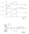
- Fig. 7 illustrates examples of electric pulses I1-I6 delivered to the electrodes E1 - E6 when a maximal number of ink droplets are to be ejected.
- Fig. 8 illustrates an example of an electric signal wave form relating to the two opposing electrodes E2 and E3 on the wall between channel C2 and channel C3.
- the temperature is measured by a temperature sensor and the voltage levels in the pulse wave forms are decreased with rising ink temperature.
- the voltage top value is set to 35 volts when the actuator temperature is 20°C.
- the voltage top value is set to its top value when the actuator temperature is 10°C.
- the voltage top level is herein referred to as the 100% voltage level.
- the temperature sensor is a thermistor.
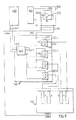
- Figure 9 is a block diagram of an embodiment of the invention, comprising an actuator control circuit 130, a power supply circuit 330, and an actuator 100.
- the power supply circuit 330 is coupled to a DC power supply 340.
- the power supply 340 may for example provide a substantially constant voltage of 40 volts.
- the power supply circuit 330 comprises a drive voltage controller 350, having an input 360 for a power demand signal and a power supply output 370 for delivering a drive voltage with a controlled voltage Vcc.
- the actuator control unit 130 comprises a power supply input 380 which is coupled to the output 370 for receiving a controlled drive voltage.
- the control unit 130 comprises a plurality of controllable current sources 320, each current source having a drive voltage input 400 which is coupled to the power supply input 380.
- N There may be provided N current sources, where N is an integer.
- Each current source 320:1, 320:2...320:N has an earth connection 410 and an actuator drive signal output 420.
- Each actuator drive signal output is coupled to the electrodes E of a corresponding channel wall in the actuator 100.
- Each current source 320 also comprises an input 430 for a current control signal.
- the current control signal input is coupled to a data conversion unit 440.
- the data conversion unit comprises an input 450 for receiving print data indicative of the text or picture to be printed.
- the input 450 is adapted to be connected to a data interface 460 via a databus 464.
- a plurality of electrical conductors 466 are provided to connect the control unit 130 with the data interface 460 and the power supply circuit 330.
- the data conversion unit 440 In response to print data received on the input 450 the data conversion unit 440 converts the print data into individual current control signals for each current source 320.
- the data conversion unit 440 comprises a control signal output 471 corresponding to each current source 320, and hence a current control signal for each channel in the actuator.
- the data conversion unit in co-operation with the controllable current sources 320 operates to generate drive currents on the outputs 420 such that the wave forms of the drive signals delivered to each actuator wall causes a controlled movement of each wall.
- the voltage amplitude of the drive current on each output 420 depends on the voltage on the power supply input 380.
- the actuator For the purpose of controlling the voltage level so as to compensate for the temperature dependency of the viscosity of the ink, the actuator includes a temperature sensor 470.
- the temperature sensor 470 provides a temperature signal which indicates the power demand for driving the actuator with optimum performance.
- the power demand signal input 360 of the power supply circuit is adapted to receive the signal from the sensor 470, or a demand signal derived from the sensor 470.
- the power demand signal delivered to the input 360 is derived from the signal from sensor 470 in combination with other performance affecting variables.
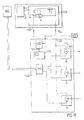
- Figure 10 is a block diagram of another embodiment of the ink jet printing arrangement. The embodiment according to Figure 10 differs from the embodiment according to Figure 9 in that the sensor 470 is coupled to an evaluation circuit 490, which operates to generate a voltage demand signal in dependence on sensed temperature. The output of the evaluation circuit 490 is coupled to the input 360 of the power supply circuit 350.
- the evaluation circuit 490 comprises an input 520 for receiving additional data relating to the performance affecting variables such as for example actuator efficiency and/or type of liquid. Such data includes for example data defining the temperature dependency of the liquid to be ejected by the actuator.
- the evaluation circuit 490 is, according to a preferred embodiment, integrated with the control unit 130.
- the additional data relating to performance of the actuator 100 are generated by an actuator status circuit 530.
- the actuator status circuit 530 also integrated in the control unit 130, includes a memory for storing data derived from measurements of the performance of the individual actuator control unit combination.
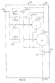
- the actuator control circuit 130 and the actuator 100 are arranged on a movable shuttle in a printer, while the data interface 460 and the drive voltage controller 350 are stationary parts in the printer.
- the set of conductors 466 is bendable so as to enable having one end attached to the firmly mounted power supply 330, and the other end connected to the movable shuttle which carries the control unit 130 and the actuator.
- the power supply 330 is separated in space from the control unit and from the actuator 100.
- the shuttle with the control unit and the actuator 100 moves during printing operations the separating distance between them changes. The separation in space leads to reduction or elimination of warmthing of the actuator 100 by thermal radiation from the variable voltage supply 330.
- the heat dissipation from the control unit to the actuator is reduced since the voltage drop in the control unit 130 is minimized.
- the signal sources 320 are designed for minimized voltage drop between the power input 380 and the outputs 420.
- the reduced power losses in the control unit thereby decreases the amount of heat generated in the immediate vicinity of the ink actuator, so as to reduce heat conduction from the control unit to the actuator.
- Fig 1 is a block diagram illustrating two of the controllable current signal sources 320:1 and 320:2 shown in Fig. 9, according to an embodiment of the invention.
- Fig. 11 also shows how two current sources 320:1 and 320:2 co-operate to provide a push-pull drive signal, as illustrated in Fig. 8, to an actuator wall 230 between channels CHk and CHk+1.
- each actuator wall is connected to two individually controlled current sources 320:k and 320:k+1.
- an actuator wall is connected so as to receive a push-pull signal from one pair of current sources 320:k and 320:k+1 whereas other walls receive push-pull signals from other pairs of current sources 320:j and 320:j+1; where k and j are positive integers, and j never equals k.
- a first actuator wall is coupled to receive a drive signal from a first pair of push-pull connected signal sources
- a second actuator wall is coupled to receive a drive signal from a second pair of push-pull connected signal sources, where the second pair is different from the first pair.
- a plurality of current signal sources 320 each such current source 320 being connected to at least one actuator wall.
- each current source 320 being connected to at least one actuator wall.
- control of the deflection of each wall is enabled by controlling the current delivered to it.
- one current source 320 for each actuator channel and the current through one wall is determined by the current sources connected to the channels bordering that wall.
- a current signal source 320 comprises a current source 500 receiving a drive voltage from the drive voltage input 400, and a control signal from the control signal input 430.
- the output of the current source 500 is coupled to a switch 515 for connecting the driver output 420 either to the output of the current source 500 or to ground 410.
- the switch 515 is also controlled by the signal from the control signal input 430.
- Fig. 11 illustrates a switch setting when current source 320:1 can drive a current via switch 515:1 through the wall between channels CH1 and CH2 and via switch 515:2 to ground.
- Figure 12 is a block diagram of a controllable drive signal source 320, according to another embodiment of the invention. Tests made by the inventors have shown that drop velocity depends on the slew rate of the drive signal shown in Fig. 8.
- the drive signal source is constructed with four output current sources 500:A, 500:B, 500:C, 500:D.
- Current source 500:B provides twice the current of current source 500:A.
- current source 500:C provides twice the current of current source 500:B
- current source 500:D provides twice the current of current source 500:C.
- a current ratio 1:2:4:8 is obtained.
- a switch unit 514 having switches 514:A, 514:B, 514:C and 514:D controls the activation of the individual current sources 500:A, 500:B, 500:C and 500:D, respectively.
- the current sources 500 include output devices, wherein the geometric area of an output device is directly proportional to the current it can provide, thereby making slew rate control possible.
- the output devices 500:A, 500:B, 500:C, 500:D are integrated circuit MOS transistors.
- the driver stage 320 is push-pull connected.
- the outputs of the current sources 500:A, 500:B, 500:C, 500:D are coupled to a switch 515 for connecting the driver output 420 to the outputs of the current sources 500:A, 500:B, 500:C, 500:D or to ground 410.
- a number of current sources (not shown) between the switch 515 and ground 410 so as to enable control of the negative slope of the pulse signal delivered on output 420.
- These current sources are pulling current sources of values corresponding to the pushing current sources 500:A, 500:B, 500:C, 500:D, and these current sources are also controlled by the switch means 514.
- a separate switch for controlling the pulling current sources.
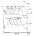
- FIG 13 is a schematic of an embodiment of a controllable drive signal source 320.
- Each of the N actuator channels is coupled to a non-inverting drive signal source 320.
- the actuator load appears as a large capacitor and parallel resistor strung between each neighbouring driver output.
- the dielectric of these capacitors is formed by the piezoelectric material in the wall 230 (Fig. 2).
- the driver 320:k drives the output 420:k to the positive rail, whilst the outputs 420:k-1 and 420:k+1 of the neighbouring channels (C k-1 and C k+1 ) are held at the negative rail. This charges the two capacitors of the walls of channel C k .
- a reverse polarity pulse is applied, see Figs. 5, 7 and 8, reversing the charge polarity of the wall capacitor. Again, this deflects the channel walls so as to contract the channel (Fig. 5C). Finally, during a recovery stage the potential across the wall 230 is restored to zero as the wall capacitance is discharged to their initial state.
- a two output bipolar NPN-transistors 540 and 550 forming the switch 515.
- a number of MOS transistors form the current sources 500:A, 500:B, 500:C and 500:D, as described above, for driving the output 420 to the positive.
- a number of NPN-transistors 560A, 560B, 560C, and 560D act as current sources 560 for driving the output 420 to the negative rail.
- the output drive capacity of the output bipolar NPN-transistors 540 and 550 is determined by the MOS transistors 500:A, 500:B, 500:C , 500:D and by the NPN-transistors 560A, 560B, 560C, and 560D,
- the MOS transistors 500 and the NPN-transistors 560 limit the available base current for the NPN-transistors 540 and 550, thereby determining the slew rate when switching these devices in a controlled manner.
- the output state is determined by control signals GA, GB, GC, GD, BA, BB, BC and BD which are related to the signal on control signal input 430, as described above. With reference to Fig. 13 and Fig.
- a switch 514 e.g. in the form of a fusible link memory, may be provided between the input 430 and the terminals GA, GB, GC, GD, BA, BB, BC and BD.
Landscapes
- Particle Formation And Scattering Control In Inkjet Printers (AREA)
- Ink Jet (AREA)
Applications Claiming Priority (5)
| Application Number | Priority Date | Filing Date | Title |
|---|---|---|---|
| SE9703983 | 1997-10-30 | ||
| SE9703983A SE9703983L (sv) | 1997-10-30 | 1997-10-30 | Bläckstråleskrivare |
| SE9802142A SE9802142L (sv) | 1998-06-16 | 1998-06-16 | Bläckstråleskrivare |
| SE9802142 | 1998-06-16 | ||
| PCT/SE1998/001962 WO1999022938A1 (en) | 1997-10-30 | 1998-10-30 | Ink jet printer |
Publications (2)
| Publication Number | Publication Date |
|---|---|
| EP1027217A1 EP1027217A1 (en) | 2000-08-16 |
| EP1027217B1 true EP1027217B1 (en) | 2001-12-19 |
Family
ID=26663117
Family Applications (2)
| Application Number | Title | Priority Date | Filing Date |
|---|---|---|---|
| EP98953127A Expired - Lifetime EP1027218B1 (en) | 1997-10-30 | 1998-10-30 | Ink jet printer |
| EP98953123A Expired - Lifetime EP1027217B1 (en) | 1997-10-30 | 1998-10-30 | Ink jet printer |
Family Applications Before (1)
| Application Number | Title | Priority Date | Filing Date |
|---|---|---|---|
| EP98953127A Expired - Lifetime EP1027218B1 (en) | 1997-10-30 | 1998-10-30 | Ink jet printer |
Country Status (8)
| Country | Link |
|---|---|
| US (2) | US6312080B1 (zh) |
| EP (2) | EP1027218B1 (zh) |
| JP (2) | JP2001521841A (zh) |
| CN (1) | CN1196587C (zh) |
| AU (2) | AU1058099A (zh) |
| CA (2) | CA2308035A1 (zh) |
| DE (2) | DE69818292T2 (zh) |
| WO (2) | WO1999022939A1 (zh) |
Families Citing this family (16)
| Publication number | Priority date | Publication date | Assignee | Title |
|---|---|---|---|---|
| IL149613A0 (en) * | 1999-11-17 | 2002-11-10 | Xaar Technology Ltd | Droplet deposition apparatus |
| US20040085374A1 (en) * | 2002-10-30 | 2004-05-06 | Xerox Corporation | Ink jet apparatus |
| US6739690B1 (en) * | 2003-02-11 | 2004-05-25 | Xerox Corporation | Ink jet apparatus |
| US7021733B2 (en) * | 2003-11-05 | 2006-04-04 | Xerox Corporation | Ink jet apparatus |
| US7055939B2 (en) * | 2003-11-20 | 2006-06-06 | Xerox Corporation | Drop generator |
| US7227756B2 (en) * | 2004-05-27 | 2007-06-05 | Lexmark International, Inc. | Power supply keying arrangement for use with an electrical apparatus |
| US7631953B2 (en) * | 2006-03-31 | 2009-12-15 | Lexmark International, Inc. | Micro-fluid ejection apparatus signal communication devices and methods |
| JP2009537355A (ja) * | 2006-05-24 | 2009-10-29 | オセ−テクノロジーズ・ベー・ヴエー | インクジェットプリンタを使用して画像を得る方法およびその方法の実施に適したプリンタ |
| WO2010052132A1 (en) * | 2008-11-05 | 2010-05-14 | Oce-Technologies B.V. | A driver circuit for driving a print head of an inkjet printer |
| JP5689651B2 (ja) * | 2010-11-09 | 2015-03-25 | エスアイアイ・プリンテック株式会社 | 液体噴射ヘッド、液体噴射装置及び液体噴射ヘッドの駆動方法 |
| WO2013162539A1 (en) * | 2012-04-25 | 2013-10-31 | Hewlett-Packard Development Company, L.P. | Adaptive level shifter for print nozzle amplifier |
| GB2540114B (en) * | 2015-03-20 | 2019-11-20 | Archipelago Tech Group Ltd | Method, system, and device for supplying electrical energy through electrical conductors adjacent to electrolyte solution environments |
| JP6811552B2 (ja) * | 2015-11-26 | 2021-01-13 | 東芝テック株式会社 | インクジェットヘッド、及びインクジェット記録装置 |
| US10569542B2 (en) * | 2016-08-16 | 2020-02-25 | Zebra Technologies Corporation | Printhead pin configurations |
| US9975330B1 (en) | 2017-04-17 | 2018-05-22 | Xerox Corporation | System and method for generation of non-firing electrical signals for operation of ejectors in inkjet printheads |
| JP6999317B2 (ja) * | 2017-07-21 | 2022-01-18 | 東芝テック株式会社 | インクジェットヘッド及びインクジェットプリンタ |
Citations (1)
| Publication number | Priority date | Publication date | Assignee | Title |
|---|---|---|---|---|
| US6531675B2 (en) * | 2001-01-31 | 2003-03-11 | Unova Ip Corp. | Laser welding method and apparatus |
Family Cites Families (10)
| Publication number | Priority date | Publication date | Assignee | Title |
|---|---|---|---|---|
| DE2903339B2 (de) | 1979-01-29 | 1980-11-13 | Siemens Ag, 1000 Berlin Und 8000 Muenchen | Schaltungsanordnung zur temperaturabhängigen Spannungsregelung für piezoelektrische Schreibdüsen in Tintenmosaikschreibeinrichtungen |
| US4689694A (en) * | 1983-01-12 | 1987-08-25 | Canon Kabushiki Kaisha | Image recording apparatus utilizing linearly arranged recording elements |
| GB8824014D0 (en) | 1988-10-13 | 1988-11-23 | Am Int | High density multi-channel array electrically pulsed droplet deposition apparatus |
| US5461403A (en) | 1991-08-16 | 1995-10-24 | Compaq Computer Corporation | Droplet volume modulation techniques for ink jet printheads |
| US5502468A (en) | 1992-12-28 | 1996-03-26 | Tektronix, Inc. | Ink jet print head drive with normalization |
| JP3143549B2 (ja) | 1993-09-08 | 2001-03-07 | キヤノン株式会社 | 熱記録ヘッド用基体、該基体を用いたインクジェット記録ヘッド、インクジェットカートリッジ、インクジェット記録装置、及び記録ヘッドの駆動方法 |
| JP3503656B2 (ja) | 1993-10-05 | 2004-03-08 | セイコーエプソン株式会社 | インクジェットヘッドの駆動装置 |
| DE9401249U1 (de) | 1993-12-28 | 1994-06-30 | Mts Produkte Gmbh | Flüssigkeitsfilter |
| JPH09216361A (ja) * | 1995-12-05 | 1997-08-19 | Tec Corp | インクジェットプリンタのヘッド駆動装置 |
| DE69736991T2 (de) * | 1996-01-29 | 2007-07-12 | Seiko Epson Corp. | Tintenstrahlaufzeichnungskopf |
-
1998
- 1998-10-30 US US09/530,032 patent/US6312080B1/en not_active Expired - Fee Related
- 1998-10-30 DE DE69818292T patent/DE69818292T2/de not_active Expired - Fee Related
- 1998-10-30 EP EP98953127A patent/EP1027218B1/en not_active Expired - Lifetime
- 1998-10-30 US US09/530,148 patent/US6450624B1/en not_active Expired - Fee Related
- 1998-10-30 CN CNB988108623A patent/CN1196587C/zh not_active Expired - Fee Related
- 1998-10-30 DE DE69803092T patent/DE69803092T2/de not_active Expired - Fee Related
- 1998-10-30 WO PCT/SE1998/001972 patent/WO1999022939A1/en active IP Right Grant
- 1998-10-30 CA CA002308035A patent/CA2308035A1/en not_active Abandoned
- 1998-10-30 JP JP2000518840A patent/JP2001521841A/ja active Pending
- 1998-10-30 WO PCT/SE1998/001962 patent/WO1999022938A1/en active IP Right Grant
- 1998-10-30 AU AU10580/99A patent/AU1058099A/en not_active Abandoned
- 1998-10-30 JP JP2000518841A patent/JP2001521842A/ja active Pending
- 1998-10-30 CA CA002309041A patent/CA2309041A1/en not_active Abandoned
- 1998-10-30 AU AU10577/99A patent/AU1057799A/en not_active Abandoned
- 1998-10-30 EP EP98953123A patent/EP1027217B1/en not_active Expired - Lifetime
Patent Citations (1)
| Publication number | Priority date | Publication date | Assignee | Title |
|---|---|---|---|---|
| US6531675B2 (en) * | 2001-01-31 | 2003-03-11 | Unova Ip Corp. | Laser welding method and apparatus |
Also Published As
| Publication number | Publication date |
|---|---|
| EP1027218A1 (en) | 2000-08-16 |
| EP1027218B1 (en) | 2003-09-17 |
| CN1196587C (zh) | 2005-04-13 |
| AU1058099A (en) | 1999-05-24 |
| US6312080B1 (en) | 2001-11-06 |
| CN1278212A (zh) | 2000-12-27 |
| WO1999022939A1 (en) | 1999-05-14 |
| JP2001521842A (ja) | 2001-11-13 |
| DE69818292D1 (de) | 2003-10-23 |
| DE69818292T2 (de) | 2004-06-03 |
| CA2308035A1 (en) | 1999-05-14 |
| CA2309041A1 (en) | 1999-05-14 |
| AU1057799A (en) | 1999-05-24 |
| WO1999022938A1 (en) | 1999-05-14 |
| DE69803092T2 (de) | 2002-07-18 |
| DE69803092D1 (de) | 2002-01-31 |
| US6450624B1 (en) | 2002-09-17 |
| EP1027217A1 (en) | 2000-08-16 |
| JP2001521841A (ja) | 2001-11-13 |
Similar Documents
| Publication | Publication Date | Title |
|---|---|---|
| EP1027217B1 (en) | Ink jet printer | |
| TW293226B (zh) | ||
| US4521786A (en) | Programmable driver/controller for ink jet printheads | |
| US5359350A (en) | Method of driving ink jet printing head | |
| US4126867A (en) | Ink jet printer driving circuit | |
| US7651203B2 (en) | Inkjet recording device, ejecting device provided therein, and method of calibrating ejection characteristic for droplet | |
| EP1936343B1 (en) | Temperature detector and recording apparatus including the same | |
| CN110091600B (zh) | 液体喷出装置 | |
| US7852127B2 (en) | Driving circuit for capacitive load and fluid injecting device | |
| US7880515B2 (en) | Driving circuit for capacitive load and fluid injecting device | |
| US6247776B1 (en) | Ink jet recording apparatus for adjusting the weight of ink droplets | |
| EP3695969B1 (en) | Driving circuit, liquid discharge apparatus, and driving method | |
| JPH07125195A (ja) | インクジェットヘッドの駆動方法 | |
| EP1230090A1 (en) | Droplet deposition apparatus | |
| US4566017A (en) | Method and transducer for increasing inking resolution in an ink-mosaic recording device | |
| CN113825643B (zh) | 喷墨记录装置、喷墨记录装置的调整方法以及喷墨记录装置的控制方法 | |
| EP1322475B1 (en) | Droplet deposition apparatus | |
| JP3531366B2 (ja) | インクジェット記録装置 | |
| JPH09123442A (ja) | インクジェット記録ヘッドの駆動装置 | |
| JPH08295015A (ja) | インクジェットヘッドの温度制御方法 | |
| JP7400304B2 (ja) | 液体吐出ヘッドおよび液体吐出装置 | |
| US10252522B2 (en) | Liquid ejecting apparatus | |
| JPH11342608A (ja) | インクジェット記録装置 | |
| JP2001301157A (ja) | インクジェットヘッドの駆動方法及びインクジェット記録装置 | |
| JPH09277526A (ja) | 圧電素子駆動回路 |
Legal Events
| Date | Code | Title | Description |
|---|---|---|---|
| PUAI | Public reference made under article 153(3) epc to a published international application that has entered the european phase |
Free format text: ORIGINAL CODE: 0009012 |
|
| 17P | Request for examination filed |
Effective date: 20000517 |
|
| AK | Designated contracting states |
Kind code of ref document: A1 Designated state(s): DE FR GB SE |
|
| GRAG | Despatch of communication of intention to grant |
Free format text: ORIGINAL CODE: EPIDOS AGRA |
|
| RIN1 | Information on inventor provided before grant (corrected) |
Inventor name: BOSTROEM, CHRISTER Inventor name: DE ROOS, MIKE |
|
| 17Q | First examination report despatched |
Effective date: 20001205 |
|
| GRAG | Despatch of communication of intention to grant |
Free format text: ORIGINAL CODE: EPIDOS AGRA |
|
| GRAG | Despatch of communication of intention to grant |
Free format text: ORIGINAL CODE: EPIDOS AGRA |
|
| GRAH | Despatch of communication of intention to grant a patent |
Free format text: ORIGINAL CODE: EPIDOS IGRA |
|
| GRAH | Despatch of communication of intention to grant a patent |
Free format text: ORIGINAL CODE: EPIDOS IGRA |
|
| GRAA | (expected) grant |
Free format text: ORIGINAL CODE: 0009210 |
|
| AK | Designated contracting states |
Kind code of ref document: B1 Designated state(s): DE FR GB SE |
|
| REG | Reference to a national code |
Ref country code: GB Ref legal event code: IF02 |
|
| REF | Corresponds to: |
Ref document number: 69803092 Country of ref document: DE Date of ref document: 20020131 |
|
| ET | Fr: translation filed | ||
| PGFP | Annual fee paid to national office [announced via postgrant information from national office to epo] |
Ref country code: SE Payment date: 20021004 Year of fee payment: 5 |
|
| PLBE | No opposition filed within time limit |
Free format text: ORIGINAL CODE: 0009261 |
|
| STAA | Information on the status of an ep patent application or granted ep patent |
Free format text: STATUS: NO OPPOSITION FILED WITHIN TIME LIMIT |
|
| 26N | No opposition filed | ||
| PG25 | Lapsed in a contracting state [announced via postgrant information from national office to epo] |
Ref country code: SE Free format text: LAPSE BECAUSE OF NON-PAYMENT OF DUE FEES Effective date: 20031031 |
|
| EUG | Se: european patent has lapsed | ||
| PGFP | Annual fee paid to national office [announced via postgrant information from national office to epo] |
Ref country code: DE Payment date: 20071025 Year of fee payment: 10 |
|
| PGFP | Annual fee paid to national office [announced via postgrant information from national office to epo] |
Ref country code: GB Payment date: 20071024 Year of fee payment: 10 Ref country code: FR Payment date: 20071009 Year of fee payment: 10 |
|
| GBPC | Gb: european patent ceased through non-payment of renewal fee |
Effective date: 20081030 |
|
| REG | Reference to a national code |
Ref country code: FR Ref legal event code: ST Effective date: 20090630 |
|
| PG25 | Lapsed in a contracting state [announced via postgrant information from national office to epo] |
Ref country code: DE Free format text: LAPSE BECAUSE OF NON-PAYMENT OF DUE FEES Effective date: 20090501 |
|
| PG25 | Lapsed in a contracting state [announced via postgrant information from national office to epo] |
Ref country code: FR Free format text: LAPSE BECAUSE OF NON-PAYMENT OF DUE FEES Effective date: 20081031 |
|
| PG25 | Lapsed in a contracting state [announced via postgrant information from national office to epo] |
Ref country code: GB Free format text: LAPSE BECAUSE OF NON-PAYMENT OF DUE FEES Effective date: 20081030 |