EP1024505A1 - Chip electronic component and manufacturing method thereof - Google Patents
Chip electronic component and manufacturing method thereof Download PDFInfo
- Publication number
- EP1024505A1 EP1024505A1 EP00101005A EP00101005A EP1024505A1 EP 1024505 A1 EP1024505 A1 EP 1024505A1 EP 00101005 A EP00101005 A EP 00101005A EP 00101005 A EP00101005 A EP 00101005A EP 1024505 A1 EP1024505 A1 EP 1024505A1
- Authority
- EP
- European Patent Office
- Prior art keywords
- coating material
- electronic component
- resin coating
- chip
- chip electronic
- Prior art date
- Legal status (The legal status is an assumption and is not a legal conclusion. Google has not performed a legal analysis and makes no representation as to the accuracy of the status listed.)
- Granted
Links
Images



Classifications
-
- H—ELECTRICITY
- H01—ELECTRIC ELEMENTS
- H01F—MAGNETS; INDUCTANCES; TRANSFORMERS; SELECTION OF MATERIALS FOR THEIR MAGNETIC PROPERTIES
- H01F17/00—Fixed inductances of the signal type
- H01F17/04—Fixed inductances of the signal type with magnetic core
- H01F17/045—Fixed inductances of the signal type with magnetic core with core of cylindric geometry and coil wound along its longitudinal axis, i.e. rod or drum core
-
- H—ELECTRICITY
- H01—ELECTRIC ELEMENTS
- H01F—MAGNETS; INDUCTANCES; TRANSFORMERS; SELECTION OF MATERIALS FOR THEIR MAGNETIC PROPERTIES
- H01F41/00—Apparatus or processes specially adapted for manufacturing or assembling magnets, inductances or transformers; Apparatus or processes specially adapted for manufacturing materials characterised by their magnetic properties
- H01F41/02—Apparatus or processes specially adapted for manufacturing or assembling magnets, inductances or transformers; Apparatus or processes specially adapted for manufacturing materials characterised by their magnetic properties for manufacturing cores, coils, or magnets
- H01F41/04—Apparatus or processes specially adapted for manufacturing or assembling magnets, inductances or transformers; Apparatus or processes specially adapted for manufacturing materials characterised by their magnetic properties for manufacturing cores, coils, or magnets for manufacturing coils
- H01F41/12—Insulating of windings
- H01F41/127—Encapsulating or impregnating
-
- Y—GENERAL TAGGING OF NEW TECHNOLOGICAL DEVELOPMENTS; GENERAL TAGGING OF CROSS-SECTIONAL TECHNOLOGIES SPANNING OVER SEVERAL SECTIONS OF THE IPC; TECHNICAL SUBJECTS COVERED BY FORMER USPC CROSS-REFERENCE ART COLLECTIONS [XRACs] AND DIGESTS
- Y10—TECHNICAL SUBJECTS COVERED BY FORMER USPC
- Y10T—TECHNICAL SUBJECTS COVERED BY FORMER US CLASSIFICATION
- Y10T29/00—Metal working
- Y10T29/49—Method of mechanical manufacture
- Y10T29/49002—Electrical device making
- Y10T29/4902—Electromagnet, transformer or inductor
-
- Y—GENERAL TAGGING OF NEW TECHNOLOGICAL DEVELOPMENTS; GENERAL TAGGING OF CROSS-SECTIONAL TECHNOLOGIES SPANNING OVER SEVERAL SECTIONS OF THE IPC; TECHNICAL SUBJECTS COVERED BY FORMER USPC CROSS-REFERENCE ART COLLECTIONS [XRACs] AND DIGESTS
- Y10—TECHNICAL SUBJECTS COVERED BY FORMER USPC
- Y10T—TECHNICAL SUBJECTS COVERED BY FORMER US CLASSIFICATION
- Y10T29/00—Metal working
- Y10T29/49—Method of mechanical manufacture
- Y10T29/49002—Electrical device making
- Y10T29/4902—Electromagnet, transformer or inductor
- Y10T29/49073—Electromagnet, transformer or inductor by assembling coil and core
Definitions
- a chip inductor in which a coil is wound around the core portion of a core
- a spiral inductor having a structure in which a coil is wound around the core portion of a double enveloping core (barbell-like core) and soldered to external electrodes made of metallic plates provided on flange portions on both ends of the coil, respectively.
- the inductor of this type it is necessary to take account of reliability such as a possible damage to be made while mounting steps are conducted or the inductor is being handled, due to the exposed coil.
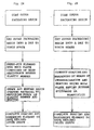
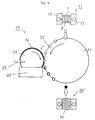
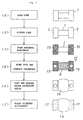
- a manufacturing method comprising coating a resin coating material 14 serving as an outer packaging material stored in a coating material pan 23 on the periphery of a chip inductor element 11 having the core portion 1 of a double enveloping core 7 put crosswise and the end portions of the coil 8 soldered and connected to directly bonded external electrodes 15 provided on the flange portions on the both ends of the core portion 1 by means of a coater 27 by means of the rotation of the coating disk 24, while the element is held by a product chuck 22 of a rotating drum disk 21 and rotated, heating and hardening the resin coating material 14 thus coated and finally plating the external electrodes.
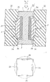
- the chip is put into a mold plate of a desired outer shape having stiffness and heated while being pressurized, whereby the chip can be shaped and hardened to have a desired outer shape.
- the chip shape is a combination of planes, i.e., the chip is a chip electronic component of rectangular shape (typically rectangular parallelopiped shape)
- the shaping can be easily realized by inserting the chip into metallic mold plates with one of the plates opened, pushing the chip against a push plate fitted into the opening surface and pressurizing and heating the chip.
- the chip electronic component and the chip electronic component manufacturing method according to the present invention has the following (1) to (10) advantages.
Landscapes
- Engineering & Computer Science (AREA)
- Power Engineering (AREA)
- Manufacturing & Machinery (AREA)
- Microelectronics & Electronic Packaging (AREA)
- Coils Or Transformers For Communication (AREA)
- Manufacturing Cores, Coils, And Magnets (AREA)
- Insulating Of Coils (AREA)
Abstract
Description
- 7
- double enveloping core
- 8
- coil
- 14
- resin coating material
- 14'
- magnetic powder containing resin
- 10, 20, 30
- chip inductor
- 20'
- chip inductor element
- 27
- coater
- 31
- component storage section
- 32
- heat resistance rubber elastic member
- 33
- mold plate
- t1
- thickness of circumferential thin portion of outer packaging material
- t2
- thickness of circumferential thick portion of outer packaging material
Claims (10)
- A chip electronic component having an outer packaging material annually coating the periphery of an element, characterized in thatsaid element has flanges on longitudinal both ends, respectively; anda dimensional ratio (t2/t1) of a thickness (t1) of a circumferential thin portion of the outer packaging material formed on the outer periphery of the element to a thickness (t2) of a thick portion of the outer packaging material is not less than 2 so that at least part of the respective flanges are exposed.
- A chip electronic component according to claim 1, characterized in that the outer packaging material is magnetic powder containing resin containing magnetic powder of 75 % by weight or more.
- A chip electronic component according to claim 2, characterized in that a largest particle size of the magnetic powder contained in the outer packaging material is not more than the thickness (t1) of the circumferential thin portion of the outer packaging material.
- A chip electronic component manufacturing method comprising a step of coating, as an outer packaging material, a resin coating material on the periphery of an element of the electronic component and a step of heating and hardening said resin coating material, said method characterized in thatthe chip electronic component coated with said resin coating material is press-fitted into a component storage section having a desired outer shape included in a heat resistance rubber elastic member so as to elastically deform said component storage section and the chip electronic component together with said heat resistance rubber elastic member, thereby shaping and hardening said resin coating material into a desired shape.
- A chip electronic component manufacturing method comprising a step of coating a resin coating material on the periphery of an element of the chip electronic component except for an external electrode disposed region, and a step of heating and hardening said resin coating material, the method characterized by comprising a step of press-fitting the chip electronic component coated with said resin coating material into a component storage section having a desired outer shape in a mold plate comprised of a heat resistance rubber elastic member including said component storage section so as to elastically deform said component storage section while said resin coating material coating said electronic component is in a dry to touch state, and heating said electronic component together with said mold plate to thereby harden said resin coating material.
- A chip electronic component manufacturing method comprising a step of coating a resin coating material on the periphery of a coil of a chip inductor element having external electrodes disposed at flanged portions on both ends of a double enveloping core, with the coil wound around a core portion of the double enveloping core and end portions of the coil thermo-compressed to said external electrodes, and a step of heating and hardening said resin coating material, the method characterized by comprising a step of press-fitting said chip inductor element into a component storage section having a desired chip outer shape in a mold plate comprised of a heat resistance rubber elastic member including said storage section while said resin coating material coating said chip inductor element is in a dry to touch state, and heating said chip inductor element together with said mold plate to thereby harden said resin coating material.
- A chip electronic component manufacturing method according to claim 6, characterized in that the outer shape of said component storage section having the mold plate shape consists of a plurality of planes or of a combination of a plurality of planes and a round ridgeline.
- A chip electronic component manufacturing method according to claim 6 or 7, characterized in that run-off portions to which excessive resin coating material is extruded when heating the resin coating material are provided at the flanged portions on the both ends of the double enveloping core of said chip electronic component or portions of the component storage section corresponding to the flanged portions.
- A chip electronic component manufacturing method comprising a step of coating a resin coating material on the periphery of an element of the chip electronic component except for an external electrode disposed region, and a step of heating and hardening said resin coating material, the method characterized by comprising a step of coating said electronic component element with the resin coating material, and a step of pressurizing and heating said electronic component element by a mold plate of a desired shape having stiffness while said resin coating material is in a dry to touch state, thereby shaping and hardening said resin coating material into a desired outer shape.
- A chip electronic component manufacturing method comprising a step of coating a resin coating material on the periphery of an element of a chip electronic component element except for an external electrode disposed region, and a step of heating and hardening said resin coating material, the method characterized by comprising a step of coating said electronic component element with the resin coating material, and a step of pressurizing and heating said resin coating material using an elastic mold plate of a desired shape while said resin coating material is in a dry to touch state, thereby shaping and hardening said resin coating material into a desired outer shape.
Applications Claiming Priority (4)
| Application Number | Priority Date | Filing Date | Title |
|---|---|---|---|
| JP2026599 | 1999-01-28 | ||
| JP2026599 | 1999-01-28 | ||
| JP36224599 | 1999-12-21 | ||
| JP36224599A JP4039779B2 (en) | 1999-01-28 | 1999-12-21 | Manufacturing method of chip-shaped electronic component |
Publications (2)
| Publication Number | Publication Date |
|---|---|
| EP1024505A1 true EP1024505A1 (en) | 2000-08-02 |
| EP1024505B1 EP1024505B1 (en) | 2004-06-09 |
Family
ID=26357172
Family Applications (1)
| Application Number | Title | Priority Date | Filing Date |
|---|---|---|---|
| EP00101005A Expired - Lifetime EP1024505B1 (en) | 1999-01-28 | 2000-01-19 | Chip electronic component and manufacturing method thereof |
Country Status (4)
| Country | Link |
|---|---|
| US (2) | US6393691B1 (en) |
| EP (1) | EP1024505B1 (en) |
| JP (1) | JP4039779B2 (en) |
| DE (1) | DE60011317T2 (en) |
Cited By (2)
| Publication number | Priority date | Publication date | Assignee | Title |
|---|---|---|---|---|
| DE20300713U1 (en) | 2003-01-16 | 2003-03-27 | Neosid Pemetzrieder GmbH & Co KG, 58553 Halver | Miniature inductive component for SMD assembly |
| CN112164572A (en) * | 2020-09-01 | 2021-01-01 | 安徽省瀚海新材料股份有限公司 | Compression molding process of neodymium iron boron product |
Families Citing this family (32)
| Publication number | Priority date | Publication date | Assignee | Title |
|---|---|---|---|---|
| JP4039779B2 (en) * | 1999-01-28 | 2008-01-30 | 太陽誘電株式会社 | Manufacturing method of chip-shaped electronic component |
| JP3591413B2 (en) * | 2000-03-14 | 2004-11-17 | 株式会社村田製作所 | Inductor and manufacturing method thereof |
| US6918173B2 (en) * | 2000-07-31 | 2005-07-19 | Ceratech Corporation | Method for fabricating surface mountable chip inductor |
| US6864774B2 (en) * | 2000-10-19 | 2005-03-08 | Matsushita Electric Industrial Co., Ltd. | Inductance component and method of manufacturing the same |
| JP3582477B2 (en) * | 2000-11-01 | 2004-10-27 | 株式会社村田製作所 | Electronic component and method of manufacturing the same |
| JP2003115403A (en) * | 2001-10-03 | 2003-04-18 | Matsushita Electric Ind Co Ltd | Manufacturing method of electronic components |
| AU2003201729A1 (en) * | 2002-02-28 | 2003-09-09 | Koninklijke Philips Electronics N.V. | Transformer |
| US6873241B1 (en) * | 2003-03-24 | 2005-03-29 | Robert O. Sanchez | High frequency transformers and high Q factor inductors formed using epoxy-based magnetic polymer materials |
| US7170381B2 (en) * | 2003-07-09 | 2007-01-30 | Power Integrations, Inc. | Method and apparatus for transferring energy in a power converter circuit |
| US7088211B2 (en) * | 2003-07-15 | 2006-08-08 | Astec International Limited | Space saving surface-mounted inductors |
| JP4581353B2 (en) * | 2003-08-21 | 2010-11-17 | 株式会社村田製作所 | Winding coil parts |
| JP2005210055A (en) * | 2003-12-22 | 2005-08-04 | Taiyo Yuden Co Ltd | Surface mount coil part and manufacturing method of the same |
| JP2006100700A (en) * | 2004-09-30 | 2006-04-13 | Chuki Seiki Kk | Noise rejection device |
| JP2006100697A (en) * | 2004-09-30 | 2006-04-13 | Chuki Seiki Kk | Noise rejection device |
| US7518463B2 (en) * | 2004-12-23 | 2009-04-14 | Agilent Technologies, Inc. | Circuit assembly with conical inductor |
| JP4290160B2 (en) * | 2005-12-22 | 2009-07-01 | Tdk株式会社 | Coil component and method for manufacturing coil component |
| JP4535083B2 (en) * | 2007-04-10 | 2010-09-01 | Tdk株式会社 | Coil parts |
| TWM332922U (en) * | 2007-10-11 | 2008-05-21 | Darfon Electronics Corp | Inductance |
| US20100134233A1 (en) * | 2008-11-28 | 2010-06-03 | Shih-Jen Wang | Inductor and method for making the same |
| WO2011064863A1 (en) * | 2009-11-26 | 2011-06-03 | トヨタ自動車株式会社 | Reactor-securing structure |
| JP2011165696A (en) * | 2010-02-04 | 2011-08-25 | Murata Mfg Co Ltd | Method of manufacturing winding coil component |
| JP5561536B2 (en) * | 2010-06-17 | 2014-07-30 | 住友電気工業株式会社 | Reactor and converter |
| EP2530686B1 (en) * | 2011-06-01 | 2014-08-06 | ABB Research Ltd. | Pressing of transformer windings during active part drying |
| US9141157B2 (en) * | 2011-10-13 | 2015-09-22 | Texas Instruments Incorporated | Molded power supply system having a thermally insulated component |
| KR20140082355A (en) * | 2012-12-24 | 2014-07-02 | 삼성전기주식회사 | Inductor and manufacturing method thereof |
| JP6372421B2 (en) | 2015-06-02 | 2018-08-15 | 株式会社村田製作所 | Method for manufacturing wound coil |
| TWI609391B (en) * | 2016-02-09 | 2017-12-21 | 村田製作所股份有限公司 | Winding coil manufacturing method |
| US11335497B2 (en) * | 2016-08-19 | 2022-05-17 | Meggit Aerospace Limited | Electromagnetic coils and methods of making same |
| JP6959062B2 (en) * | 2017-08-02 | 2021-11-02 | 太陽誘電株式会社 | Coil parts |
| JP6769450B2 (en) * | 2018-01-30 | 2020-10-14 | 株式会社村田製作所 | Inductor parts |
| US20200303114A1 (en) * | 2019-03-22 | 2020-09-24 | Cyntec Co., Ltd. | Inductor array in a single package |
| JP7835596B2 (en) * | 2022-03-29 | 2026-03-25 | 太陽誘電株式会社 | Manufacturing method for coil components |
Citations (4)
| Publication number | Priority date | Publication date | Assignee | Title |
|---|---|---|---|---|
| DE3042433A1 (en) * | 1980-11-11 | 1982-07-01 | Draloric Electronic GmbH, 8500 Nürnberg | Inductive component for printed circuit mounting - has ends of wire coil wound round cylindrical central portion, and electrically coupled to both metal films on end blocks |
| JPH02301115A (en) * | 1989-05-15 | 1990-12-13 | Nec Corp | Chip type solid electrolytic capacitor |
| JPH08255806A (en) * | 1995-03-17 | 1996-10-01 | Toshiba Corp | Method for manufacturing resin-sealed semiconductor device |
| EP0845792A2 (en) * | 1996-11-29 | 1998-06-03 | Taiyo Yuden Co., Ltd. | Wire wound electronic component and method of manufacturing the same |
Family Cites Families (12)
| Publication number | Priority date | Publication date | Assignee | Title |
|---|---|---|---|---|
| JPH08180731A (en) * | 1994-12-26 | 1996-07-12 | Murata Mfg Co Ltd | Conductive thick film composition, thick film electrode, ceramic electronic component, and multilayer ceramic capacitor |
| CN1075661C (en) * | 1995-06-08 | 2001-11-28 | 松下电器产业株式会社 | Chip coil |
| TW342506B (en) * | 1996-10-11 | 1998-10-11 | Matsushita Electric Industrial Co Ltd | Inductance device and wireless terminal equipment |
| WO1998044520A1 (en) * | 1997-03-28 | 1998-10-08 | Matsushita Electric Industrial Co., Ltd. | Chip inductor and method for manufacturing the same |
| US6194248B1 (en) * | 1997-09-02 | 2001-02-27 | Murata Manufacturing Co., Ltd. | Chip electronic part |
| JP3317213B2 (en) * | 1997-10-06 | 2002-08-26 | 株式会社村田製作所 | Wound type chip inductor |
| JP3352950B2 (en) * | 1998-07-13 | 2002-12-03 | 太陽誘電株式会社 | Chip inductor |
| US6157283A (en) * | 1998-11-24 | 2000-12-05 | Taiyo Yuden Co., Ltd. | Surface-mounting-type coil component |
| JP4039779B2 (en) * | 1999-01-28 | 2008-01-30 | 太陽誘電株式会社 | Manufacturing method of chip-shaped electronic component |
| US6298544B1 (en) * | 1999-03-24 | 2001-10-09 | Inpaq Technology Co., Ltd. | Method of fabricating a high frequency thin film coil element |
| CN1178232C (en) * | 1999-04-26 | 2004-12-01 | 松下电器产业株式会社 | Electronic components and wireless terminal devices |
| TW469456B (en) * | 1999-06-30 | 2001-12-21 | Murata Manufacturing Co | LC component |
-
1999
- 1999-12-21 JP JP36224599A patent/JP4039779B2/en not_active Expired - Fee Related
-
2000
- 2000-01-19 EP EP00101005A patent/EP1024505B1/en not_active Expired - Lifetime
- 2000-01-19 DE DE60011317T patent/DE60011317T2/en not_active Expired - Lifetime
- 2000-01-27 US US09/492,856 patent/US6393691B1/en not_active Expired - Fee Related
-
2001
- 2001-12-03 US US10/012,103 patent/US6856229B2/en not_active Expired - Lifetime
Patent Citations (4)
| Publication number | Priority date | Publication date | Assignee | Title |
|---|---|---|---|---|
| DE3042433A1 (en) * | 1980-11-11 | 1982-07-01 | Draloric Electronic GmbH, 8500 Nürnberg | Inductive component for printed circuit mounting - has ends of wire coil wound round cylindrical central portion, and electrically coupled to both metal films on end blocks |
| JPH02301115A (en) * | 1989-05-15 | 1990-12-13 | Nec Corp | Chip type solid electrolytic capacitor |
| JPH08255806A (en) * | 1995-03-17 | 1996-10-01 | Toshiba Corp | Method for manufacturing resin-sealed semiconductor device |
| EP0845792A2 (en) * | 1996-11-29 | 1998-06-03 | Taiyo Yuden Co., Ltd. | Wire wound electronic component and method of manufacturing the same |
Non-Patent Citations (2)
| Title |
|---|
| PATENT ABSTRACTS OF JAPAN vol. 015, no. 082 (E - 1038) 26 February 1991 (1991-02-26) * |
| PATENT ABSTRACTS OF JAPAN vol. 1997, no. 02 28 February 1997 (1997-02-28) * |
Cited By (2)
| Publication number | Priority date | Publication date | Assignee | Title |
|---|---|---|---|---|
| DE20300713U1 (en) | 2003-01-16 | 2003-03-27 | Neosid Pemetzrieder GmbH & Co KG, 58553 Halver | Miniature inductive component for SMD assembly |
| CN112164572A (en) * | 2020-09-01 | 2021-01-01 | 安徽省瀚海新材料股份有限公司 | Compression molding process of neodymium iron boron product |
Also Published As
| Publication number | Publication date |
|---|---|
| EP1024505B1 (en) | 2004-06-09 |
| JP4039779B2 (en) | 2008-01-30 |
| DE60011317D1 (en) | 2004-07-15 |
| US6856229B2 (en) | 2005-02-15 |
| US6393691B1 (en) | 2002-05-28 |
| US20020125979A1 (en) | 2002-09-12 |
| JP2000286140A (en) | 2000-10-13 |
| DE60011317T2 (en) | 2005-06-23 |
| HK1027658A1 (en) | 2001-01-19 |
Similar Documents
| Publication | Publication Date | Title |
|---|---|---|
| EP1024505B1 (en) | Chip electronic component and manufacturing method thereof | |
| US6614338B2 (en) | Inductor and method for manufacturing same | |
| CN105575621B (en) | Coil assembly and coil assembly | |
| US20020067232A1 (en) | Inductor and manufacturing method therefor | |
| CN110970204B (en) | Coil components and electronic devices | |
| US6373368B1 (en) | Inductor and manufacturing method thereof | |
| CN100403462C (en) | Thin transformer and manufacturing method thereof | |
| TW556234B (en) | Coil component and method for manufacturing the same | |
| US6311387B1 (en) | Method of manufacturing inductor | |
| US20010038327A1 (en) | Wound type common mode choke coil | |
| KR20220051784A (en) | Method for manufacturing metal powder core integrated chip inductance | |
| KR102745210B1 (en) | Coil component and electronic device | |
| US9907184B2 (en) | Manufacturing method for a power supply module | |
| CN112185658B (en) | Coil assembly | |
| US20020180038A1 (en) | Inductor and method of manufacturing the same | |
| US10361028B2 (en) | Method for manufacturing wound coil | |
| CN102097200B (en) | Core column component of winding type pasted electronic element and manufacturing method thereof | |
| CN115775677A (en) | High-performance and high-quality integrated inductance element and production process thereof | |
| HK1027658B (en) | Chip electronic component and manufacturing method thereof | |
| TWI717242B (en) | Coil component and its manufacturing method | |
| JP3175379B2 (en) | Manufacturing method of chip-shaped tantalum solid electrolytic capacitor | |
| JP2005332890A (en) | Coil component and its manufacturing method | |
| JP2003282344A (en) | Chip inductor and manufacturing method thereof | |
| CN112635169B (en) | Inductance assembly and manufacturing method thereof | |
| JP2025105217A (en) | Coil device and method for manufacturing same |
Legal Events
| Date | Code | Title | Description |
|---|---|---|---|
| PUAI | Public reference made under article 153(3) epc to a published international application that has entered the european phase |
Free format text: ORIGINAL CODE: 0009012 |
|
| AK | Designated contracting states |
Kind code of ref document: A1 Designated state(s): DE FR GB |
|
| AX | Request for extension of the european patent |
Free format text: AL;LT;LV;MK;RO;SI |
|
| 17P | Request for examination filed |
Effective date: 20000922 |
|
| AKX | Designation fees paid |
Free format text: DE FR GB |
|
| 17Q | First examination report despatched |
Effective date: 20021022 |
|
| GRAP | Despatch of communication of intention to grant a patent |
Free format text: ORIGINAL CODE: EPIDOSNIGR1 |
|
| GRAS | Grant fee paid |
Free format text: ORIGINAL CODE: EPIDOSNIGR3 |
|
| GRAA | (expected) grant |
Free format text: ORIGINAL CODE: 0009210 |
|
| AK | Designated contracting states |
Kind code of ref document: B1 Designated state(s): DE FR GB |
|
| REG | Reference to a national code |
Ref country code: GB Ref legal event code: FG4D |
|
| REF | Corresponds to: |
Ref document number: 60011317 Country of ref document: DE Date of ref document: 20040715 Kind code of ref document: P |
|
| REG | Reference to a national code |
Ref country code: HK Ref legal event code: GR Ref document number: 1027658 Country of ref document: HK |
|
| ET | Fr: translation filed | ||
| PLBE | No opposition filed within time limit |
Free format text: ORIGINAL CODE: 0009261 |
|
| STAA | Information on the status of an ep patent application or granted ep patent |
Free format text: STATUS: NO OPPOSITION FILED WITHIN TIME LIMIT |
|
| 26N | No opposition filed |
Effective date: 20050310 |
|
| PGFP | Annual fee paid to national office [announced via postgrant information from national office to epo] |
Ref country code: GB Payment date: 20080124 Year of fee payment: 9 |
|
| PGFP | Annual fee paid to national office [announced via postgrant information from national office to epo] |
Ref country code: FR Payment date: 20080111 Year of fee payment: 9 |
|
| GBPC | Gb: european patent ceased through non-payment of renewal fee |
Effective date: 20090119 |
|
| REG | Reference to a national code |
Ref country code: FR Ref legal event code: ST Effective date: 20091030 |
|
| PG25 | Lapsed in a contracting state [announced via postgrant information from national office to epo] |
Ref country code: GB Free format text: LAPSE BECAUSE OF NON-PAYMENT OF DUE FEES Effective date: 20090119 |
|
| PG25 | Lapsed in a contracting state [announced via postgrant information from national office to epo] |
Ref country code: FR Free format text: LAPSE BECAUSE OF NON-PAYMENT OF DUE FEES Effective date: 20090202 |
|
| PGFP | Annual fee paid to national office [announced via postgrant information from national office to epo] |
Ref country code: DE Payment date: 20130122 Year of fee payment: 14 |
|
| REG | Reference to a national code |
Ref country code: DE Ref legal event code: R119 Ref document number: 60011317 Country of ref document: DE |
|
| PG25 | Lapsed in a contracting state [announced via postgrant information from national office to epo] |
Ref country code: DE Free format text: LAPSE BECAUSE OF NON-PAYMENT OF DUE FEES Effective date: 20140801 |
|
| REG | Reference to a national code |
Ref country code: DE Ref legal event code: R119 Ref document number: 60011317 Country of ref document: DE Effective date: 20140801 |