EP1024212A2 - Wear resistant copper or copper base alloy, method of preparing the same and electrical part using the same - Google Patents
Wear resistant copper or copper base alloy, method of preparing the same and electrical part using the same Download PDFInfo
- Publication number
- EP1024212A2 EP1024212A2 EP00101518A EP00101518A EP1024212A2 EP 1024212 A2 EP1024212 A2 EP 1024212A2 EP 00101518 A EP00101518 A EP 00101518A EP 00101518 A EP00101518 A EP 00101518A EP 1024212 A2 EP1024212 A2 EP 1024212A2
- Authority
- EP
- European Patent Office
- Prior art keywords
- copper
- base alloy
- copper base
- wear resistant
- oxide film
- Prior art date
- Legal status (The legal status is an assumption and is not a legal conclusion. Google has not performed a legal analysis and makes no representation as to the accuracy of the status listed.)
- Ceased
Links
Images
Classifications
-
- C—CHEMISTRY; METALLURGY
- C22—METALLURGY; FERROUS OR NON-FERROUS ALLOYS; TREATMENT OF ALLOYS OR NON-FERROUS METALS
- C22F—CHANGING THE PHYSICAL STRUCTURE OF NON-FERROUS METALS AND NON-FERROUS ALLOYS
- C22F1/00—Changing the physical structure of non-ferrous metals or alloys by heat treatment or by hot or cold working
- C22F1/08—Changing the physical structure of non-ferrous metals or alloys by heat treatment or by hot or cold working of copper or alloys based thereon
-
- C—CHEMISTRY; METALLURGY
- C22—METALLURGY; FERROUS OR NON-FERROUS ALLOYS; TREATMENT OF ALLOYS OR NON-FERROUS METALS
- C22F—CHANGING THE PHYSICAL STRUCTURE OF NON-FERROUS METALS AND NON-FERROUS ALLOYS
- C22F1/00—Changing the physical structure of non-ferrous metals or alloys by heat treatment or by hot or cold working
- C22F1/02—Changing the physical structure of non-ferrous metals or alloys by heat treatment or by hot or cold working in inert or controlled atmosphere or vacuum
-
- C—CHEMISTRY; METALLURGY
- C23—COATING METALLIC MATERIAL; COATING MATERIAL WITH METALLIC MATERIAL; CHEMICAL SURFACE TREATMENT; DIFFUSION TREATMENT OF METALLIC MATERIAL; COATING BY VACUUM EVAPORATION, BY SPUTTERING, BY ION IMPLANTATION OR BY CHEMICAL VAPOUR DEPOSITION, IN GENERAL; INHIBITING CORROSION OF METALLIC MATERIAL OR INCRUSTATION IN GENERAL
- C23C—COATING METALLIC MATERIAL; COATING MATERIAL WITH METALLIC MATERIAL; SURFACE TREATMENT OF METALLIC MATERIAL BY DIFFUSION INTO THE SURFACE, BY CHEMICAL CONVERSION OR SUBSTITUTION; COATING BY VACUUM EVAPORATION, BY SPUTTERING, BY ION IMPLANTATION OR BY CHEMICAL VAPOUR DEPOSITION, IN GENERAL
- C23C26/00—Coating not provided for in groups C23C2/00 - C23C24/00
-
- C—CHEMISTRY; METALLURGY
- C25—ELECTROLYTIC OR ELECTROPHORETIC PROCESSES; APPARATUS THEREFOR
- C25D—PROCESSES FOR THE ELECTROLYTIC OR ELECTROPHORETIC PRODUCTION OF COATINGS; ELECTROFORMING; APPARATUS THEREFOR
- C25D5/00—Electroplating characterised by the process; Pretreatment or after-treatment of workpieces
- C25D5/48—After-treatment of electroplated surfaces
- C25D5/50—After-treatment of electroplated surfaces by heat-treatment
- C25D5/505—After-treatment of electroplated surfaces by heat-treatment of electroplated tin coatings, e.g. by melting
-
- H—ELECTRICITY
- H01—ELECTRIC ELEMENTS
- H01R—ELECTRICALLY-CONDUCTIVE CONNECTIONS; STRUCTURAL ASSOCIATIONS OF A PLURALITY OF MUTUALLY-INSULATED ELECTRICAL CONNECTING ELEMENTS; COUPLING DEVICES; CURRENT COLLECTORS
- H01R13/00—Details of coupling devices of the kinds covered by groups H01R12/70 or H01R24/00 - H01R33/00
- H01R13/02—Contact members
- H01R13/03—Contact members characterised by the material, e.g. plating, or coating materials
-
- Y—GENERAL TAGGING OF NEW TECHNOLOGICAL DEVELOPMENTS; GENERAL TAGGING OF CROSS-SECTIONAL TECHNOLOGIES SPANNING OVER SEVERAL SECTIONS OF THE IPC; TECHNICAL SUBJECTS COVERED BY FORMER USPC CROSS-REFERENCE ART COLLECTIONS [XRACs] AND DIGESTS
- Y10—TECHNICAL SUBJECTS COVERED BY FORMER USPC
- Y10S—TECHNICAL SUBJECTS COVERED BY FORMER USPC CROSS-REFERENCE ART COLLECTIONS [XRACs] AND DIGESTS
- Y10S428/00—Stock material or miscellaneous articles
- Y10S428/922—Static electricity metal bleed-off metallic stock
- Y10S428/9265—Special properties
- Y10S428/929—Electrical contact feature
-
- Y—GENERAL TAGGING OF NEW TECHNOLOGICAL DEVELOPMENTS; GENERAL TAGGING OF CROSS-SECTIONAL TECHNOLOGIES SPANNING OVER SEVERAL SECTIONS OF THE IPC; TECHNICAL SUBJECTS COVERED BY FORMER USPC CROSS-REFERENCE ART COLLECTIONS [XRACs] AND DIGESTS
- Y10—TECHNICAL SUBJECTS COVERED BY FORMER USPC
- Y10S—TECHNICAL SUBJECTS COVERED BY FORMER USPC CROSS-REFERENCE ART COLLECTIONS [XRACs] AND DIGESTS
- Y10S428/00—Stock material or miscellaneous articles
- Y10S428/922—Static electricity metal bleed-off metallic stock
- Y10S428/9335—Product by special process
- Y10S428/941—Solid state alloying, e.g. diffusion, to disappearance of an original layer
-
- Y—GENERAL TAGGING OF NEW TECHNOLOGICAL DEVELOPMENTS; GENERAL TAGGING OF CROSS-SECTIONAL TECHNOLOGIES SPANNING OVER SEVERAL SECTIONS OF THE IPC; TECHNICAL SUBJECTS COVERED BY FORMER USPC CROSS-REFERENCE ART COLLECTIONS [XRACs] AND DIGESTS
- Y10—TECHNICAL SUBJECTS COVERED BY FORMER USPC
- Y10T—TECHNICAL SUBJECTS COVERED BY FORMER US CLASSIFICATION
- Y10T428/00—Stock material or miscellaneous articles
- Y10T428/12—All metal or with adjacent metals
- Y10T428/12493—Composite; i.e., plural, adjacent, spatially distinct metal components [e.g., layers, joint, etc.]
- Y10T428/12535—Composite; i.e., plural, adjacent, spatially distinct metal components [e.g., layers, joint, etc.] with additional, spatially distinct nonmetal component
- Y10T428/12583—Component contains compound of adjacent metal
- Y10T428/1259—Oxide
-
- Y—GENERAL TAGGING OF NEW TECHNOLOGICAL DEVELOPMENTS; GENERAL TAGGING OF CROSS-SECTIONAL TECHNOLOGIES SPANNING OVER SEVERAL SECTIONS OF THE IPC; TECHNICAL SUBJECTS COVERED BY FORMER USPC CROSS-REFERENCE ART COLLECTIONS [XRACs] AND DIGESTS
- Y10—TECHNICAL SUBJECTS COVERED BY FORMER USPC
- Y10T—TECHNICAL SUBJECTS COVERED BY FORMER US CLASSIFICATION
- Y10T428/00—Stock material or miscellaneous articles
- Y10T428/12—All metal or with adjacent metals
- Y10T428/12493—Composite; i.e., plural, adjacent, spatially distinct metal components [e.g., layers, joint, etc.]
- Y10T428/12708—Sn-base component
- Y10T428/12715—Next to Group IB metal-base component
Definitions
- the present invention relates to wear resistant copper or copper base alloys, a method of preparing the wear resistant copper or copper base alloys and electrical parts using the wear resistant copper or copper base alloys.
- the present invention relates to a copper base alloy having a surface which requires reduced friction or a reduced friction coefficient at the time of insertion/extraction like that of a multiple-pin connector used in electrical wiring or the like, for example, in an automotive vehicle, a surface which undergoes many times of insertion/extraction like that, for example, of a charging socket used in an electric automobile, a surface which requires wear resistance like that of a brush of a motor that is in contact with a rotor or a surface which requires wear resistance/corrosion resistance like that of a terminal of a battery, a method of preparation thereof and an electrical part using the copper base alloy.
- a conventional Sn-plated connector has high frictional resistance at the time of insertion and extraction to give rise to a problem that it becomes difficult for the connector to be inserted.
- the above-described hard nickel plating has drawbacks of high price and poor workability.
- the proposal that the Cu-Sn diffusion layer is provided and then the Sn plating is applied thereon necessitates extremely complicated steps such that Sn-plating is applied on the copper or copper base alloy, heat diffusion is conducted to produce a Cu-Sn layer and Sn plating is applied again on the thus produced Cu-Sn layer.
- This causes a cost problem, as well as poor adhesion and workability of the surface Sn-plating so that the proposal can not be practical.
- the conventional surface treatment technique can not solve the above-mentioned problems.
- the conventional technique is no more than preventing the separation of the surface treated layer from the substrate which can be caused by the working of the product or due to the thermal effect by causing the diffusion between the surface treated layer and the base metal.
- the conventional technique can not solve the above-described problems.
- the present invention has solved the above-mentioned problems and provides copper or a copper base alloy with a surface which has a small coefficient of friction and also an excellent electrical characteristic such as contact resistance, namely, it has a surface suitable, for example, for a connector or a charging socket for use in an electric automobile.
- the aimed product can be produced by appropriately forming a very hard Cu-Sn system intermetallic compound (a Cu-Sn intermetallic compound layer such as Cu 3 Sn, Cu 4 Sn, Cu 6 Sn 5 or the like, or a compound layer having a composition such as a Cu-Sn-X or the like wherein X is an additional element contained in the copper base alloy) and an oxide film layer with a controlled thickness on the surface of the copper or copper base alloy by first coating the surface thereof with Sn or a Sn alloy and then performing heat treatment.
- the present invention also provides a method of preparing the above proposed copper or copper base alloy as well as an electrical part utilizing the above proposed copper or copper base alloy.
- the present invention is a technique which has been developed based on the following findings: by positively forming a Cu-Sn system intermetallic compound (Cu 3 Sn, Cu 4 Sn, Cu 6 Sn 5 or the like) which is excellent in surface hardness and contact resistance as well as an oxide film with a controlled thickness by defining a Sn film thickness to be applied to the base material and the conditions for heat treatment, it is possible to enhance the surface hardness of the surface layer to a level of Hv 250 or more, preferably Hv 300 or more; i.e., it is possible to improve the hardness of the surface layer to a level higher than the surface hardness of the Sn plating layer (Hv 60-120) or the hardness of the base material (Hv 80-250); it is possible to obtain an excellent slipping property by the presence of an oxide film with an appropriate thickness; and it is also possible to easily obtain contact resistance of 60m ⁇ or less.
- a Cu-Sn system intermetallic compound Cu 3 Sn, Cu 4 Sn, Cu 6 Sn 5 or
- the present invention provides copper or a copper base alloy having an electrical characteristic, workability, the surface of a small coefficient of friction as well as excellent wear resistance suitable for use in a connector for an automobile or a charging socket or the like for an electric automobile.
- the invention also provides a method of preparing the above mentioned copper or copper base alloy as well as an electrical part utilizing the above mentioned copper or copper base alloy.
- a wear resistant copper or copper base alloy having formed on the outermost surface thereof an oxide film layer having a thickness of 10-1000nm and also having a layer of an intermetallic compound primarily comprising Cu-Sn under the oxide film layer.
- a wear resistant copper or copper base alloy provided with an oxide film layer having a thickness of 10-1000nm on an outermost surface thereof and an intermetallic compound primarily comprising Cu-Sn having a thickness of 0.1-10 ⁇ m under the oxide film layer.
- a wear resistant copper or copper base alloy comprising the steps of:
- a wear resistant copper or copper base alloy comprising the steps of:
- a wear resistant copper or copper base alloy comprising the steps of:
- a wear resistant copper or copper base alloy comprising the steps of:
- an electrical part comprising a wear resistant copper or copper base alloy with an oxide film layer having a thickness of 10-1000nm formed on an outermost surface thereof and a layer of an intermetallic compound primarily comprising Cu-Sn formed under the oxide film layer.
- an electrical part comprising a wear resistant copper or copper base alloy with an oxide film layer having a thickness of 10-1000nm formed on an outermost surface thereof and a layer of an intermetallic compound primarily comprising Cu-Sn having a thickness of 0.1-10 ⁇ m formed under the oxide film layer.
- an electrical part comprising a wear resistant copper or copper base alloy prepared by a method comprising the steps of:
- an electrical part comprising a wear resistant copper or copper base alloy prepared by a method comprising the steps of:
- an electrical part comprising a wear resistant copper or copper base alloy prepared by a method comprising the steps of:
- an electrical part comprising a wear resistant copper or copper base alloy produced by a method comprising the steps of:
- the wear resistant copper or copper base alloy described in the first or second aspect in which contact resistance thereof is 60m ⁇ or less.
- a fourteenth aspect of the present invention there is provided the method of preparing the wear resistant copper or copper base alloy described in the third to sixth aspects in which contact resistance thereof is 60m ⁇ or less.
- the copper or copper base alloy described in the first, second or thirteenth aspect in which surface hardness thereof is Hv 250 or more.
- An oxide film with a desired thickness can be formed on the surface of a Sn plating layer by first forming the Sn plating layer on the surface of a base material made of copper or a copper base alloy by electric plating or the like, secondly either performing or not performing reflow treatment and then performing heat treatment preferably in an atmosphere in which oxygen content is controlled, and at the same time a layer of Cu-Sn intermetallic compound can be formed under the oxide film layer by causing mutual diffusion between Cu or Cu plus additional elements from the base material and Sn from the plating layer.
- the thickness of the Sn coating formed by the electric plating or the like is less than 0.1 ⁇ m, corrosion resistance decreases. Particularly, corrosion by H 2 S, SO 2 or NH 3 gas in the presence of water will become a serious problem. On the contrary, if the thickness of the Sn film exceeds 10 ⁇ m, the thickness of a diffusion layer becomes so thick that decrease of workability which will cause cracking or the like at the time of molding is noticed and further that a problem of decrease of fatigue characteristic, economic disadvantage or the like is brought about. Therefore, the thickness of the Sn film is preferably within the range of from 0.1 to 10 ⁇ m, more preferably, from 0.3 to 5 ⁇ m.
- a plated Cu film can be formed on the base material.
- Cu plating or the like may be performed.
- Cu of the undercoat serves as forming a Cu-Sn system intermetallic compound and effectively prevents excessive diffusion of the additional element of the copper alloy.
- a thickness of the Cu undercoat is preferably 10 ⁇ m or less, more preferably, 3 ⁇ m or less. If the Cu undercoat is used, materials other than the copper base alloy such as steel, iron, stainless steel, aluminum alloy or the like can be used as a base metal. However, from the standpoint of characteristics or the like required for an electrical part, the base metal is preferably copper or a copper base alloy.
- the additional element in the copper base alloy preferably comprises at least one of the following elements within respective specified content ranges and is within a total content range of 0.01-40wt%:
- Sn film As a method of forming the Sn film, electroplating or hot-dip coating is economical from the standpoint of adhesion or uniformity of the film. However, in order to obtain a thin and uniform coating, the method of electroplating is most preferred.
- Sn to coat with a Sn-Pb alloy with the Sn content of 5% or more is also effective. If the content of Pb exceeds 95%, however, it is difficult to obtain the desired hardness or slipping property due to Pb present in the surface layer after thermal diffusion.
- the thickness of the oxide film of the outermost surface is to be 10-1000nm. If the thickness of the oxide film is less than 10nm, the slipping property decreases, cohesive friction is likely to be generated and terminal-insertion force increases. If the thickness of the oxide film exceeds 1000nm, contact resistance increases or becomes unstable so that the electrical property is deteriorated. Then, a case may occur where adhesion of the oxide film decreases to cause a separation at succeeding processing. A more preferred thickness of the oxide film is 15-300nm.
- the oxide film may be any one of the compounds selected from the group consisting of tin oxides, Cu-Sn-O, Cu-Sn-X-O and an X-O compound (X represents an additional element contained in the copper base alloy).
- any component elements there are no particular limitations to the proportions of any component elements.
- Such oxide material formed on the surface enhances the wear resistance and slipping property in cooperation with the Cu-Sn diffusion layer.
- a surface oxide layer can be formed on the Sn coating layer itself by heating or the like, it is difficult to obtain all of the above-described effects unless a hard diffusion layer exists.
- the coating can be applied to at least one of the male and female terminals.
- the coating may be applied only to a necessary portion of either one or both of them.
- Sample materials having a thickness of 0.25mm which comprise copper or a copper base alloy having the respective chemical compositions (% by weight) shown in Table 1 as base metals were prepared, coated with Sn by means of electroplating in a sulfuric acid bath and thereafter subjected to heat treatment so as to cause Cu-Sn diffusion.
- sample materials having various thickness of Sn coatings were prepared and, moreover, some of them were subjected to reflow treatment after Sn plating processing was conducted.
- a temperature and time of heat treatment for causing the Cu-Sn diffusion were set as 250°C and 2 hours, respectively, and each of the oxide films having various thickness was formed on the outermost surface by controlling the oxygen content in the atmosphere of heat treatment.
- the thickness of the oxide film was measured by an analyser in accordance with AES or ESCA.
- the hardness test was conducted in accordance with the test method set forth in JIS-Z-2244.
- the contact resistance test was conducted with a low voltage and low current measuring instrument and the measurement was effected by a four-terminal method.
- the electric resistance was measured by changing the maximum load on the Au probe from 0g to 20g.
- the surface state of the center ridge was evaluated by the following criteria: ⁇ stands for no cracking or no separation being found; and X stands for either or both of cracking and separation being found.
- sample materials of sample numbers 8 to 10 were prepared by the same processing manner as in the examples described above except that the thickness of Sn film or the thickness of the surface oxide film was outside the range specified in the present invention. Hardness, contact resistance, bending workability and adhesion of these sample materials were evaluated. Results of the evaluation are additionally shown in Table 2.
- the sample material of sample material number 8 which has a large Sn film thickness and, therefore, is outside the range of the present invention is not suitable as a material for use in an electrical part.
- the sample material of sample material number 9 whose oxide film thickness is so large as to be outside the range of the present invention is not suitable as a material for use in an electrical part.
- the sample material of sample material number 10 whose Sn coating thickness is so small that it can not improve the surface hardness and therefore is not suitable as a material for use in an electrical part.
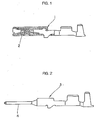
- a sample material of sample material number 6 in Table 4 which has been treated according to the present invention was press-formed to produce terminals shown in FIGS. 1 and 2, and then evaluated the material as the terminal.
- FIG. 1 shows a female terminal 1 having a spring portion 2 therein and FIG. 2 shows a male terminal 3 having a tab portion 4 therein. Insertion force the improvement of which is one of the objects of the alloy according to the present invention, as well as electrical characteristics were evaluated on them.
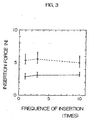
- the insertion force was measured with a load cell by inserting the male terminal shown in FIG. 2 into the female terminal shown in FIG. 1 made of the sample material at a speed of 10 mm/minute. Results of the measurements are shown in Table 5. Also, changes of the insertion force in accordance with the frequence of insertion are shown in FIG. 3, along with respective scattering ranges.
- a comparative sample material which is of the same base metal as the sample material of sample material number 6 and which has been subjected to the same plating treatment as the previous processing but has not been subjected to thermal diffusion treatment, is additionally shown in Table 4 as sample material number 12.
- the terminal which is capable of substantially decreasing the insertion force without increasing resistance and which has an excellent characteristic in wear resistance can be obtained with the alloy according to the present invention.
- a sample material having the same composition as that of the sample material of sample material number 6 was subjected to the same Sn coating treatment as the sample material of sample material number 6 and then the thus Sn-coated sample material was heated in a stream of hydrogen to prepare a comparative sample material having a Cu-Sn diffusion layer and an extremely thin oxide film formed on the surface. Insertion force of the resultant comparative sample material was measured in the same way as in the case of Example 2 and the result is additionally shown in Table 7. It is found from Table 7 that slipping property is enhanced and insertion force of the terminal is decreased by obtaining the oxide film thickness specified in the present invention.
- the copper or copper base alloy which has a thickness-controlled oxide film on an outermost surface thereof and a Cu-Sn system intermetallic compound under the oxide film
- the copper or copper base alloy provided with a wear resistant coating having a surface with large surface hardness, an excellent slipping property and a small friction coefficient
- this copper or copper base alloy has an excellent adhesion to the coating so that it has an excellent bending workability.
- it has an excellent electrical characteristic such as a small contact resistance, as well as a terminal made thereof has a small insertion force.
- the copper or copper base alloy is capable of being advantageously used in a connector material which is adaptable to the recent highly integrated electric equipment for use in an automobile or the like and an electrical part in which the wear resistance and corrosion resistance are required.
- wear resistant copper or copper base alloy having the above-described various characteristics can effectively and easily be produced.
- the copper or copper base alloy having an excellent surface characteristic such as surface roughness or the like after undergoing the heat treatment can effectively be obtained.
Landscapes
- Chemical & Material Sciences (AREA)
- Organic Chemistry (AREA)
- Engineering & Computer Science (AREA)
- Materials Engineering (AREA)
- Metallurgy (AREA)
- Mechanical Engineering (AREA)
- Crystallography & Structural Chemistry (AREA)
- Physics & Mathematics (AREA)
- Thermal Sciences (AREA)
- Chemical Kinetics & Catalysis (AREA)
- Electrochemistry (AREA)
- Electroplating Methods And Accessories (AREA)
- Other Surface Treatments For Metallic Materials (AREA)
- Conductive Materials (AREA)
Abstract
Description
| Sample Material Numbers | Sn Film Thickness (µm) | Presence (Yes) or Absence (No) of Reflow Treatment | Oxide Film Thickness (nm) | Base Metals (wt%) | |
| Examples | 1 | 1.0 | No | 290 | Oxygen-free Copper |
| 2 | 0.6 | No | 30 | Cu-30Zn | |
| 3 | 1.1 | Yes | 30 | Cu-30Zn | |
| 4 | 0.8 | Yes | 30 | Cu-2Sn-0.1Fe-0.03P | |
| 5 | 1.9 | No | 20 | Cu-1Ni-0.9Sn-0.05P | |
| 6 | 1.1 | Yes | 25 | Cu-1Ni-0.9Sn-0.05P | |
| 7 | 2.5 | Yes | 140 | Cu-2Sn-0.1Fe-0.03P | |
| Comparative Examples | 8 | 12 | No | 500 | Oxygen-free Copper |
| 9 | 2.0 | No | 1400 | Cu-30Zn | |
| 10 | 0.08 | No | 120 | Cu-1Ni-0.9Sn-0.05P |
| Sample Material Numbers | Surface Vickers Hardness (Hv) | Contact Resistance (mΩ) | Bending Workability | Adhesivity | |
| Examples | 1 | 270 | 7 | ○ | ○ |
| 2 | 300 | 10 | ○ | ○ | |
| 3 | 310 | 8 | ○ | ○ | |
| 4 | 290 | 9 | ○ | ○ | |
| 5 | 340 | 9 | ○ | ○ | |
| 6 | 350 | 8 | ○ | ○ | |
| 7 | 390 | 10 | ○ | ○ | |
| Comparative Examples | 8 | 310 | 5 | X | ○ |
| 9 | 325 | 130 | ○ | X | |
| 10 | 210 | 32 | ○ | ○ |
| Sample Material Numbers | Presence (Yes) or Absence (No) of Reflow Treatment | Surface Roughness before Heat Treatment (µm) | Surface Roughness after Heat Treatment (µm) | ||
| Ra | Rmax | Ra | Rmax | ||
| 6 | Yes | 0.05 | 0.67 | 0.07 | 0.92 |
| 11 | No | 0.07 | 0.85 | 0.13 | 1.89 |
| Sample Material Numbers | Presence of Heat Treatment | Sn Film Thickness (µm) | Oxide Film Thickness (nm) | Base Materials (wt%) | |
| Examples | 6 | Yes | 1.1 | 25 | Cu-1Ni-0.9Sn-0.05P |
| Comparative Examples | 12 | No | 1.1 | 6 | Cu-1Ni-0.9Sn-0.05P |
| Sample Material Numbers | Vickers Hardness (Hv) | Frequence Of Insertion | Insertion Force (N) |
| Examples 6 | 350 | First time | 2.85 |
| Third time | 3.11 | ||
| Tenth time | 3.28 | ||
| Comparative Examples 12 | 116 | First time | 5.35 |
| Third time | 5.57 | ||
| Tenth time | 5.01 |
| Sample Material Numbers | Initial Contact Resistance (mΩ) | Contact Resistance (mΩ) after 10 Times of Insertion/Extraction Operations |
| Examples 6 | 1.8 | 1.9 |
| Comparative Examples 12 | 1.7 | 1.9 |
| Sample Material Numbers | Oxide Film (nm) | Insertion Force (N) |
| Examples 6 | 25 | 2.85 |
| Comparative Examples 12 | 7 | 3.38 |
Claims (9)
- Wear resistant copper or a wear resistant copper base alloy having formed on the outermost surface thereof an oxide film layer having a thickness of 10-1000 nm and a layer of an intermetallic compound primarily comprising Cu-Sn under the oxide film layer.
- Wear resistant copper or a wear resistant copper base alloy having formed on the outermost surface thereof an oxide film layer having a thickness of 10-1000 nm and a layer of an intermetallic compound primarily comprising Cu-Sn having a thickness of 0.1-10 µm under the oxide film layer.
- The wear resistant copper or copper base alloy according to Claim 1 or 2, wherein contact resistance thereof is 60mΩ or less.
- The copper or copper base alloy according to Claim 1, 2 or 3, wherein surface hardness thereof is Hv 250 or more.
- A method of preparing wear resistant copper or a wear resistant copper base alloy comprising the steps of:coating copper or a copper base alloy with Sn; andperforming heat treatment to thereby form an oxide film layer having a thickness of 10-1000 nm on the outermost surface thereof and a layer of an intermetallic compound primarily comprising Cu-Sn under the oxide film layer.
- The method according to claim 5, wherein the layer of an intermetallic compound which primarily comprises Cu-Sn is formed to have a thickness of 0.1 to 10 µm.
- The method according to claim 5 or claim 6, which comprises between the step of coating copper or a copper base alloy with Sn and the step of performing heat-treatment the additional step of performing reflow treatment.
- An electrical part comprising wear resistant copper or a wear resistant copper base alloy, wherein the wear resistant copper or the wear resistant copper base alloy is as defined in any of the claims 1 to 4.
- An electrical part comprising wear-resistant or a wear-resistant copper base alloy wherein the wear-resistant copper or the wear-resistant copper base alloy has been prepared by the method according to any of the claims 5 to 7.
Applications Claiming Priority (2)
| Application Number | Priority Date | Filing Date | Title |
|---|---|---|---|
| JP1787599 | 1999-01-27 | ||
| JP01787599A JP3465876B2 (en) | 1999-01-27 | 1999-01-27 | Wear-resistant copper or copper-based alloy, method for producing the same, and electric component comprising the wear-resistant copper or copper-based alloy |
Publications (2)
| Publication Number | Publication Date |
|---|---|
| EP1024212A2 true EP1024212A2 (en) | 2000-08-02 |
| EP1024212A3 EP1024212A3 (en) | 2001-09-05 |
Family
ID=11955871
Family Applications (1)
| Application Number | Title | Priority Date | Filing Date |
|---|---|---|---|
| EP00101518A Ceased EP1024212A3 (en) | 1999-01-27 | 2000-01-26 | Wear resistant copper or copper base alloy, method of preparing the same and electrical part using the same |
Country Status (3)
| Country | Link |
|---|---|
| US (1) | US6336979B1 (en) |
| EP (1) | EP1024212A3 (en) |
| JP (1) | JP3465876B2 (en) |
Cited By (6)
| Publication number | Priority date | Publication date | Assignee | Title |
|---|---|---|---|---|
| EP1182737A1 (en) * | 2000-08-24 | 2002-02-27 | Sumitomo Wiring Systems, Ltd. | Electrical connector housing |
| EP1288321A1 (en) * | 2001-08-21 | 2003-03-05 | STOLBERGER METALLWERKE GMBH & CO. KG | Material for a metal strip |
| FR2832257A1 (en) * | 2001-11-13 | 2003-05-16 | Yazaki Corp | THICK HEADED |
| EP1788585A4 (en) * | 2004-09-10 | 2008-07-09 | Kobe Steel Ltd | CONDUCTIVE MATERIAL FOR CONNECTING PART AND METHOD FOR MANUFACTURING CONDUCTIVE MATERIAL |
| EP3439114A4 (en) * | 2016-03-31 | 2019-08-28 | Nisshin Steel Co., Ltd. | Automotive terminal |
| EP3438331A4 (en) * | 2016-03-31 | 2019-08-28 | Nisshin Steel Co., Ltd. | CONNECTING COMPONENT MATERIAL |
Families Citing this family (21)
| Publication number | Priority date | Publication date | Assignee | Title |
|---|---|---|---|---|
| DE10025106A1 (en) * | 2000-05-20 | 2001-11-22 | Stolberger Metallwerke Gmbh | Electrically conductive metal tape and connectors from it |
| DE10025107A1 (en) * | 2000-05-20 | 2001-11-22 | Stolberger Metallwerke Gmbh | Electrically conductive metal band and connector |
| TW575688B (en) * | 2001-01-19 | 2004-02-11 | Furukawa Electric Co Ltd | Metal-plated material and method for preparation thereof, and electric and electronic parts using the same |
| US20050037229A1 (en) * | 2001-01-19 | 2005-02-17 | Hitoshi Tanaka | Plated material, method of producing same, and electrical / electronic part using same |
| JP2002226982A (en) * | 2001-01-31 | 2002-08-14 | Dowa Mining Co Ltd | Heat resistant coating, method for producing the same, and electric / electronic component |
| KR100513947B1 (en) * | 2002-03-29 | 2005-09-09 | 닛코 킨조쿠 가부시키가이샤 | A copper alloy having good pressing workability and manufacturing method therefor |
| CN100460570C (en) * | 2002-06-13 | 2009-02-11 | 日本新铬电镀株式会社 | Copper-tin-oxygen alloy coating |
| US7867625B2 (en) * | 2002-06-13 | 2011-01-11 | Nihon New Chrome Co., Ltd. | Copper-tin-oxygen alloy plating |
| JP4525285B2 (en) * | 2004-10-12 | 2010-08-18 | 富士通株式会社 | Electronic component and manufacturing method thereof |
| JP4814552B2 (en) * | 2005-06-13 | 2011-11-16 | Dowaメタルテック株式会社 | Surface treatment method |
| JP4934456B2 (en) | 2006-02-20 | 2012-05-16 | 古河電気工業株式会社 | Plating material and electric / electronic component using the plating material |
| JP4868892B2 (en) * | 2006-03-02 | 2012-02-01 | 富士通株式会社 | Plating method |
| CN101682135B (en) | 2007-04-09 | 2013-10-02 | 古河电气工业株式会社 | Connector and metallic material for connector |
| CN101688312B (en) | 2007-06-29 | 2012-02-29 | 古河电气工业株式会社 | Metal material, manufacturing method thereof, and electrical and electronic parts using the same |
| JP4964795B2 (en) * | 2008-01-23 | 2012-07-04 | Jx日鉱日石金属株式会社 | Copper alloy tin plating strip with excellent wear resistance |
| JP5185759B2 (en) * | 2008-10-03 | 2013-04-17 | Dowaメタルテック株式会社 | Conductive material and manufacturing method thereof |
| JP5490144B2 (en) * | 2009-12-25 | 2014-05-14 | Ykk株式会社 | Fastener components and slide fasteners |
| US9224550B2 (en) | 2012-12-26 | 2015-12-29 | Tyco Electronics Corporation | Corrosion resistant barrier formed by vapor phase tin reflow |
| JP5895973B2 (en) * | 2014-06-12 | 2016-03-30 | 第一精工株式会社 | Conductive terminal |
| JP5907300B1 (en) * | 2015-04-30 | 2016-04-26 | 第一精工株式会社 | Conductive terminal |
| CN109155479A (en) | 2016-05-12 | 2019-01-04 | 住友电装株式会社 | terminal part |
Family Cites Families (9)
| Publication number | Priority date | Publication date | Assignee | Title |
|---|---|---|---|---|
| JPH01225781A (en) * | 1988-03-05 | 1989-09-08 | Kobe Steel Ltd | Tin or tin alloy-coated copper alloy material having excellent whisker resistance |
| JPH02173294A (en) * | 1988-12-26 | 1990-07-04 | Nippon Mining Co Ltd | Reflow treatment of tin or tin alloy plated material |
| JP3903326B2 (en) * | 1993-11-05 | 2007-04-11 | Dowaホールディングス株式会社 | Copper-based alloy and its manufacturing method |
| US5849424A (en) * | 1996-05-15 | 1998-12-15 | Dowa Mining Co., Ltd. | Hard coated copper alloys, process for production thereof and connector terminals made therefrom |
| JP3408929B2 (en) * | 1996-07-11 | 2003-05-19 | 同和鉱業株式会社 | Copper-based alloy and method for producing the same |
| JP3722172B2 (en) * | 1996-08-24 | 2005-11-30 | 株式会社神戸製鋼所 | Tin or tin alloy plated copper alloy for multipolar terminals and method for producing the same |
| EP0834602A1 (en) * | 1996-09-26 | 1998-04-08 | The Whitaker Corporation | Process for protecting a silver surface and electrical contact with a silver surface |
| JP2000164279A (en) * | 1998-11-30 | 2000-06-16 | Kobe Steel Ltd | Sn-plated copper alloy material for terminals and connectors |
| JP2001169995A (en) | 1999-12-20 | 2001-06-26 | Azuma Kogyo Kk | Cleaning implement |
-
1999
- 1999-01-27 JP JP01787599A patent/JP3465876B2/en not_active Expired - Lifetime
-
2000
- 2000-01-26 EP EP00101518A patent/EP1024212A3/en not_active Ceased
- 2000-01-27 US US09/493,997 patent/US6336979B1/en not_active Expired - Lifetime
Cited By (9)
| Publication number | Priority date | Publication date | Assignee | Title |
|---|---|---|---|---|
| EP1182737A1 (en) * | 2000-08-24 | 2002-02-27 | Sumitomo Wiring Systems, Ltd. | Electrical connector housing |
| US6814591B2 (en) | 2000-08-24 | 2004-11-09 | Sumitomo Wiring Systems, Ltd. | Electrical connector housing |
| EP1288321A1 (en) * | 2001-08-21 | 2003-03-05 | STOLBERGER METALLWERKE GMBH & CO. KG | Material for a metal strip |
| FR2832257A1 (en) * | 2001-11-13 | 2003-05-16 | Yazaki Corp | THICK HEADED |
| EP1788585A4 (en) * | 2004-09-10 | 2008-07-09 | Kobe Steel Ltd | CONDUCTIVE MATERIAL FOR CONNECTING PART AND METHOD FOR MANUFACTURING CONDUCTIVE MATERIAL |
| US7820303B2 (en) | 2004-09-10 | 2010-10-26 | Kabushiki Kaisha Kobe Seiko Sho (Kobe Steel, Ltd.) | Conductive material for connecting part and method for manufacturing the conductive material |
| US8445057B2 (en) | 2004-09-10 | 2013-05-21 | Kobe Steel, Ltd. | Conductive material for connecting part and method for manufacturing the conductive material |
| EP3439114A4 (en) * | 2016-03-31 | 2019-08-28 | Nisshin Steel Co., Ltd. | Automotive terminal |
| EP3438331A4 (en) * | 2016-03-31 | 2019-08-28 | Nisshin Steel Co., Ltd. | CONNECTING COMPONENT MATERIAL |
Also Published As
| Publication number | Publication date |
|---|---|
| US6336979B1 (en) | 2002-01-08 |
| JP3465876B2 (en) | 2003-11-10 |
| JP2000212720A (en) | 2000-08-02 |
| EP1024212A3 (en) | 2001-09-05 |
Similar Documents
| Publication | Publication Date | Title |
|---|---|---|
| US6336979B1 (en) | Wear resistant copper base alloy, method of preparing the same and electrical part using the same | |
| JP3408929B2 (en) | Copper-based alloy and method for producing the same | |
| CA2240239C (en) | Tin coated electrical connector | |
| US5849424A (en) | Hard coated copper alloys, process for production thereof and connector terminals made therefrom | |
| CN100528550C (en) | Heat-resistant protective film, method for producing same, and electrical and electronic component | |
| KR101682791B1 (en) | A copper alloy sheet with sn coating layer for a fitting type connection terminal and a fitting type connection terminal | |
| EP1026287B1 (en) | Process for production of copper or copper base alloys | |
| EP2743381B1 (en) | Tin-plated copper alloy terminal member with outstanding insertion and removal characteristics | |
| EP2267187A1 (en) | Connecting component metal material and manufacturing method thereof | |
| JP4538813B2 (en) | Connector and charging socket using copper-based alloy material | |
| JP2003293187A (en) | Plated copper or copper alloy and method for producing the same | |
| TWI752184B (en) | Corrosion-resistant terminal material, corrosion-resistant terminal, and wire termination structure | |
| CN108790320A (en) | Electronic component-use metal material and its manufacturing method, bonder terminal, connector and electronic unit using it | |
| JP2008223143A (en) | Plating material, manufacturing method thereof, and electric / electronic parts using the same | |
| JP4814552B2 (en) | Surface treatment method | |
| JP7773020B2 (en) | Connector terminal material | |
| JP3903326B2 (en) | Copper-based alloy and its manufacturing method | |
| JP5436391B2 (en) | Film and electrical / electronic parts | |
| JP4427487B2 (en) | Tin-coated electrical connector | |
| JP5155139B2 (en) | Tin-coated electrical connector | |
| JPH03219064A (en) | Electronic equipment parts |
Legal Events
| Date | Code | Title | Description |
|---|---|---|---|
| PUAI | Public reference made under article 153(3) epc to a published international application that has entered the european phase |
Free format text: ORIGINAL CODE: 0009012 |
|
| AK | Designated contracting states |
Kind code of ref document: A2 Designated state(s): DE GB |
|
| AX | Request for extension of the european patent |
Free format text: AL;LT;LV;MK;RO;SI |
|
| PUAL | Search report despatched |
Free format text: ORIGINAL CODE: 0009013 |
|
| AK | Designated contracting states |
Kind code of ref document: A3 Designated state(s): DE GB |
|
| AX | Request for extension of the european patent |
Free format text: AL;LT;LV;MK;RO;SI |
|
| 17P | Request for examination filed |
Effective date: 20020222 |
|
| AKX | Designation fees paid |
Free format text: DE GB |
|
| RAP1 | Party data changed (applicant data changed or rights of an application transferred) |
Owner name: DOWA MINING CO., LTD. Owner name: YAZAKI CORPORATION |
|
| 17Q | First examination report despatched |
Effective date: 20070702 |
|
| RAP1 | Party data changed (applicant data changed or rights of an application transferred) |
Owner name: DOWA HOLDINGS CO., LTD. Owner name: YAZAKI CORPORATION |
|
| RAP1 | Party data changed (applicant data changed or rights of an application transferred) |
Owner name: YAZAKI CORPORATION Owner name: DOWA METALTECH CO., LTD. |
|
| RAP1 | Party data changed (applicant data changed or rights of an application transferred) |
Owner name: DOWA METALTECH CO., LTD. |
|
| STAA | Information on the status of an ep patent application or granted ep patent |
Free format text: STATUS: THE APPLICATION HAS BEEN REFUSED |
|
| 18R | Application refused |
Effective date: 20120730 |