EP1023962B1 - Cutting tool with means to control the chip flow - Google Patents
Cutting tool with means to control the chip flow Download PDFInfo
- Publication number
- EP1023962B1 EP1023962B1 EP00101195A EP00101195A EP1023962B1 EP 1023962 B1 EP1023962 B1 EP 1023962B1 EP 00101195 A EP00101195 A EP 00101195A EP 00101195 A EP00101195 A EP 00101195A EP 1023962 B1 EP1023962 B1 EP 1023962B1
- Authority
- EP
- European Patent Office
- Prior art keywords
- cutting tool
- cutting
- chip
- tool
- layer
- Prior art date
- Legal status (The legal status is an assumption and is not a legal conclusion. Google has not performed a legal analysis and makes no representation as to the accuracy of the status listed.)
- Expired - Lifetime
Links
Images

Classifications
-
- B—PERFORMING OPERATIONS; TRANSPORTING
- B23—MACHINE TOOLS; METAL-WORKING NOT OTHERWISE PROVIDED FOR
- B23B—TURNING; BORING
- B23B27/00—Tools for turning or boring machines; Tools of a similar kind in general; Accessories therefor
- B23B27/14—Cutting tools of which the bits or tips or cutting inserts are of special material
- B23B27/141—Specially shaped plate-like cutting inserts, i.e. length greater or equal to width, width greater than or equal to thickness
-
- B—PERFORMING OPERATIONS; TRANSPORTING
- B23—MACHINE TOOLS; METAL-WORKING NOT OTHERWISE PROVIDED FOR
- B23B—TURNING; BORING
- B23B2226/00—Materials of tools or workpieces not comprising a metal
- B23B2226/31—Diamond
-
- B—PERFORMING OPERATIONS; TRANSPORTING
- B23—MACHINE TOOLS; METAL-WORKING NOT OTHERWISE PROVIDED FOR
- B23B—TURNING; BORING
- B23B2226/00—Materials of tools or workpieces not comprising a metal
- B23B2226/31—Diamond
- B23B2226/315—Diamond polycrystalline [PCD]
-
- Y—GENERAL TAGGING OF NEW TECHNOLOGICAL DEVELOPMENTS; GENERAL TAGGING OF CROSS-SECTIONAL TECHNOLOGIES SPANNING OVER SEVERAL SECTIONS OF THE IPC; TECHNICAL SUBJECTS COVERED BY FORMER USPC CROSS-REFERENCE ART COLLECTIONS [XRACs] AND DIGESTS
- Y10—TECHNICAL SUBJECTS COVERED BY FORMER USPC
- Y10T—TECHNICAL SUBJECTS COVERED BY FORMER US CLASSIFICATION
- Y10T407/00—Cutters, for shaping
- Y10T407/26—Cutters, for shaping comprising cutting edge bonded to tool shank
-
- Y—GENERAL TAGGING OF NEW TECHNOLOGICAL DEVELOPMENTS; GENERAL TAGGING OF CROSS-SECTIONAL TECHNOLOGIES SPANNING OVER SEVERAL SECTIONS OF THE IPC; TECHNICAL SUBJECTS COVERED BY FORMER USPC CROSS-REFERENCE ART COLLECTIONS [XRACs] AND DIGESTS
- Y10—TECHNICAL SUBJECTS COVERED BY FORMER USPC
- Y10T—TECHNICAL SUBJECTS COVERED BY FORMER US CLASSIFICATION
- Y10T407/00—Cutters, for shaping
- Y10T407/27—Cutters, for shaping comprising tool of specific chemical composition
Definitions
- this is conveniently 0.5 to 3.0 mm over the layer of PCD and PKB over and is on its side facing the cutting edge beveled by approximately 40 to 50 °.
- the one facing the cutting edge Top edge of the chip breaker with a radius for example be rounded by 0.5 mm.
- the step-shaped recess 60 makes it possible to place one over the carrier body 62 of the cutting tool 54 on the side facing away from the cutting edges 56
- the both with the holder 52 and with the carrier body 62 is soldered.
- the chip breaker 64 is welded on , it is recommended to place it at the rear end where it is with the holder 52 is to be welded on the underside with a flat projection, like with a boot heel.
- This advantage of e.g. B. about 1 to 2 tenths Millimeter height ensures with a flat contact surface reliable and uniform on the carrier and holder Pressure against the holder during the welding process.
- Chip breaker is also the application of chip breakers conceivable on the carrier bodies of the cutting tool inserts, whose job is not to break up the chips short length, but arising in a targeted derivation Chips exist.
Description
Die Erfindung befaßt sich mit einem Schneidwerkzeug mit im Bereich der Spanfläche angeordneten Mitteln zur Verhinderung unkontrollierter Spanbildung, die in einem bestimmten Abstand zu einer Schneidkante an einer Schicht aus polykristallinem Diamant (PKD) oder polykristallinem Bornitrid (PKB) angeordnet sind, die auf einem Trägerkörper aufgebracht ist.The invention relates to a cutting tool with Prevention means arranged in the area of the rake face uncontrolled chip formation that occurs in a particular Distance to a cutting edge on a layer of polycrystalline Diamond (PCD) or polycrystalline boron nitride (PKB) are arranged, which are applied to a carrier body is.
Bei der spanabhebenden Bearbeitung von insbesondere zähen Werkstoffen, wie z. B. Nichteisenmetallen oder Kunststoffen, ist man bestrebt, die unkontrollierte Bildung langer Späne zu unterbinden, da diese u. a. die bearbeiteten Oberflächen beschädigen können. Hierzu sind sog. Spanbrecher, welche die Späne auf kurze Länge brechen, und Spanleitstufen bekannt, welche die langen Späne gezielt von dem Arbeitsbereich wegleiten. Da derartige Mittel zur Verhinderung unkontrollierter Spanbildung möglichst nahe an der Schneidkante angeordnet sein sollten, um effektiv arbeiten zu können, ergibt sich bei Schneidwerkzeugen mit Schneidwerkstoffen aus polykristallinem Diamant (PKD) oder polykristallinem Bornitrid (PKB) das Problem, daß die aus diesen Werkstoffen bestehende Schicht die Spanfläche bildet und auf dieser Schicht keine separaten Mittel zuverlässig befestigt werden können. Man behilft sich daher damit, die Schneidwerkzeuge in einem Schlitz eines Werkzeughalters einzulöten, wobei jedoch lediglich eine Lötverbindung zwischen dem Trägerkörper und dem Schlitz möglich ist und zwischen der Oberfläche der Schicht aus PKD bzw. PKB und den Mitteln zur Spankontrolle eine schmale Fuge verbleibt. Es hat sich gezeigt, daß sich Späne in dieser Fuge festsetzen können, wodurch einerseits der Werkzeugträger schnell verschleißt und andererseits Beschädigungen der Werkstoffoberfläche auftreten können. Schneidwerkzeuge mit Mitteln zur Spankontrolle sind aus der US 4,854,784 und der US 5,405,711 bekannt.When machining especially tough Materials such as B. non-ferrous metals or plastics, one strives to keep the uncontrolled formation longer To prevent chips, as this a. the machined surfaces can damage. This includes so-called chip breakers, which break the chips to a short length, and chip breakers known which targeted the long chips from the work area divert. Because such means of prevention uncontrolled chip formation as close as possible to the Cutting edge should be arranged to work effectively the ability to use cutting tools with cutting materials made of polycrystalline diamond (PCD) or polycrystalline Boron nitride (PKB) the problem that comes from this The existing layer forms the rake face and no separate means reliable on this layer can be attached. One therefore helps oneself with the Cutting tools in a slot in a tool holder solder, but only a solder connection between the support body and the slot is possible and between the surface of the layer of PCD or PKB and the A narrow joint remains for means of chip control. It has been shown that chips settle in this joint can, which means that the tool holder wears out quickly and on the other hand damage to the material surface may occur. Cutting tools with means for Chip control are known from US 4,854,784 and US 5,405,711.
Die Aufgabe der Erfindung besteht darin, ein Schneidwerkzeug mit einem Schneidwerkstoff aus PKD bzw. PKB zu schaffen, das Mittel zur Spankontrolle ohne Fuge zur Spanfläche in der Nähe der Schneidkante ermöglicht.The object of the invention is a cutting tool to create with a cutting material made of PCD or PCB, the means for chip control without a joint to the chip surface near the cutting edge.
Erfindungsgemäß wird die Aufgabe dadurch gelöst, daß die Schicht aus PKD bzw. PKB im Bereich der Mittel zur Verhinderung unkontrollierter Spanbildung bis auf den Trägerkörper ausgespart und die Mittel zur Verhinderung unkontrollierter Spanbildung dort unmittelbar auf dem Trägerkörper aufgebracht sind.According to the invention the object is achieved in that the Layer of PKD or PKB in the area of the means for prevention uncontrolled chip formation down to the carrier body recessed and the means to prevent uncontrolled Chip formation there directly on the carrier body are upset.
Das nachträgliche Abtragen der Schicht aus PKD bzw. PKB im Bereich der Aussparung beispielsweise im Wege der Elektroerosion erlaubt eine präzise Annäherung an die Schneidkante auf einen Abstand, der bei der Herstellung der Schicht nicht erreichbar wäre. Die präzise Einhaltung des Abstandes der Mittel zur Verhinderung unkontrollierter Spanbildung von vorzugsweise ungefähr 0,3 bis 1,5 mm führt nicht zu einer Erhöhung der Gefahr von Sprödbrüchen der sehr empfindlichen Schneidwerkstoffe.The subsequent removal of the layer of PKD or PKB in the Area of the recess, for example by means of electrical discharge machining allows a precise approach to the cutting edge at a distance during the production of the layer would not be reachable. The precise observance of the distance the means to prevent uncontrolled chip formation of preferably about 0.3 to 1.5 mm does not result in one Increasing the risk of brittle fractures of the very sensitive Cutting materials.
Ein weiterer Vorteil der Erfindung besteht darin, daß sich das erfindungsgemäße Schneidwerkzeug auf sehr wirtschaftliche Weise herstellen läßt und auf dem Trägerkörper von der Form her praktisch beliebige Mittel zur Spankontrolle aufgebracht werden können. Da diese in der Nähe der Schneidkante an dem Trägerkörper verankert sind, ergibt sich auch ein sehr fester Halt dieser Mittel, da im Vergleich zu den bisher üblichen Lösungen nur ein sehr geringer Hebelweg zwischen dem Angriffspunkt der Späne und dem Verankerungspunkt der Mittel zur Spankontrollierung an dem Trägerkörper vorliegt. Die Nähe des Verankerungspunktes an der Schneidkante erlaubt daher auch die Ausbildung relativ hoher Spanbrech- oder Spanleitmittel, falls dies gewünscht sein sollte.Another advantage of the invention is that the cutting tool according to the invention on very economical Can be made and on the carrier body of the Form practically any means for chip control applied can be. Because this is near the cutting edge are also anchored to the carrier body a very firm hold of these funds as compared to the previously common solutions only a very small leverage between the point of attack of the chips and the anchor point the means for chip control on the carrier body is present. The proximity of the anchor point to the cutting edge therefore also allows the formation of relatively high chip breaking or chip guide, if this should be desired.
Die Stärke der Schicht aus PKD bzw. PKB beträgt vorzugsweise ungefähr 0,3 bis 1,5 mm. Derartige Schichtdicken lassen sich mit den bekannten Herstellungsverfahren für Schneidwerkzeuge erzielen, wobei dünne Schichtdicken den Vorteil bieten, daß der Elektroerosionsvorgang weniger zeitaufwendig ist und damit geringere Kosten verursacht. Besonders günstig für die Ausbildung der Aussparung ist es dabei, wenn die Schicht aus PKD bzw. PKB durch Abscheiden des Schneidwerkstoffes in der Dampfphase auf den Trägerkörper aufgebracht ist, da die auf diese Weise herstellbaren Überzüge, beispielsweise aus Diamant, nur eine geringe Schichtdicke besitzen und daher bei der Bearbeitung elektroerosiv besonders leicht zu durchdringen sind.The thickness of the layer of PCD or PKB is preferably about 0.3 to 1.5 mm. Let such layer thicknesses with the known manufacturing processes for Cutting tools achieve, with thin layer thicknesses Offer advantage that the electroerosion process less is time-consuming and therefore causes lower costs. It is particularly favorable for the formation of the recess when the layer of PKD or PKB is deposited of the cutting material in the vapor phase on the carrier body is applied because the producible in this way Coatings, for example made of diamond, are only slight Have layer thickness and therefore electroerosive during processing are particularly easy to penetrate.
Das erfindungsgemäß Schneidwerkzeug kann als Einsatz für einen Halter oder als Wendeschneidplatte mit mehreren Schneidkanten ausgebildet sein.The cutting tool according to the invention can be used for a holder or as an indexable insert with several Cutting edges should be formed.
Die Mittel zur Verhinderung unkontrollierter Spanbildung können allseitig von einem verbleibenden Steg der Schicht aus PKD bzw. PKB umgeben sein. In diesem Fall sind die Kontrollmittel ausschließlich am Trägerkörper des Schneidwerkzeuges befestigt. Je nach Einsatzart kann es auch zweckmässig sein, die Schicht aus PKD bzw. PKB zu einem Rand eines Halters hin vollständig zu entfernen, so daß die Kontrollmittel sowohl mit dem Trägerkörper des Schneidwerkzeuges als auch mit dessen Halter verlötet, verschweißt oder verklebt werden können, um eine zusätzliche Stabilität zu erzeugen.The means to prevent uncontrolled chip formation can on all sides of a remaining web of the layer be surrounded by PKD or PKB. In this case, the means of control only on the carrier body of the cutting tool attached. Depending on the type of use, it can also be useful be the layer of PKD or PKB to an edge of a To remove the holder completely so that the control means both with the carrier body of the cutting tool as well as soldered, welded or glued to its holder can be added stability produce.
Vorzugsweise bestehen die Mittel zur Verhinderung unkontrollierter Spanbildung und/oder der Trägerkörper aus Hartmetall oder hochlegiertem Cr-W-Werkzeugstahl (Schnellarbeitsstahl). Besonders ideal ist es, beide Teile aus Hartmetall herzustellen, da dieses gegen Beschädigungen durch die Späne besonders resistent ist und eine gute Verbindung zwischen den Kontrollmitteln und dem Trägerkörper beispielsweise durch Verlöten ermöglichen. Andererseits lassen sich Teile aus Stahl besser verschweißen.Preferably, the means to prevent uncontrolled existence Chip formation and / or the carrier body made of hard metal or high-alloy Cr-W tool steel (high-speed steel). It is particularly ideal to have both parts made of hard metal to manufacture, as this against damage by the chips are particularly resistant and a good connection between the control means and the carrier body, for example enable by soldering. On the other hand, leave parts made of steel weld better.
Je nach Einsatzgebiet des Schneidwerkzeuges und des zu zerspanenden Werkstoffes können die Mittel zur Verhinderung unkontrollierter Spanbildung als Spanleitstufe zum Wegführen sich bildender Späne oder als Spanbrecher zum Verkürzen der Späne auf eine unschädliche Länge ausgebildet sein.Depending on the area of application of the cutting tool and the one to be cut Material can be the means of prevention uncontrolled chip formation as chip breaker to lead away forming chips or as a chip breaker for shortening the chips must be of an innocuous length.
Bei der Ausbildung als Spanbrecher steht dieser zweckmäßigerweise 0,5 bis 3,0 mm über die Schicht aus PKD und PKB über und ist an seiner der Schneidkante zugewandten Flanke um ungefähr 40 bis 50° abgeschrägt. Alternativ oder ergänzend zu der Abschrägung kann die der Schneidkante zugewandte Oberkante des Spanbrechers mit einem Radius, beispielsweise von 0,5 mm abgerundet sein.When training as a chipbreaker, this is conveniently 0.5 to 3.0 mm over the layer of PCD and PKB over and is on its side facing the cutting edge beveled by approximately 40 to 50 °. Alternatively or in addition to the bevel, the one facing the cutting edge Top edge of the chip breaker with a radius, for example be rounded by 0.5 mm.
Es versteht sich, daß das erfindungsgemäße Schneidwerkzeug in allen seinen möglichen Ausführungsformen als Bohr-, Fräs- oder Drehwerkzeug ausgebildet sein kann. It is understood that the cutting tool according to the invention in all its possible embodiments as drilling, Milling or turning tool can be formed.
Nachfolgend wird anhand der beigefügten Zeichnungen näher auf Ausführungsbeispiele der Erfindung eingegangen. Es zeigen:
- Fig. 1
- eine Draufsicht eines Werkzeuges;
- Fig. 2
- einen Längsschnitt des Werkzeuges nach Fig. 1;
- Fig. 3
- eine Draufsicht auf ein weiteres Werkzeug mit unterschiedlich ausgebildetem Spanbrecher;
- Fig. 4
- einen Längsschnitt des Werkzeuges nach Fig. 3;
- Fig. 5
- eine Draufsicht auf eine weitere Ausführungsform eines Werkzeuges mit Spanbrecher;
- Fig. 6
- einen Längsschnitt des Werkzeuges nach Fig. 5.
- Fig. 1
- a plan view of a tool;
- Fig. 2
- a longitudinal section of the tool of FIG. 1;
- Fig. 3
- a plan view of another tool with differently designed chip breaker;
- Fig. 4
- a longitudinal section of the tool of FIG. 3;
- Fig. 5
- a plan view of a further embodiment of a tool with chip breaker;
- Fig. 6
- 5 shows a longitudinal section of the tool according to FIG. 5.
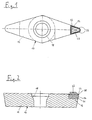
In Fig. 1 ist ein Werkzeug 10 dargestellt, das im wesentlichen
aus einem Halter 12 und einem Schneidwerkzeugeinsatz
14 besteht. Der Schneidwerkzeugeinsatz 14 sitzt in einer
entsprechend geformten Aussparung 16 an einem Ende des Halters
12, der mittig mit einer Befestigungsbohrung 18 versehen
ist, die eine präzise Befestigung des Werkzeuges 10 an
einem weiteren Halter (nicht gezeigt) ermöglicht.In Fig. 1, a
Der Schneidwerkzeugeinsatz 14 besteht im wesentlichen aus
einem Trägerkörper 20, einem auf diesen aufgelöteten Spanbrecher
22 und einer auf dem Trägerkörper 20 aufgebrachten
Schicht 24 aus polykristallinem Diamant (PKD), die sich anschmiegend
um den Spanbrecher 22 erstreckt. Sowohl der Trägerkörper
20 als auch der Spanbrecher 22 bestehen aus Hartmetall.
Der Trägerkörper 20 ist mit der Aussparung 16 verlötet,
so daß der Schneidwerkzeugeinsatz 14 materialschlüssig
fest mit dem Halter 12 verbunden ist.The
Die Herstellung des Schneidwerkzeugeinsatzes 14 erfolgt in
der Weise, daß zunächst auf dem Trägerkörper 20 eine
Schicht aus PKD von einer Dicke im vorliegenden Fall von
0,3 mm aufgebracht wird. Neben den herkömmlichen Verfahren
ist es auch denkbar, den Diamantwerkstoff durch Abscheidung
aus der Dampfphase aufzubringen.The
Anschließend wird im Wege des Profilsenkerodierens oder
mittels Laser oder eines anderen geigneten Erodier- oder
Verdampfungsverfahrens die Schicht im mittleren Bereich bis
auf den Trägerkörper 16 entfernt, so daß zwischen dem Spanbrecher
22 und den Schneidkanten 26 des Schneidwerkzeugeinsatzes
14 nur ein Steg von ungefähr 0,3 bis 1,5 mm Breite
verbleibt. Auch in dem an der Aussparung 16 anliegenden Bereich
verbleibt bei dem Schneidwerkzeugeinsatz 14 ein Steg
von 0,4 mm Breite. Anschließend wird der Spanbrecher 22,
dessen den Schneidkanten zugewandte Flanken 28 um ungefähr
45° abgeschrägt sind, unmittelbar auf dem Trägerkörper 20
aufgelötet. Das Elektroerodieren erlaubt ein derart präzises
Aussparen der PKD-Schicht 24, daß es nicht zu einer wesentlichen
Schwächung des Schneidwerkstoffes kommt, so daß
keine Gefahr von Sprödbrüchen besteht.Then EDM or
by means of a laser or another suitable eroding or
Evaporation process up the layer in the middle
removed on the
Die Aussparung 16 ist im gezeigten Beispiel so tief ausgebildet,
daß die Oberkante der PKD-Schicht 24 bündig mit der
Oberfläche des Halters 12 abschließt. The
Während des Zerspanungsvorgangs sorgen die in unmittelbarer
Nähe der Schnittfläche liegenden Flanken 28 des Spanbrechers
22 dafür, daß sich bildende Späne frühzeitig gebrochen
werden und so keine langen Späne entstehen können. Die
großflächige Befestigung des Spanbrechers 22 auf dem Trägerkörper
20, die bis in die Nähe der Schneidkanten 26
reicht, sorgt auch für eine gute Krafteinleitung in den
Trägerkörper 20 ohne wesentliche Biegemomente. Da die Fuge
zwischen dem Spanbrecher 22 und dem verbleibenden PKD-Material
nicht in der Bewegungsrichtung der sich bildenden Späne
liegt, ist die Gefahr eines Eindringens von Spänen in
diese Fuge ausgeschlossen.During the machining process, they take care of the
Fig. 3 zeigt ein weiteres Werkzeug 30, dessen Halter 12 dem
Halter des in Fig. 1 und 2 dargestellten Werkzeuges 10 entspricht.
In der Aussparung 16 ist jedoch ein Schneidwerkzeugeinsatz
42 eingelötet, bei welchem ein Spanbrecher 44
auf dem Trägerkörper 46 aufgelötet ist, dessen Oberkanten
mit einem Radius von ungefähr 0,5 mm abgerundet sind. Die
PKD-Schicht 48 entspricht in ihren Abmessungen derjenigen
des Schneidwerkzeugeinsatzes 14 aus Fig. 1 und 2. Die abgerundeten
Kanten des Spanbrechers, der sich ebenso wie bei
dem zuvor beschriebenen Ausführungsbeispiel zwischen ungefähr
0,5 bis 1,5 mm über die PKD-Schicht 48 hinaus erstreckt,
stellen eine Alternative zu den geneigten Flanken
28 des in Fig. 1 und 2 dargestellten Schneidwerkzeugeinsatzes
14 dar. Trägerkörper 42 und Spanbrecher 44 bestehen
wiederum beide aus Hartmetall, um eine gute materialschlüssige
Verbindung zwischen den beiden Teilen durch Löten zu
erreichen.Fig. 3 shows another tool 30, the
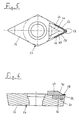
Ein weiteres Ausführungsbeispiel eines Werkzeuges 50 ist in
Fig. 5 dargestellt. Dieses Werkzeug 50 besteht aus einem
Halter 52 und einem Schneidwerkzeugeinsatz 54, die sich in
der Geometrie von den beiden zuvor beschriebenen Werkzeugen
10, 30 unterscheiden. So laufen bei dem Schneidwerkzeugeinsatz
54 die Schneidkanten 56 der PKD-Schicht 58 nicht in
einem Winkel von 35° bei einem Spitzenradius von 0,8 mm,
sondern unter einem Winkel von 55° mit einem Spitzenradius
von 0,4 mm zusammen. Ein weiterer Unterschied zu den zuvor
beschriebenen Ausführungsformen besteht darin, daß der
Schneidwerkzeugeinsatz in einer stufenförmigen Aussparung
60 in dem Halter 52 eingelötet ist. Die stufenförmige Aussparung
60 ermöglicht es, einen über den Trägerkörper 62
des Schneidwerkzeuges 54 auf der den Schneidkanten 56 abgewandten
Seite überstehenden Spanbrecher 64 vorzusehen, der
sowohl mit dem Halter 52 als auch mit dem Trägerkörper 62
verlötet ist. Wenn der Spanbrecher 64 aufgeschweißt werden
soll, empfiehlt es sich, ihn am hinteren Ende, wo er mit
dem Halter 52 zu verschweißen ist, unterseitig mit einem
flachen Vorsprung, wie mit einem Stiefelabsatz, auszubilden.
Dieser Vorsprung von z. B. etwa 1 bis 2 Zehntel
Millimeter Höhe gewährleistet bei einer ebenen Auflagefläche
am Träger und Halter einen zuverlässigen und gleichmässigen
Andruck gegen den Halter beim Schweißvorgang. Die besondere
Ausbildung des Spanbrechers 64 erfordert es, die
PKD-Schicht 58 nach dem Aufbringen auf den Trägerkörper 62
bis auf einen verbleibenden V-förmigen Winkel 66 im Bereich
der Schneidkanten 56 auszusparen. Der Spanbrecher 64 verfügt
wiederum über um etwa 45° abgeschrägte Flanken 70, die
den Schneidkanten 56 zum Brechen sich bildender Späne zugewandt
sind.Another embodiment of a
Statt der bei den gezeigten Ausführungsbeispielen vorgesehenen Spanbrecher ist auch das Aufbringen von Spanleitstufen auf den Trägerkörpern der Schneidwerkzeugeinsätze denkbar, deren Aufgabe nicht in einem Brechen der Späne auf kurze Länge, sondern in einem gezielten Ableiten entstehender Späne besteht.Instead of that provided in the exemplary embodiments shown Chip breaker is also the application of chip breakers conceivable on the carrier bodies of the cutting tool inserts, whose job is not to break up the chips short length, but arising in a targeted derivation Chips exist.
Je nach Anwendungsfall, z. B. insbesondere zum Bearbeiten festerer Werkstoffe, können die auf den Trägerkörpern aufgebrachten Schichten zur Bildung der Schneidkanten auch aus polykristallinem PKB bestehen, das auch als CBN bezeichnet wird.Depending on the application, e.g. B. especially for editing stronger materials, can be applied to the carrier bodies Layers to form the cutting edges also polycrystalline PKB exist, also known as CBN becomes.
Selbstverständlich ist es denkbar, die erfindungsgemäße Anordnung von Mitteln zur Kontrollierung der Spanbildung auch auf Vollschichtplatten, wie z. B. Wendeschneidplatten, aufzubringen, bei welchen die separaten Halter entfallen können.It is of course conceivable for the arrangement according to the invention of means to control chip formation too on full-layer boards, such as B. inserts to apply, where the separate holder can be omitted.
Die Span- und Freiwinkel können unabhängig von der Anordnung der Spanbrecher der jeweilige Einsatzart des Schneidwerkzeuges angepaßt sein. Entsprechend modifizierte Schneidwerkzeugeinsätze eignen sich sowohl zum Einsatz in Bohr-, Fräs- als auch Drehwerkzeugen.The rake and clearance angles can be independent of the arrangement the chip breaker of the respective application of the cutting tool be adjusted. Modified accordingly Cutting tool inserts are both suitable for use in Drilling, milling and turning tools.
Claims (10)
- A cutting tool, having means (22; 44; 64), disposed in the region of the chip face, for preventing uncontrolled chip formation, which means are disposed at a certain spacing from a cutting edge (26; 56) at a layer (24; 48; 58) of polycrystalline diamond (PKD) or polycrystalline boron nitride (PKB), which is applied to a substrate body (20; 46; 62), characterized in that the layer (24; 46; 58) of PKD or PKB is recessed, in the region of the means (22; 44; 64) for preventing uncontrolled chip formation, down to the substrate body (20; 46; 62), and the means (22; 44; 64) for preventing uncontrolled chip formation are applied there directly to the substrate body (20; 46; 62).
- The cutting tool of claim 1, characterized in that the means (22; 44, 64) for preventing uncontrolled chip formation are secured in materially joined fashion to the substrate body (20; 46; 62) or are secured in materially joined fashion to both the substrate body (20; 46; 62) and to a holder (12; 52) that carries the substrate body.
- The cutting tool of claim 2, characterized in that the means (22; 44, 64) for preventing uncontrolled chip formation are provided on the underside, in the rear region, with a flat protrusion having a flat lower face.
- The cutting tool of one of claims 1-3, characterized in that the recess in the layer (24; 48; 58) of PKD or PKB is produced by an erosion or evaporation method.
- The cutting tool of one of the foregoing claims, characterized in that the layer of PKD or PKB is applied to the substrate body by deposition of the cutting material in the vapor phase.
- The cutting tool of one of the foregoing claims, characterized in that the means for preventing uncontrolled chip formation are embodied as a chip guide stage.
- The cutting tool of one of claims 1-6, characterized in that the means (22; 44, 64) for preventing uncontrolled chip formation are embodied as chip breakers (22; 44; 64).
- The cutting tool of claim 7, characterized in that the flank (28), oriented toward the cutting edge (26), of the chip breaker (22) is beveled by approximately 40-50°.
- The cutting tool of one of the foregoing claims, characterized in that it is embodied as a drilling tool, milling tool or lathe tool.
- The cutting tool of one of the foregoing claims, characterized in that it is embodied as an insert (14; 42; 54) for a holder (12; 52) or as an indexable cutter plate with a plurality of cutting edges.
Priority Applications (1)
| Application Number | Priority Date | Filing Date | Title |
|---|---|---|---|
| DE20022438U DE20022438U1 (en) | 1999-01-26 | 2000-01-22 | Cutting tool with means for saving control |
Applications Claiming Priority (2)
| Application Number | Priority Date | Filing Date | Title |
|---|---|---|---|
| DE19903037A DE19903037C2 (en) | 1999-01-26 | 1999-01-26 | Cutting tool with means for chip control |
| DE19903037 | 1999-01-26 |
Publications (2)
| Publication Number | Publication Date |
|---|---|
| EP1023962A1 EP1023962A1 (en) | 2000-08-02 |
| EP1023962B1 true EP1023962B1 (en) | 2002-10-02 |
Family
ID=7895438
Family Applications (1)
| Application Number | Title | Priority Date | Filing Date |
|---|---|---|---|
| EP00101195A Expired - Lifetime EP1023962B1 (en) | 1999-01-26 | 2000-01-22 | Cutting tool with means to control the chip flow |
Country Status (4)
| Country | Link |
|---|---|
| US (1) | US6315502B1 (en) |
| EP (1) | EP1023962B1 (en) |
| DE (2) | DE19903037C2 (en) |
| ES (1) | ES2184664T3 (en) |
Families Citing this family (20)
| Publication number | Priority date | Publication date | Assignee | Title |
|---|---|---|---|---|
| US6540450B2 (en) * | 2000-11-29 | 2003-04-01 | Hayes Lemmerz International, Inc. | Tool and process for finishing a vehicle wheel surface |
| US6893330B2 (en) * | 2000-11-08 | 2005-05-17 | Hayes Lemmerz International, Inc. | Tool and process for chrome plating a vehicle wheel surface |
| US6997787B2 (en) * | 2000-11-08 | 2006-02-14 | Hayes Lemmerz International, Inc. | Process for copper free chrome plating of a vehicle wheel surface |
| CN1538890A (en) * | 2001-08-10 | 2004-10-20 | 住友电气工业株式社 | Ultra high-pressure sintered cutter with recess or groove, its manufacturing method and holding mechanism |
| JP2003127007A (en) * | 2001-08-10 | 2003-05-08 | Sumitomo Electric Ind Ltd | Throw-away tip |
| DE10216408C5 (en) * | 2002-04-12 | 2007-01-04 | Fraunhofer-Gesellschaft zur Förderung der angewandten Forschung e.V. | Method for producing a cutting tool |
| US6742970B2 (en) * | 2002-06-12 | 2004-06-01 | Kennametal Inc. | Cutting tool |
| US20050076755A1 (en) * | 2003-03-11 | 2005-04-14 | Zimmerman Michael H. | Method and apparatus for machining fiber cement |
| US7269391B2 (en) * | 2004-03-16 | 2007-09-11 | Broadcom Corporation | Tunable transceiver front end |
| JP4585243B2 (en) * | 2004-06-30 | 2010-11-24 | 株式会社アライドマテリアル | Single crystal diamond cutting tool for ultra-precision machining |
| DE202007017088U1 (en) | 2007-12-05 | 2008-04-24 | Jakob Lach Gmbh & Co. Kg | Cutting tool for the machining of workpieces |
| US9463531B2 (en) | 2009-10-23 | 2016-10-11 | Kennametal Inc. | Three-dimensional surface shaping of rotary cutting tool edges with lasers |
| WO2014155890A1 (en) * | 2013-03-29 | 2014-10-02 | 住友電工ハードメタル株式会社 | Cbn cutting tool manufacturing method and cbn cutting tool |
| DE102014207507B4 (en) | 2014-04-17 | 2021-12-16 | Kennametal Inc. | Cutting tool and method for producing a cutting tool |
| DE102014207510B4 (en) | 2014-04-17 | 2021-12-16 | Kennametal Inc. | Cutting tool and method for producing a cutting tool |
| US9643282B2 (en) | 2014-10-17 | 2017-05-09 | Kennametal Inc. | Micro end mill and method of manufacturing same |
| EP3023178B1 (en) * | 2014-11-24 | 2022-05-11 | Sandvik Intellectual Property AB | A method of grinding a parting/grooving insert and a parting/grooving insert |
| US11027339B2 (en) * | 2017-02-27 | 2021-06-08 | Kyocera Corporation | Cutting insert, cutting tool, and method of manufacturing machined product |
| US11229957B2 (en) * | 2018-10-02 | 2022-01-25 | Jakob Lach Gmbh & Co. Kg | Method for producing a cutting tool for the machining of workpieces and cutting tool |
| USD902966S1 (en) * | 2019-05-21 | 2020-11-24 | Christopher Lee Caliendo | Rhombus negative rake wood turning blade |
Family Cites Families (17)
| Publication number | Priority date | Publication date | Assignee | Title |
|---|---|---|---|---|
| US2870523A (en) * | 1956-08-10 | 1959-01-27 | Theophile J La Lime | Cutting tools |
| US2955349A (en) * | 1958-03-13 | 1960-10-11 | Gen Electric | Cutting tool |
| US4159885A (en) * | 1977-07-05 | 1979-07-03 | Schott Lawrence A | Cutting tool |
| US4189264A (en) * | 1978-09-15 | 1980-02-19 | Fansteel Inc. | Cutting insert and chip control assembly |
| US4414870A (en) * | 1981-02-19 | 1983-11-15 | Peterson Tool Company | Cutting tool |
| US4561810A (en) * | 1981-12-16 | 1985-12-31 | General Electric Company | Bi-level cutting insert |
| US4714385A (en) * | 1986-02-27 | 1987-12-22 | General Electric Company | Polycrystalline diamond and CBN cutting tools |
| US4856942A (en) * | 1988-07-19 | 1989-08-15 | Gte Valenite Corporation | Polygonal cutting insert |
| US4854784A (en) * | 1988-10-19 | 1989-08-08 | Kennametal Inc. | Diamond tipped chip control insert |
| CA2036930C (en) * | 1990-02-27 | 1996-01-09 | Hitoshi Fukuoka | Cutting insert |
| SE500310C2 (en) * | 1990-12-03 | 1994-05-30 | Sandvik Ab | Cutting and cutting tool |
| SE502199C2 (en) * | 1990-12-19 | 1995-09-11 | Sandvik Ab | Drill inserts with inclined front cutting edges and drilling tools for this |
| US5193948A (en) * | 1991-12-16 | 1993-03-16 | Gte Valenite Corporation | Chip control inserts with diamond segments |
| US5405711A (en) * | 1993-09-20 | 1995-04-11 | Valenite Inc. | Indexable inserts with polycrystalline cutting edge |
| SE509362C2 (en) * | 1994-03-18 | 1999-01-18 | Sandvik Ab | Diamond coated body |
| DE69517502T2 (en) * | 1995-03-10 | 2000-10-19 | Valenite Inc | High-speed cutting insert with chip breaker |
| US6146064A (en) * | 1999-01-12 | 2000-11-14 | Tool Flo Manufacturing, Inc. | Cutting insert with improved chip control |
-
1999
- 1999-01-26 DE DE19903037A patent/DE19903037C2/en not_active Expired - Fee Related
-
2000
- 2000-01-22 ES ES00101195T patent/ES2184664T3/en not_active Expired - Lifetime
- 2000-01-22 EP EP00101195A patent/EP1023962B1/en not_active Expired - Lifetime
- 2000-01-22 DE DE50000573T patent/DE50000573D1/en not_active Expired - Lifetime
- 2000-01-27 US US09/492,948 patent/US6315502B1/en not_active Expired - Lifetime
Also Published As
| Publication number | Publication date |
|---|---|
| DE19903037C2 (en) | 2003-12-04 |
| DE50000573D1 (en) | 2002-11-07 |
| EP1023962A1 (en) | 2000-08-02 |
| DE19903037A1 (en) | 2000-08-03 |
| US6315502B1 (en) | 2001-11-13 |
| ES2184664T3 (en) | 2003-04-16 |
Similar Documents
| Publication | Publication Date | Title |
|---|---|---|
| EP1023962B1 (en) | Cutting tool with means to control the chip flow | |
| DE2840610C2 (en) | ||
| DE3037097C2 (en) | Solid drilling tools, especially twist drills | |
| DE19724319C1 (en) | Influencing characteristics of chip flow from tool surfaces | |
| EP1023961B1 (en) | Cutting tool | |
| EP2067552B1 (en) | Cutting tool for machining a workpiece | |
| EP3385014B1 (en) | Drilling tool and method for manufacturing a drilling tool for the machining of workpieces | |
| DE10002108C2 (en) | Removable chip breaker for a cutting insert | |
| DE102015223484B4 (en) | Cutting tool and method of making same | |
| WO2013142885A1 (en) | Cutting insert | |
| DE3020929C2 (en) | Tungsten carbide cutter tip coated with hard material and process for its manufacture | |
| EP0696942B1 (en) | Polygonal cutting insert | |
| EP1401601B2 (en) | Cutting device | |
| AT9431U1 (en) | CUTTING BOARD | |
| EP2200775B1 (en) | Reamer | |
| EP0537476B1 (en) | Milling head | |
| DE112019003627T5 (en) | CUTTING INSERT, CUTTING TOOL AND METHOD FOR MANUFACTURING A MACHINED PRODUCT | |
| DE102019117799B4 (en) | Cutting tool with asymmetrical teeth with cutting particles | |
| EP3892407A1 (en) | Tool for the machining of non-metallic materials | |
| AT500864B1 (en) | INSERTION PLATE FOR ISO CLAMP HOLDER | |
| WO2004050296A1 (en) | Cutting plate | |
| EP0595763B1 (en) | Cutter bar with a high wear resistance and method of making it | |
| EP3199272A1 (en) | Cutting tool for machining of a workpiece | |
| DE112021002885T5 (en) | CUTTING INSERT, CUTTING TOOL AND METHOD OF MAKING A MACHINED PRODUCT | |
| WO2014190363A1 (en) | Cutting insert made of hard metal or cermet for rotary machining |
Legal Events
| Date | Code | Title | Description |
|---|---|---|---|
| PUAI | Public reference made under article 153(3) epc to a published international application that has entered the european phase |
Free format text: ORIGINAL CODE: 0009012 |
|
| AK | Designated contracting states |
Kind code of ref document: A1 Designated state(s): DE ES FR GB IT SE |
|
| AX | Request for extension of the european patent |
Free format text: AL;LT;LV;MK;RO;SI |
|
| 17P | Request for examination filed |
Effective date: 20010112 |
|
| AKX | Designation fees paid |
Free format text: DE ES FR GB IT SE |
|
| GRAG | Despatch of communication of intention to grant |
Free format text: ORIGINAL CODE: EPIDOS AGRA |
|
| GRAG | Despatch of communication of intention to grant |
Free format text: ORIGINAL CODE: EPIDOS AGRA |
|
| 17Q | First examination report despatched |
Effective date: 20020204 |
|
| GRAG | Despatch of communication of intention to grant |
Free format text: ORIGINAL CODE: EPIDOS AGRA |
|
| GRAH | Despatch of communication of intention to grant a patent |
Free format text: ORIGINAL CODE: EPIDOS IGRA |
|
| GRAH | Despatch of communication of intention to grant a patent |
Free format text: ORIGINAL CODE: EPIDOS IGRA |
|
| GRAA | (expected) grant |
Free format text: ORIGINAL CODE: 0009210 |
|
| AK | Designated contracting states |
Kind code of ref document: B1 Designated state(s): DE ES FR GB IT SE |
|
| REG | Reference to a national code |
Ref country code: GB Ref legal event code: FG4D Free format text: NOT ENGLISH |
|
| REF | Corresponds to: |
Ref document number: 50000573 Country of ref document: DE Date of ref document: 20021107 |
|
| GBT | Gb: translation of ep patent filed (gb section 77(6)(a)/1977) |
Effective date: 20030130 |
|
| REG | Reference to a national code |
Ref country code: ES Ref legal event code: FG2A Ref document number: 2184664 Country of ref document: ES Kind code of ref document: T3 |
|
| ET | Fr: translation filed | ||
| PLBE | No opposition filed within time limit |
Free format text: ORIGINAL CODE: 0009261 |
|
| STAA | Information on the status of an ep patent application or granted ep patent |
Free format text: STATUS: NO OPPOSITION FILED WITHIN TIME LIMIT |
|
| 26N | No opposition filed |
Effective date: 20030703 |
|
| REG | Reference to a national code |
Ref country code: DE Ref legal event code: R082 Ref document number: 50000573 Country of ref document: DE Representative=s name: STOFFREGEN, HANS-HERBERT, DIPL.-PHYS. DR.RER.N, DE |
|
| REG | Reference to a national code |
Ref country code: FR Ref legal event code: PLFP Year of fee payment: 17 |
|
| PGFP | Annual fee paid to national office [announced via postgrant information from national office to epo] |
Ref country code: IT Payment date: 20160127 Year of fee payment: 17 Ref country code: ES Payment date: 20160112 Year of fee payment: 17 |
|
| PGFP | Annual fee paid to national office [announced via postgrant information from national office to epo] |
Ref country code: SE Payment date: 20160120 Year of fee payment: 17 Ref country code: FR Payment date: 20160121 Year of fee payment: 17 Ref country code: GB Payment date: 20160120 Year of fee payment: 17 |
|
| GBPC | Gb: european patent ceased through non-payment of renewal fee |
Effective date: 20170122 |
|
| REG | Reference to a national code |
Ref country code: FR Ref legal event code: ST Effective date: 20170929 |
|
| PG25 | Lapsed in a contracting state [announced via postgrant information from national office to epo] |
Ref country code: FR Free format text: LAPSE BECAUSE OF NON-PAYMENT OF DUE FEES Effective date: 20170131 |
|
| PG25 | Lapsed in a contracting state [announced via postgrant information from national office to epo] |
Ref country code: GB Free format text: LAPSE BECAUSE OF NON-PAYMENT OF DUE FEES Effective date: 20170122 Ref country code: SE Free format text: LAPSE BECAUSE OF NON-PAYMENT OF DUE FEES Effective date: 20170123 |
|
| PG25 | Lapsed in a contracting state [announced via postgrant information from national office to epo] |
Ref country code: IT Free format text: LAPSE BECAUSE OF NON-PAYMENT OF DUE FEES Effective date: 20170122 |
|
| PG25 | Lapsed in a contracting state [announced via postgrant information from national office to epo] |
Ref country code: ES Free format text: LAPSE BECAUSE OF NON-PAYMENT OF DUE FEES Effective date: 20170123 |
|
| REG | Reference to a national code |
Ref country code: ES Ref legal event code: FD2A Effective date: 20181113 |
|
| PGFP | Annual fee paid to national office [announced via postgrant information from national office to epo] |
Ref country code: DE Payment date: 20190129 Year of fee payment: 20 |
|
| REG | Reference to a national code |
Ref country code: DE Ref legal event code: R071 Ref document number: 50000573 Country of ref document: DE |