EP1020979A2 - Nachreglersteuerschaltung für einen Mehrfachausgansschaltnetzteil - Google Patents
Nachreglersteuerschaltung für einen Mehrfachausgansschaltnetzteil Download PDFInfo
- Publication number
- EP1020979A2 EP1020979A2 EP00650002A EP00650002A EP1020979A2 EP 1020979 A2 EP1020979 A2 EP 1020979A2 EP 00650002 A EP00650002 A EP 00650002A EP 00650002 A EP00650002 A EP 00650002A EP 1020979 A2 EP1020979 A2 EP 1020979A2
- Authority
- EP
- European Patent Office
- Prior art keywords
- control circuit
- output
- regulation control
- post regulation
- voltage
- Prior art date
- Legal status (The legal status is an assumption and is not a legal conclusion. Google has not performed a legal analysis and makes no representation as to the accuracy of the status listed.)
- Withdrawn
Links
Images


Classifications
-
- H—ELECTRICITY
- H02—GENERATION; CONVERSION OR DISTRIBUTION OF ELECTRIC POWER
- H02M—APPARATUS FOR CONVERSION BETWEEN AC AND AC, BETWEEN AC AND DC, OR BETWEEN DC AND DC, AND FOR USE WITH MAINS OR SIMILAR POWER SUPPLY SYSTEMS; CONVERSION OF DC OR AC INPUT POWER INTO SURGE OUTPUT POWER; CONTROL OR REGULATION THEREOF
- H02M1/00—Details of apparatus for conversion
- H02M1/38—Means for preventing simultaneous conduction of switches
-
- H—ELECTRICITY
- H02—GENERATION; CONVERSION OR DISTRIBUTION OF ELECTRIC POWER
- H02M—APPARATUS FOR CONVERSION BETWEEN AC AND AC, BETWEEN AC AND DC, OR BETWEEN DC AND DC, AND FOR USE WITH MAINS OR SIMILAR POWER SUPPLY SYSTEMS; CONVERSION OF DC OR AC INPUT POWER INTO SURGE OUTPUT POWER; CONTROL OR REGULATION THEREOF
- H02M3/00—Conversion of dc power input into dc power output
- H02M3/22—Conversion of dc power input into dc power output with intermediate conversion into ac
- H02M3/24—Conversion of dc power input into dc power output with intermediate conversion into ac by static converters
- H02M3/28—Conversion of dc power input into dc power output with intermediate conversion into ac by static converters using discharge tubes with control electrode or semiconductor devices with control electrode to produce the intermediate ac
- H02M3/325—Conversion of dc power input into dc power output with intermediate conversion into ac by static converters using discharge tubes with control electrode or semiconductor devices with control electrode to produce the intermediate ac using devices of a triode or a transistor type requiring continuous application of a control signal
- H02M3/335—Conversion of dc power input into dc power output with intermediate conversion into ac by static converters using discharge tubes with control electrode or semiconductor devices with control electrode to produce the intermediate ac using devices of a triode or a transistor type requiring continuous application of a control signal using semiconductor devices only
- H02M3/33561—Conversion of dc power input into dc power output with intermediate conversion into ac by static converters using discharge tubes with control electrode or semiconductor devices with control electrode to produce the intermediate ac using devices of a triode or a transistor type requiring continuous application of a control signal using semiconductor devices only having more than one ouput with independent control
Definitions
- the present invention relates to a post regulation control circuit for a switch mode power supply (SMPS) with multiple outputs, said circuit being of the phase modulation trailing edge synchronisation type having a ramp generator and a triggering mechanism.
- SMPS switch mode power supply
- switch mode power supplies take electrical power from a source as an input voltage and deliver electrical power to multiple loads.
- the invention is particularly directed to isolated or non-isolated single-ended or double-ended converters.
- they can be buck-derived isolated or non-isolated SMPS which take power from a source at a voltage Vin , and deliver power to a load, at a voltage Vo .
- the output voltage is regulated in order to guarantee that a constant voltage is applied to the load even if the input voltage Vin or the output current lo or both vary.
- Magnetic amplifier output regulators have been used as a means for regulating more than one output of a switching supply. They are particularly suitable for currents of 1 amp to more than 20 or 30 amps, though they have been used where tight regulation and efficiency are extremely important at lower current ratings. They are efficient in that they provide extremely precise regulation of each independent output and are simple and reliable. Closely regulated outputs can be obtained using a simple control circuit.
- the magnetic amplifiers tend to be bulky and expensive. Moreover they can be lossy particularly if the switching frequency is high. Minimum delay times do cause duty cycle losses, and reduce the maximum achievable output voltage for the auxiliary outputs.
- a typical magnetic amplifier and the design of such high frequency magnetic amplifier output regulators is described in an application guide produced by Allied Signal Inc. and entitled 'Design of High Frequency Mag Amp Regulators Using Metglas' (see 1997 Allied Signal Inc. R697/1.5M)
- Magnetic amplifier regulators have problems in that because they have to withstand the maximum input voltages during a short circuit condition, they are effectively over-designed, typically by a factor of two which increases the cost and size of the power supply. Secondly, they are inherently leading edge modulators so that you can only approach a certain maximum duty cycle limited by the minimum delay and the magnetic BH loop characteristics of the magnetic amplifier core. This forces an increase in the size of the main transformer as well as the output inductor resulting in high overall system costs.
- one or more buck converters can be connected to the main output Vo1 and deliver independently regulated outputs. Good results in terms of efficiency can be achieved at the expense of increased output noise at the main output Vo1 . Additionally the pulsating input current into the buck stage causes a high ripple current stress of the output filter capacitor of the main output.
- the buck converter can be replaced by a current-fed converter with a continuous input current. The output noise problems can be solved, but new problems are introduced , for example, poor boost switch utilisation.
- auxiliary outputs are not directly derived from the main output but from the pulsating voltage at the secondary of the transformer.
- Regulation of the auxiliary output is achieved by phase modulation in combination with a controlled rectifier.
- Leading-edge pulse width modulation means that at the beginning of the power cycle the primary current equals the reflected sum of the output currents. After the controlled forward rectifier is turned off the primary current drops to a value equal to the reflected main output current. This shape of the primary current is no longer compatible with primary-peak-current-mode-control (PPCMC) as the most popular SMPS control scheme. Voltage mode control or average current mode control has to be used, each with its own set of problems.
- the post regulator control circuit ensures that the trailing edges of the power pulses into the main and auxiliary outputs are synchronised.
- a typical example of such an approach is a secondary side post regulator for AC/DC and DC/DC multiple output converters manufactured by Cherry Semiconductor Corporation and identified under the product No. CS5101 and described in a data sheet of the same title, copyright ⁇ 1995 Cherry Semiconductor Corporation.
- the post regulator control circuit ensures that the trailing edges of main and auxiliary outputs are synchronised. A ramp is generated, and triggered at the start of each power cycle. Depending on the error of the output voltage of the auxiliary output, a delay between the start of the main power cycle and the turn-on of the synchronous switch is generated.
- Trailing-edge phase modulation between the main output and the auxiliary output is achieved. While good efficiency figures, good regulation and low output noise can be achieved the scheme shares one disadvantage with magnetic amplifiers. Inherently there will be control circuit propagation delays between the detection of the start of the power cycle to turn-on of the controlled forward rectifier. This results in a duty cycle loss of the auxiliary output with respect to the main output. Since these propagation delays are inherent to the control circuit, and constant versus the switching frequency of the SMPS, the problem gets worse at higher switching frequencies.
- trailing edge synchronisation In this specification we have referred to trailing edge synchronisation. However, when talking about modulation people skilled in the art may refer to this as leading edge modulation. Thus, in Figure 3 the trailing edges of Vrect1 and Vrect2 are synchronised and similarly it is correct to say their leading edges are modulated.
- the present invention is directed towards providing an improved construction of a post regulation control circuit for a switch mode power supply with multiple outputs of a phase modulation type having trailing edge synchronisation, a ramp generator and a triggering mechanism.
- a post regulation control circuit for a switch mode power supply with multiple outputs of the phase modulation type with trailing edge synchronisation having a ramp generator and a triggering mechanism, characterised in that the end of the power cycle is detected and triggers the ramp generator.
- a synchronous pulse generator is used to detect the end of the power cycle and trigger the ramp generator.
- a synchronous pulse generator is a particularly suitable way of carrying out the present invention.
- the synchronous pulse generator triggers a flip-flop as well as triggering the ramp generator.
- Gate signals can be provided for a control forward generator and if present for a control forward rectifier and if present for a control forward control free-wheel rectifier.
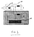
- FIG. 1 a switch mode power supply a transformer isolated single-ended buck converter indicated generally by the reference numeral 10 which provides a main output voltage Vo1 which is regulated by a pulse width modulator (PWM) 11 sited on the primary side of the converter 10.
- PWM pulse width modulator
- a plurality of auxiliary outputs, in this case three are shown, and one of the outputs is identified by the reference letter N can be derived by tapping from the secondary side of the converter 10, the output will be a pulsating voltage and it is in turn regulated by a post regulator control circuit 12.
- the output of the converter 10 comprises a pair of uncontrolled rectifiers formed from diodes D1a and D1b and filtering elements L1 and C1.
- the main output voltage Vo1 is sensed at 13 and is fed back to the main pulse width modulator 11.
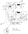
- the post regulator control circuit 12 comprises a synchronous pulse generator 1 feeding a ramp generator 2 which in turn feeds a comparator 4 feeding a flip-flop 5 which is also fed directly from the synchronous pulse generator 1.
- the flip-flop 5 feeds through two delay devices 6 and 8, drivers 7 and 9 respectively.
- One driver 7 feeds a controllable switch in this case a MOSFET S2a and the other driver 9 feeds a further controllable switch provided by a MOSFET S2b.
- Suitable filtering elements L2 and C2 are included to the auxiliary output stage.
- the auxiliary output stage again feeds back through an error amplifier EA1 to sense the output voltage of the auxiliary output Vo2 and to develop a signal reflecting the error of the output voltage.
- the output voltage is fed from the error amplifier EA1 through an inverter 3 to the comparator 4.
- the output voltage Vo1 is sensed and the duty cycle is adjusted by the pulse width modulator 11 to maintain the desired level of output voltage Vo1 in a closed-loop fashion as is conventional.
- the main power cycle with the duration d1*Ts spans from time point t0 to t2 .
- the synchronous pulse generator 1 detects the end of each power cycle by detecting in this embodiment the falling edge of the voltage vsectp . It will be appreciated that the voltage vrect1 could equally well be detected.
- the synchronous pulse generator 1 feeds the flip-flop 5, while simultaneously triggering the ramp generator 2. As can be seen from Figure 3 the ramp voltage vramp is reset to its initial value at the end of each power cycle and starts ramping up towards its final value preferably in a linear fashion.
- the flip-flop 5 feeds through the delay elements 6 and 8 to the drivers 7 and 9 to amplify the outputs of the flip-flop 5 and to provide driving signals to the switch at S2a and S2b, which in turn gives the voltage output Vo2.
- error amplifier EA1 senses the output voltage Vo2 and develops a signal reflecting the error of the output voltage.
- the output voltage of error amplifier EA1 is low if the output voltage Vo2 is above its desired value.
- Inverter 3 derives a voltage vcomp as can be seen from Figure 3 which is high if the output voltage Vo2 is above its desired value.
- the output of comparator 4 will swing from low to high as soon as the ramp voltage vramp hits the compare voltage vcomp .
- a low-to-high transition of the output of comparator 4 will set the flip-flop 5 leading to subsequent turn-on of the forward switch S2a.
- the switch S2a is on the power cycle for the auxiliary output is initiated. This happens at time point t1 .
- ramp generator While the ramp generator has been triggered at the end of the power cycle, it is envisaged that there could be a delay between the end of the power cycle and ramp generation. This would mean that the ramp generator would only start operating at a time someway into the freewheeling cycle. This time would be dependent on the delay introduced.
- the ramp generator might supply a decaying voltage.
- any digital or analog implementation of the synchronous pulse generator is possible, for example, a MOSFET switch with resistor and capacitor components suitably arranged could be used to detect the falling edge and trigger the ramp generator.
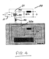
- FIG. 4 there is illustrated a circuit diagram of a converter indicated generally by the reference numeral 20 in which parts similar to those described with reference to the previous drawings are identified by the same reference numerals. Indeed everything in converter 20 is identical to the converter as illustrated in Figure 1, except that there is provided a transformer indicated generally by the reference numeral 21 having a plurality of secondary coils 22, each of which is dedicated to an auxiliary output
- the switch S2a is a bi-directional switch which is directly connected to the secondary coil 22 of the transformer. It will be appreciated that if the switch S2a is not a bi-directional switch, for example if it is a MOSFET which cannot block a bipolar voltage an additional diode could be used in series with the switch S2a and this could be a dedicated diode, or indeed for example the diode D1a.
- FIG. 5 there is illustrated a block diagram of a converter for current mode control components similar to those previously described and identified by the same reference numerals.
- the ramp generation is provided by the inductor L2 which will be amplified and often can be level shifted.
- the inductor L2 provides a natural ramp current riding on a DC level which can be used for control.
- the current in L2 is sensed and is converted into a voltage in a tran-impedance block 20.
- the reason for using the delay elements is to prevent cross conduction of MOSFETS, but such delay elements are optional and can be implemented in an adaptive or non-adaptive fashion.
- driver 9 as illustrated in Figure 2 is optional and will only be required, If, for example, the switch S2b is a controllable switch and not, for example, a diode.
- the invention can be applied to a wide variety of applications. It can be used in both single-ended and double-ended rectification applications regardless of the type and arrangement of rectifiers used in the main output. It will also be appreciated that, for example, the diodes in the main circuit can be replaced by synchronous rectifiers to boost the power conversion efficiencies and further instead of MOSFETS, the diodes can be used.
- control mode of the post regulation control circuit could be easily changed to current mode control resulting in improved dynamic performance.
- the flip-flop 5 as, for example, in the circuit of Figure 2 is not required in low-noise environments and would thus be optional.
- the output of the comparator 4 in the circuit of Figure 2 could be fed into the delay element 6, and inverted into the delay element 8.
- the flip-flop 5 improves the performance of the post regulation control circuit in noisy environments.
Landscapes
- Engineering & Computer Science (AREA)
- Power Engineering (AREA)
- Dc-Dc Converters (AREA)
- Control Of Eletrric Generators (AREA)
Applications Claiming Priority (2)
| Application Number | Priority Date | Filing Date | Title |
|---|---|---|---|
| IE990019 | 1999-01-12 | ||
| IE990019 | 1999-01-12 |
Publications (2)
| Publication Number | Publication Date |
|---|---|
| EP1020979A2 true EP1020979A2 (de) | 2000-07-19 |
| EP1020979A3 EP1020979A3 (de) | 2001-09-26 |
Family
ID=11041982
Family Applications (1)
| Application Number | Title | Priority Date | Filing Date |
|---|---|---|---|
| EP00650002A Withdrawn EP1020979A3 (de) | 1999-01-12 | 2000-01-12 | Nachreglersteuerschaltung für einen Mehrfachausgansschaltnetzteil |
Country Status (3)
| Country | Link |
|---|---|
| US (1) | US6222747B1 (de) |
| EP (1) | EP1020979A3 (de) |
| IE (2) | IE20000021A1 (de) |
Cited By (1)
| Publication number | Priority date | Publication date | Assignee | Title |
|---|---|---|---|---|
| WO2003043166A1 (en) * | 2001-11-12 | 2003-05-22 | Power-One, Inc. | Leading edge modulator for post regulation of multiple output voltage power supplies |
Families Citing this family (6)
| Publication number | Priority date | Publication date | Assignee | Title |
|---|---|---|---|---|
| US6490179B1 (en) | 2001-10-31 | 2002-12-03 | Innoveta Technologies | Post-regulated power supply |
| US6703817B2 (en) | 2002-03-07 | 2004-03-09 | Lambda Electronics, Inc. | Pulse width modulated power conversion apparatus and methods using capacitor-charge feedback |
| ITTO20020545A1 (it) * | 2002-06-21 | 2003-12-22 | St Microelectronics Srl | Circuito di controllo in modalita' pwm per la post-regolazione di alimentatori a commutazione a molte uscite |
| US6912138B2 (en) | 2002-09-03 | 2005-06-28 | Artesyn Technologies, Inc. | Synchronous rectifier control circuit |
| JP4715429B2 (ja) * | 2005-09-29 | 2011-07-06 | 富士電機システムズ株式会社 | 交直変換回路 |
| US10033288B2 (en) * | 2016-05-25 | 2018-07-24 | Dialog Semiconductor Inc. | Auxiliary load application for increasing data rate of messages or for increasing the response speed to transmitted messages in a flyback converter |
Citations (3)
| Publication number | Priority date | Publication date | Assignee | Title |
|---|---|---|---|---|
| EP0605752A2 (de) * | 1993-01-05 | 1994-07-13 | Yokogawa Electric Corporation | Schaltnetzteil |
| US5528480A (en) * | 1994-04-28 | 1996-06-18 | Elonex Technologies, Inc. | Highly efficient rectifying and converting circuit for computer power supplies |
| US5841313A (en) * | 1995-08-30 | 1998-11-24 | Cherry Semiconductor Corporation | Switch with programmable delay |
Family Cites Families (7)
| Publication number | Priority date | Publication date | Assignee | Title |
|---|---|---|---|---|
| JPH07118918B2 (ja) | 1989-01-26 | 1995-12-18 | 三菱電機株式会社 | Dc/dc電源装置 |
| US5003454A (en) * | 1990-01-09 | 1991-03-26 | North American Philips Corporation | Power supply with improved power factor correction |
| US5428267A (en) | 1992-07-09 | 1995-06-27 | Premier Power Systems, Inc. | Regulated DC power supply |
| EP0602835B1 (de) | 1992-12-15 | 1996-05-01 | AT&T Corp. | Spannungssteuerschaltungen |
| US5615093A (en) | 1994-08-05 | 1997-03-25 | Linfinity Microelectronics | Current synchronous zero voltage switching resonant topology |
| US5862042A (en) | 1997-10-03 | 1999-01-19 | Lucent Technologies, Inc. | Multiple output DC to DC converter |
| US6091233A (en) * | 1999-01-14 | 2000-07-18 | Micro Linear Corporation | Interleaved zero current switching in a power factor correction boost converter |
-
2000
- 2000-01-12 EP EP00650002A patent/EP1020979A3/de not_active Withdrawn
- 2000-01-12 US US09/481,403 patent/US6222747B1/en not_active Expired - Fee Related
- 2000-01-12 IE IE20000021A patent/IE20000021A1/en not_active IP Right Cessation
- 2000-01-12 IE IE20000022A patent/IES20000022A2/en not_active IP Right Cessation
Patent Citations (3)
| Publication number | Priority date | Publication date | Assignee | Title |
|---|---|---|---|---|
| EP0605752A2 (de) * | 1993-01-05 | 1994-07-13 | Yokogawa Electric Corporation | Schaltnetzteil |
| US5528480A (en) * | 1994-04-28 | 1996-06-18 | Elonex Technologies, Inc. | Highly efficient rectifying and converting circuit for computer power supplies |
| US5841313A (en) * | 1995-08-30 | 1998-11-24 | Cherry Semiconductor Corporation | Switch with programmable delay |
Non-Patent Citations (1)
| Title |
|---|
| COOKE P: "CONTROL LOOP INTERACTIONS FOR SECONDARY SIDE POST REGULATORS" APEC '98. 13TH ANNUAL APPLIED POWER ELECTRONICS CONFERENCE AND EXPOSITION. ANAHEIM, CA, FEBR. 15 - 19, 1998, ANNUAL APPLIED POWER ELECTRONICS CONFERENCE, NEW YORK, NY: IEEE, US, vol. 1, 15 February 1998 (1998-02-15), pages 369-376, XP000873683 ISBN: 0-7803-4341-7 * |
Cited By (1)
| Publication number | Priority date | Publication date | Assignee | Title |
|---|---|---|---|---|
| WO2003043166A1 (en) * | 2001-11-12 | 2003-05-22 | Power-One, Inc. | Leading edge modulator for post regulation of multiple output voltage power supplies |
Also Published As
| Publication number | Publication date |
|---|---|
| IES20000022A2 (en) | 2000-09-20 |
| US6222747B1 (en) | 2001-04-24 |
| IE20000021A1 (en) | 2000-09-20 |
| EP1020979A3 (de) | 2001-09-26 |
Similar Documents
| Publication | Publication Date | Title |
|---|---|---|
| US6246592B1 (en) | Unique power supply architecture with cascaded converters for large input-to-output step-down ratio | |
| US5999433A (en) | Half-bridge DC to DC converter with low output current ripple | |
| US5886508A (en) | Multiple output voltages from a cascaded buck converter topology | |
| US5072171A (en) | High efficiency power converter employing a synchronized switching system | |
| US6831847B2 (en) | Synchronous rectifier drive circuit and power supply including same | |
| KR100519440B1 (ko) | 소프트펄스폭변조스위칭을이용한위상스태거방식의풀-브리지변환기 | |
| US6885176B2 (en) | PWM control circuit for the post-adjustment of multi-output switching power supplies | |
| US5654881A (en) | Extended range DC-DC power converter circuit | |
| US6788554B2 (en) | Switched mode power converter having synchronous rectification and secondary side post regulation | |
| US9041372B2 (en) | Wide output voltage range switching power converter | |
| US20040022075A1 (en) | Full-wave coupled inductor power converter | |
| US4847742A (en) | Multi-channel inverter circuit | |
| US20210305902A1 (en) | Welding power supply with extended voltage characteristic | |
| JPS5931245B2 (ja) | 電源電圧制御型増幅器 | |
| JP2003153537A (ja) | 後調節電源装置 | |
| US4138715A (en) | Resonant switching converter | |
| US11843316B2 (en) | Wide-voltage-range DC-DC converters | |
| US6744647B2 (en) | Parallel connected converters apparatus and methods using switching cycle with energy holding state | |
| US7388761B1 (en) | High efficiency parallel post regulator for wide range input DC/DC converter | |
| US6222747B1 (en) | Post regulation control circuit for a switch mode power supply with multiple outputs | |
| EP0966091A2 (de) | Gleichstrom-Gleichstromwandler mit integriertem magnetischem Leistungstransformator | |
| US6912138B2 (en) | Synchronous rectifier control circuit | |
| Chen et al. | New multi-output switching converters with MOSFET-rectifier post regulators | |
| US6661209B2 (en) | Leading edge modulator for post regulation of multiple output voltage power supplies | |
| EP0942520A2 (de) | Gleichstrom-Gleichstromwandler |
Legal Events
| Date | Code | Title | Description |
|---|---|---|---|
| PUAI | Public reference made under article 153(3) epc to a published international application that has entered the european phase |
Free format text: ORIGINAL CODE: 0009012 |
|
| AK | Designated contracting states |
Kind code of ref document: A2 Designated state(s): AT BE CH CY DE DK ES FI FR GB GR IE IT LI LU MC NL PT SE |
|
| AX | Request for extension of the european patent |
Free format text: AL;LT;LV;MK;RO;SI |
|
| RIN1 | Information on inventor provided before grant (corrected) |
Inventor name: RINNE, KARL Inventor name: O SUILLEABHAIN, LIAM |
|
| PUAL | Search report despatched |
Free format text: ORIGINAL CODE: 0009013 |
|
| AK | Designated contracting states |
Kind code of ref document: A3 Designated state(s): AT BE CH CY DE DK ES FI FR GB GR IE IT LI LU MC NL PT SE |
|
| AX | Request for extension of the european patent |
Free format text: AL;LT;LV;MK;RO;SI |
|
| AKX | Designation fees paid | ||
| REG | Reference to a national code |
Ref country code: DE Ref legal event code: 8566 |
|
| STAA | Information on the status of an ep patent application or granted ep patent |
Free format text: STATUS: THE APPLICATION IS DEEMED TO BE WITHDRAWN |
|
| 18D | Application deemed to be withdrawn |
Effective date: 20020327 |