EP1019935B1 - Row electrode anodization - Google Patents
Row electrode anodization Download PDFInfo
- Publication number
- EP1019935B1 EP1019935B1 EP98942358A EP98942358A EP1019935B1 EP 1019935 B1 EP1019935 B1 EP 1019935B1 EP 98942358 A EP98942358 A EP 98942358A EP 98942358 A EP98942358 A EP 98942358A EP 1019935 B1 EP1019935 B1 EP 1019935B1
- Authority
- EP
- European Patent Office
- Prior art keywords
- row electrode
- present
- field emission
- row
- electrode
- Prior art date
- Legal status (The legal status is an assumption and is not a legal conclusion. Google has not performed a legal analysis and makes no representation as to the accuracy of the status listed.)
- Expired - Lifetime
Links
Images


Classifications
-
- H—ELECTRICITY
- H01—ELECTRIC ELEMENTS
- H01J—ELECTRIC DISCHARGE TUBES OR DISCHARGE LAMPS
- H01J1/00—Details of electrodes, of magnetic control means, of screens, or of the mounting or spacing thereof, common to two or more basic types of discharge tubes or lamps
- H01J1/02—Main electrodes
- H01J1/30—Cold cathodes, e.g. field-emissive cathode
-
- H—ELECTRICITY
- H01—ELECTRIC ELEMENTS
- H01J—ELECTRIC DISCHARGE TUBES OR DISCHARGE LAMPS
- H01J9/00—Apparatus or processes specially adapted for the manufacture, installation, removal, maintenance of electric discharge tubes, discharge lamps, or parts thereof; Recovery of material from discharge tubes or lamps
- H01J9/02—Manufacture of electrodes or electrode systems
- H01J9/14—Manufacture of electrodes or electrode systems of non-emitting electrodes
- H01J9/148—Manufacture of electrodes or electrode systems of non-emitting electrodes of electron emission flat panels, e.g. gate electrodes, focusing electrodes or anode electrodes
-
- H—ELECTRICITY
- H01—ELECTRIC ELEMENTS
- H01J—ELECTRIC DISCHARGE TUBES OR DISCHARGE LAMPS
- H01J29/00—Details of cathode-ray tubes or of electron-beam tubes of the types covered by group H01J31/00
- H01J29/46—Arrangements of electrodes and associated parts for generating or controlling the ray or beam, e.g. electron-optical arrangement
- H01J29/467—Control electrodes for flat display tubes, e.g. of the type covered by group H01J31/123
-
- H—ELECTRICITY
- H01—ELECTRIC ELEMENTS
- H01J—ELECTRIC DISCHARGE TUBES OR DISCHARGE LAMPS
- H01J3/00—Details of electron-optical or ion-optical arrangements common to two or more basic types of discharge tubes or lamps
- H01J3/02—Electron guns
- H01J3/021—Electron guns using a field emission, photo emission, or secondary emission electron source
- H01J3/022—Electron guns using a field emission, photo emission, or secondary emission electron source with microengineered cathode, e.g. Spindt-type
Definitions
- EP-A-0364964 structures and methods of manufacture for field emission cathodes having cathode tips of minute size are disclosed.
- a matrix addressed flat panel display is disclosed and includes a lower planar array of spaced apart, parallel, electrically conductive leads and a matrix array of field emission cathodes connected to and extending up from the lower planar array of electrically conductive leads.
- JP 5,094,760 provides a field emission component (FEC) having an oxide film in uniform thickness as a resistance layer between a cathode electrode and an emitter.
- FEC field emission component
- the present invention provides a row electrode formation method which is less susceptible to damage during subsequent process steps utilized during the fabrication of the field emission display device.
- the present invention provides a row electrode formation method for use in a field emission display device wherein the row electrode reduces the occurrence of row to column shorts.
- the present invention provides a row electrode formation method which improves reliability and yield.
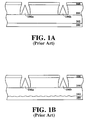
- Prior Art Figure 1B is a side sectional view illustrating a defect-containing conventional field emission display structure.
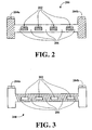
- FIG. 3 a top plan view of row electrode 200 of Figure 2 is shown after subjecting row electrode to an anodization process.
- selectively masked row electrode 200 is subjected to an anodization process using, for example, a citric acid solution to accomplish the anodization process.
- row electrode 200 is thereby anodized at the unmasked regions 206, and is not anodized at regions 202, 204a, and 204b.
- those surface areas of row electrode 200 which need to be conductive e.g. sub-pixel and pad areas
- those surface areas of row electrode 200 which do not need to be conductive are anodized.
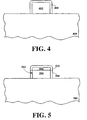
- the tantalum-clad portions of row electrode 502 (e.g. the top surface 506 of row electrode 502) are coated with Ta 2 O 5 510.
- row electrode 502 is subjected to the above-described anodization process at those surface areas of row electrode 502 which do not need to be conductive (e.g. areas other than sub-pixel and pad areas). Additionally, in this example of the present invention, in which the row electrode has exposed regions of both aluminum and tantalum, anodization of the aluminum and the tantalum is achieved concurrently.
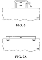
- the present embodiment then deposits a resistor layer 706 over portions of row electrode 702.
- resistor layer 706 is deposited over row electrode 702 except for pad areas 704a and 704b.
- resistor layer 706 is formed of silicon carbide (SiC), Cermet, or a dual layer combination.
- SiC silicon carbide
- Cermet Cermet
- the deposition of a resistor layer is recited in the present embodiment, the present invention is also well suited to an embodiment in which a resistor layer is not disposed directly on top of row electrode 702.
- defects can occur which degrade or render the field emission display structure inoperable.
- portions of the row electrode may remain exposed when deposition of various layers over the row electrode is not consistent or complete, or when the layers are degraded (e.g. etched or corroded) by subsequent process steps. That is, portions of row electrode 702 may still remain exposed even after deposition of resistor layer 706 and after deposition of inter-metal dielectric layer 708.
- the inconsistent deposition or degradation of the layers between the row electrode and the column electrode can result in the existence of non-insulative paths which extend from the row electrode to the column electrode. Such a short can render the field emission display device defective and even inoperative.
Landscapes
- Engineering & Computer Science (AREA)
- Manufacturing & Machinery (AREA)
- Cathode-Ray Tubes And Fluorescent Screens For Display (AREA)
- Electrodes For Cathode-Ray Tubes (AREA)
- Manufacture Of Electron Tubes, Discharge Lamp Vessels, Lead-In Wires, And The Like (AREA)
Applications Claiming Priority (3)
| Application Number | Priority Date | Filing Date | Title |
|---|---|---|---|
| US940706 | 1997-09-30 | ||
| US08/940,706 US6149792A (en) | 1997-09-30 | 1997-09-30 | Row electrode anodization |
| PCT/US1998/018278 WO1999017324A1 (en) | 1997-09-30 | 1998-09-03 | Row electrode anodization |
Publications (3)
| Publication Number | Publication Date |
|---|---|
| EP1019935A1 EP1019935A1 (en) | 2000-07-19 |
| EP1019935A4 EP1019935A4 (en) | 2004-04-07 |
| EP1019935B1 true EP1019935B1 (en) | 2006-07-05 |
Family
ID=25475289
Family Applications (1)
| Application Number | Title | Priority Date | Filing Date |
|---|---|---|---|
| EP98942358A Expired - Lifetime EP1019935B1 (en) | 1997-09-30 | 1998-09-03 | Row electrode anodization |
Country Status (6)
| Country | Link |
|---|---|
| US (2) | US6149792A (https=) |
| EP (1) | EP1019935B1 (https=) |
| JP (1) | JP4330795B2 (https=) |
| KR (1) | KR20010030590A (https=) |
| DE (1) | DE69835157T2 (https=) |
| WO (1) | WO1999017324A1 (https=) |
Families Citing this family (5)
| Publication number | Priority date | Publication date | Assignee | Title |
|---|---|---|---|---|
| US6433473B1 (en) * | 1998-10-29 | 2002-08-13 | Candescent Intellectual Property Services, Inc. | Row electrode anodization |
| TW502282B (en) * | 2001-06-01 | 2002-09-11 | Delta Optoelectronics Inc | Manufacture method of emitter of field emission display |
| TWI278887B (en) * | 2003-09-02 | 2007-04-11 | Ind Tech Res Inst | Substrate for field emission display |
| US9300036B2 (en) * | 2013-06-07 | 2016-03-29 | Apple Inc. | Radio-frequency transparent window |
| US9985345B2 (en) | 2015-04-10 | 2018-05-29 | Apple Inc. | Methods for electrically isolating areas of a metal body |
Family Cites Families (10)
| Publication number | Priority date | Publication date | Assignee | Title |
|---|---|---|---|---|
| EP0364964B1 (en) * | 1988-10-17 | 1996-03-27 | Matsushita Electric Industrial Co., Ltd. | Field emission cathodes |
| DE69026353T2 (de) * | 1989-12-19 | 1996-11-14 | Matsushita Electric Ind Co Ltd | Feldemissionsvorrichtung und Verfahren zur Herstellung derselben |
| US5075591A (en) * | 1990-07-13 | 1991-12-24 | Coloray Display Corporation | Matrix addressing arrangement for a flat panel display with field emission cathodes |
| US5203731A (en) * | 1990-07-18 | 1993-04-20 | International Business Machines Corporation | Process and structure of an integrated vacuum microelectronic device |
| JP2720662B2 (ja) * | 1991-09-30 | 1998-03-04 | 双葉電子工業株式会社 | 電界放出素子及びその製造方法 |
| EP0623944B1 (en) * | 1993-05-05 | 1997-07-02 | AT&T Corp. | Flat panel display apparatus, and method of making same |
| KR970004885B1 (ko) * | 1993-05-12 | 1997-04-08 | 삼성전자 주식회사 | 평판표시장치 및 그 제조방법 |
| US5518805A (en) * | 1994-04-28 | 1996-05-21 | Xerox Corporation | Hillock-free multilayer metal lines for high performance thin film structures |
| US5591352A (en) * | 1995-04-27 | 1997-01-07 | Industrial Technology Research Institute | High resolution cold cathode field emission display method |
| US5731216A (en) * | 1996-03-27 | 1998-03-24 | Image Quest Technologies, Inc. | Method of making an active matrix display incorporating an improved TFT |
-
1997
- 1997-09-30 US US08/940,706 patent/US6149792A/en not_active Expired - Lifetime
-
1998
- 1998-09-03 KR KR1020007002629A patent/KR20010030590A/ko not_active Ceased
- 1998-09-03 DE DE69835157T patent/DE69835157T2/de not_active Expired - Lifetime
- 1998-09-03 JP JP2000514297A patent/JP4330795B2/ja not_active Expired - Fee Related
- 1998-09-03 EP EP98942358A patent/EP1019935B1/en not_active Expired - Lifetime
- 1998-09-03 WO PCT/US1998/018278 patent/WO1999017324A1/en not_active Ceased
- 1998-10-29 US US09/183,540 patent/US5942841A/en not_active Expired - Lifetime
Also Published As
| Publication number | Publication date |
|---|---|
| DE69835157D1 (de) | 2006-08-17 |
| EP1019935A1 (en) | 2000-07-19 |
| US6149792A (en) | 2000-11-21 |
| JP4330795B2 (ja) | 2009-09-16 |
| US5942841A (en) | 1999-08-24 |
| WO1999017324A1 (en) | 1999-04-08 |
| KR20010030590A (ko) | 2001-04-16 |
| JP2001518683A (ja) | 2001-10-16 |
| DE69835157T2 (de) | 2007-05-31 |
| EP1019935A4 (en) | 2004-04-07 |
Similar Documents
| Publication | Publication Date | Title |
|---|---|---|
| US6019657A (en) | Dual-layer metal for flat panel display | |
| US7247227B2 (en) | Buffer layer in flat panel display | |
| KR100259333B1 (ko) | 평면형 전자방출 소자의 제조방법 | |
| US6759181B2 (en) | Protective layer for corrosion prevention during lithography and etch | |
| US20040036401A1 (en) | Field electron emission apparatus and method for manufacturing the same | |
| EP1019935B1 (en) | Row electrode anodization | |
| KR100393333B1 (ko) | 필드 에미터 구조를 형성하는 방법 | |
| US4456506A (en) | Superconducting circuit fabrication | |
| US6448708B1 (en) | Dual-layer metal for flat panel display | |
| US5787337A (en) | Method of fabricating a field-emission cold cathode | |
| EP0995213A1 (en) | Gate electrode formation method | |
| US6749476B2 (en) | Field emission display cathode (FED) plate with an internal via and the fabrication method for the cathode plate | |
| US6433473B1 (en) | Row electrode anodization | |
| KR100569264B1 (ko) | 전계방출 표시소자의 제조방법 | |
| US6103095A (en) | Non-hazardous wet etching method | |
| KR910007733B1 (ko) | 형광표시관의 제조방법 | |
| JPH07168532A (ja) | 電子放出素子 | |
| JP2921503B2 (ja) | 電気的コンタクトの製造方法 | |
| JPH0668949B2 (ja) | 蛍光面形成方法 | |
| JPH0670893B2 (ja) | 蛍光体ドットアレイ管における蛍光面形成方法 | |
| KR19990079126A (ko) | 플라즈마 디스플레이 패널의 표면기판 및 그 제조방법 |
Legal Events
| Date | Code | Title | Description |
|---|---|---|---|
| PUAI | Public reference made under article 153(3) epc to a published international application that has entered the european phase |
Free format text: ORIGINAL CODE: 0009012 |
|
| 17P | Request for examination filed |
Effective date: 20000425 |
|
| AK | Designated contracting states |
Kind code of ref document: A1 Designated state(s): DE FR GB IE NL |
|
| 111L | Licence recorded |
Free format text: 0100 U.S. FEERAL GOVERNMENT Effective date: 20030324 |
|
| A4 | Supplementary search report drawn up and despatched |
Effective date: 20040223 |
|
| RIC1 | Information provided on ipc code assigned before grant |
Ipc: 7H 01J 31/12 B Ipc: 7H 01J 3/02 B Ipc: 7H 01J 1/304 B Ipc: 7H 01J 9/02 B Ipc: 7H 01J 1/02 A |
|
| 17Q | First examination report despatched |
Effective date: 20040611 |
|
| GRAP | Despatch of communication of intention to grant a patent |
Free format text: ORIGINAL CODE: EPIDOSNIGR1 |
|
| GRAS | Grant fee paid |
Free format text: ORIGINAL CODE: EPIDOSNIGR3 |
|
| GRAA | (expected) grant |
Free format text: ORIGINAL CODE: 0009210 |
|
| AK | Designated contracting states |
Kind code of ref document: B1 Designated state(s): DE FR GB IE NL |
|
| REG | Reference to a national code |
Ref country code: GB Ref legal event code: FG4D |
|
| REG | Reference to a national code |
Ref country code: IE Ref legal event code: FG4D |
|
| REF | Corresponds to: |
Ref document number: 69835157 Country of ref document: DE Date of ref document: 20060817 Kind code of ref document: P |
|
| PG25 | Lapsed in a contracting state [announced via postgrant information from national office to epo] |
Ref country code: IE Free format text: LAPSE BECAUSE OF NON-PAYMENT OF DUE FEES Effective date: 20060904 |
|
| ET | Fr: translation filed | ||
| REG | Reference to a national code |
Ref country code: GB Ref legal event code: 732E |
|
| PLBE | No opposition filed within time limit |
Free format text: ORIGINAL CODE: 0009261 |
|
| STAA | Information on the status of an ep patent application or granted ep patent |
Free format text: STATUS: NO OPPOSITION FILED WITHIN TIME LIMIT |
|
| 26N | No opposition filed |
Effective date: 20070410 |
|
| NLS | Nl: assignments of ep-patents |
Owner name: CANON KABUSHIKI KAISHA Effective date: 20070424 Owner name: CANDESCENT INTELLECTUAL PROPERTY SERVICES, INC. Effective date: 20070424 |
|
| REG | Reference to a national code |
Ref country code: FR Ref legal event code: TP |
|
| PGFP | Annual fee paid to national office [announced via postgrant information from national office to epo] |
Ref country code: GB Payment date: 20120926 Year of fee payment: 15 |
|
| PGFP | Annual fee paid to national office [announced via postgrant information from national office to epo] |
Ref country code: DE Payment date: 20120930 Year of fee payment: 15 |
|
| PGFP | Annual fee paid to national office [announced via postgrant information from national office to epo] |
Ref country code: FR Payment date: 20121009 Year of fee payment: 15 Ref country code: NL Payment date: 20120911 Year of fee payment: 15 |
|
| REG | Reference to a national code |
Ref country code: NL Ref legal event code: V1 Effective date: 20140401 |
|
| GBPC | Gb: european patent ceased through non-payment of renewal fee |
Effective date: 20130903 |
|
| REG | Reference to a national code |
Ref country code: FR Ref legal event code: ST Effective date: 20140530 |
|
| REG | Reference to a national code |
Ref country code: DE Ref legal event code: R119 Ref document number: 69835157 Country of ref document: DE Effective date: 20140401 |
|
| PG25 | Lapsed in a contracting state [announced via postgrant information from national office to epo] |
Ref country code: GB Free format text: LAPSE BECAUSE OF NON-PAYMENT OF DUE FEES Effective date: 20130903 |
|
| PG25 | Lapsed in a contracting state [announced via postgrant information from national office to epo] |
Ref country code: DE Free format text: LAPSE BECAUSE OF NON-PAYMENT OF DUE FEES Effective date: 20140401 Ref country code: FR Free format text: LAPSE BECAUSE OF NON-PAYMENT OF DUE FEES Effective date: 20130930 Ref country code: NL Free format text: LAPSE BECAUSE OF NON-PAYMENT OF DUE FEES Effective date: 20140401 |