EP1017735B1 - Compounds for electronic devices - Google Patents
Compounds for electronic devices Download PDFInfo
- Publication number
- EP1017735B1 EP1017735B1 EP98941598A EP98941598A EP1017735B1 EP 1017735 B1 EP1017735 B1 EP 1017735B1 EP 98941598 A EP98941598 A EP 98941598A EP 98941598 A EP98941598 A EP 98941598A EP 1017735 B1 EP1017735 B1 EP 1017735B1
- Authority
- EP
- European Patent Office
- Prior art keywords
- compound
- component
- fused thiophene
- bdt
- derivative
- Prior art date
- Legal status (The legal status is an assumption and is not a legal conclusion. Google has not performed a legal analysis and makes no representation as to the accuracy of the status listed.)
- Expired - Lifetime
Links
- 150000001875 compounds Chemical class 0.000 title claims abstract description 29
- 238000000034 method Methods 0.000 claims abstract description 27
- 229930192474 thiophene Natural products 0.000 claims abstract description 27
- 150000003577 thiophenes Chemical class 0.000 claims abstract description 18
- 238000005859 coupling reaction Methods 0.000 claims abstract description 10
- 238000010168 coupling process Methods 0.000 claims abstract description 9
- 230000008878 coupling Effects 0.000 claims abstract description 7
- 238000004519 manufacturing process Methods 0.000 claims abstract description 7
- YTPLMLYBLZKORZ-UHFFFAOYSA-N Thiophene Chemical compound C=1C=CSC=1 YTPLMLYBLZKORZ-UHFFFAOYSA-N 0.000 claims description 27
- 239000000758 substrate Substances 0.000 claims description 19
- 239000000463 material Substances 0.000 claims description 17
- 239000010409 thin film Substances 0.000 claims description 12
- MZRVEZGGRBJDDB-UHFFFAOYSA-N N-Butyllithium Chemical compound [Li]CCCC MZRVEZGGRBJDDB-UHFFFAOYSA-N 0.000 claims description 11
- 125000000217 alkyl group Chemical group 0.000 claims description 11
- 230000005669 field effect Effects 0.000 claims description 11
- -1 thiophene compound Chemical class 0.000 claims description 11
- 238000000151 deposition Methods 0.000 claims description 10
- 125000000896 monocarboxylic acid group Chemical group 0.000 claims description 10
- 230000008021 deposition Effects 0.000 claims description 9
- 230000005693 optoelectronics Effects 0.000 claims description 7
- 238000001953 recrystallisation Methods 0.000 claims description 7
- 125000003118 aryl group Chemical group 0.000 claims description 5
- 238000000859 sublimation Methods 0.000 claims description 4
- 230000008022 sublimation Effects 0.000 claims description 4
- XCMISAPCWHTVNG-UHFFFAOYSA-N 3-bromothiophene Chemical compound BrC=1C=CSC=1 XCMISAPCWHTVNG-UHFFFAOYSA-N 0.000 claims description 3
- 229910021592 Copper(II) chloride Inorganic materials 0.000 claims description 3
- 229910052799 carbon Inorganic materials 0.000 claims description 3
- ORTQZVOHEJQUHG-UHFFFAOYSA-L copper(II) chloride Chemical compound Cl[Cu]Cl ORTQZVOHEJQUHG-UHFFFAOYSA-L 0.000 claims description 3
- 239000002243 precursor Substances 0.000 claims description 3
- 150000003536 tetrazoles Chemical group 0.000 claims description 3
- 150000003852 triazoles Chemical class 0.000 claims description 3
- 238000002061 vacuum sublimation Methods 0.000 claims description 3
- 239000012212 insulator Substances 0.000 claims description 2
- LZKLAOYSENRNKR-LNTINUHCSA-N iron;(z)-4-oxoniumylidenepent-2-en-2-olate Chemical compound [Fe].C\C(O)=C\C(C)=O.C\C(O)=C\C(C)=O.C\C(O)=C\C(C)=O LZKLAOYSENRNKR-LNTINUHCSA-N 0.000 claims description 2
- 125000004432 carbon atom Chemical group C* 0.000 claims 2
- QUBJDMPBDURTJT-UHFFFAOYSA-N 3-chlorothiophene Chemical compound ClC=1C=CSC=1 QUBJDMPBDURTJT-UHFFFAOYSA-N 0.000 claims 1
- WGKRMQIQXMJVFZ-UHFFFAOYSA-N 3-iodothiophene Chemical class IC=1C=CSC=1 WGKRMQIQXMJVFZ-UHFFFAOYSA-N 0.000 claims 1
- YQUSJUJNDKUWAM-UHFFFAOYSA-N benzenesulfonylsulfanylsulfonylbenzene Chemical compound C=1C=CC=CC=1S(=O)(=O)SS(=O)(=O)C1=CC=CC=C1 YQUSJUJNDKUWAM-UHFFFAOYSA-N 0.000 claims 1
- 229920006395 saturated elastomer Polymers 0.000 claims 1
- 229910052710 silicon Inorganic materials 0.000 claims 1
- 239000010703 silicon Substances 0.000 claims 1
- 125000001424 substituent group Chemical group 0.000 claims 1
- 230000037230 mobility Effects 0.000 description 34
- 239000000243 solution Substances 0.000 description 29
- 239000010408 film Substances 0.000 description 25
- YMWUJEATGCHHMB-UHFFFAOYSA-N Dichloromethane Chemical compound ClCCl YMWUJEATGCHHMB-UHFFFAOYSA-N 0.000 description 24
- 239000000203 mixture Substances 0.000 description 24
- VLKZOEOYAKHREP-UHFFFAOYSA-N n-Hexane Chemical compound CCCCCC VLKZOEOYAKHREP-UHFFFAOYSA-N 0.000 description 24
- WYURNTSHIVDZCO-UHFFFAOYSA-N Tetrahydrofuran Chemical compound C1CCOC1 WYURNTSHIVDZCO-UHFFFAOYSA-N 0.000 description 22
- YXFVVABEGXRONW-UHFFFAOYSA-N Toluene Chemical compound CC1=CC=CC=C1 YXFVVABEGXRONW-UHFFFAOYSA-N 0.000 description 21
- 239000013078 crystal Substances 0.000 description 17
- VYPSYNLAJGMNEJ-UHFFFAOYSA-N Silicium dioxide Chemical compound O=[Si]=O VYPSYNLAJGMNEJ-UHFFFAOYSA-N 0.000 description 13
- 239000007787 solid Substances 0.000 description 13
- 239000010931 gold Substances 0.000 description 11
- 239000004065 semiconductor Substances 0.000 description 11
- IJGRMHOSHXDMSA-UHFFFAOYSA-N Atomic nitrogen Chemical compound N#N IJGRMHOSHXDMSA-UHFFFAOYSA-N 0.000 description 10
- RTZKZFJDLAIYFH-UHFFFAOYSA-N Diethyl ether Chemical compound CCOCC RTZKZFJDLAIYFH-UHFFFAOYSA-N 0.000 description 10
- LFQSCWFLJHTTHZ-UHFFFAOYSA-N Ethanol Chemical compound CCO LFQSCWFLJHTTHZ-UHFFFAOYSA-N 0.000 description 9
- 238000010521 absorption reaction Methods 0.000 description 9
- 125000002347 octyl group Chemical group [H]C([*])([H])C([H])([H])C([H])([H])C([H])([H])C([H])([H])C([H])([H])C([H])([H])C([H])([H])[H] 0.000 description 9
- SLIUAWYAILUBJU-UHFFFAOYSA-N pentacene Chemical compound C1=CC=CC2=CC3=CC4=CC5=CC=CC=C5C=C4C=C3C=C21 SLIUAWYAILUBJU-UHFFFAOYSA-N 0.000 description 9
- 229920000642 polymer Polymers 0.000 description 9
- XLYOFNOQVPJJNP-UHFFFAOYSA-N water Substances O XLYOFNOQVPJJNP-UHFFFAOYSA-N 0.000 description 9
- KUJYDIFFRDAYDH-UHFFFAOYSA-N 2-thiophen-2-yl-5-[5-[5-(5-thiophen-2-ylthiophen-2-yl)thiophen-2-yl]thiophen-2-yl]thiophene Chemical compound C1=CSC(C=2SC(=CC=2)C=2SC(=CC=2)C=2SC(=CC=2)C=2SC(=CC=2)C=2SC=CC=2)=C1 KUJYDIFFRDAYDH-UHFFFAOYSA-N 0.000 description 8
- HEDRZPFGACZZDS-UHFFFAOYSA-N Chloroform Chemical compound ClC(Cl)Cl HEDRZPFGACZZDS-UHFFFAOYSA-N 0.000 description 8
- HEDRZPFGACZZDS-MICDWDOJSA-N Trichloro(2H)methane Chemical compound [2H]C(Cl)(Cl)Cl HEDRZPFGACZZDS-MICDWDOJSA-N 0.000 description 8
- 230000021615 conjugation Effects 0.000 description 7
- 238000012856 packing Methods 0.000 description 7
- 238000005160 1H NMR spectroscopy Methods 0.000 description 6
- VSCWAEJMTAWNJL-UHFFFAOYSA-K aluminium trichloride Chemical compound Cl[Al](Cl)Cl VSCWAEJMTAWNJL-UHFFFAOYSA-K 0.000 description 6
- 230000015572 biosynthetic process Effects 0.000 description 6
- HKNRNTYTYUWGLN-UHFFFAOYSA-N dithieno[3,2-a:2',3'-d]thiophene Chemical compound C1=CSC2=C1SC1=C2C=CS1 HKNRNTYTYUWGLN-UHFFFAOYSA-N 0.000 description 6
- 239000000377 silicon dioxide Substances 0.000 description 6
- 238000003756 stirring Methods 0.000 description 6
- VEXZGXHMUGYJMC-UHFFFAOYSA-N Hydrochloric acid Chemical compound Cl VEXZGXHMUGYJMC-UHFFFAOYSA-N 0.000 description 5
- 229910052681 coesite Inorganic materials 0.000 description 5
- 229910052906 cristobalite Inorganic materials 0.000 description 5
- 239000000539 dimer Substances 0.000 description 5
- 239000010410 layer Substances 0.000 description 5
- 229910052757 nitrogen Inorganic materials 0.000 description 5
- 238000002360 preparation method Methods 0.000 description 5
- 238000001228 spectrum Methods 0.000 description 5
- 229910052682 stishovite Inorganic materials 0.000 description 5
- 229910052905 tridymite Inorganic materials 0.000 description 5
- CSCPPACGZOOCGX-UHFFFAOYSA-N Acetone Chemical compound CC(C)=O CSCPPACGZOOCGX-UHFFFAOYSA-N 0.000 description 4
- XKRFYHLGVUSROY-UHFFFAOYSA-N Argon Chemical compound [Ar] XKRFYHLGVUSROY-UHFFFAOYSA-N 0.000 description 4
- CSNNHWWHGAXBCP-UHFFFAOYSA-L Magnesium sulfate Chemical compound [Mg+2].[O-][S+2]([O-])([O-])[O-] CSNNHWWHGAXBCP-UHFFFAOYSA-L 0.000 description 4
- CDBYLPFSWZWCQE-UHFFFAOYSA-L Sodium Carbonate Chemical compound [Na+].[Na+].[O-]C([O-])=O CDBYLPFSWZWCQE-UHFFFAOYSA-L 0.000 description 4
- NINIDFKCEFEMDL-UHFFFAOYSA-N Sulfur Chemical compound [S] NINIDFKCEFEMDL-UHFFFAOYSA-N 0.000 description 4
- 238000002441 X-ray diffraction Methods 0.000 description 4
- 238000000862 absorption spectrum Methods 0.000 description 4
- YMWUJEATGCHHMB-DICFDUPASA-N dichloromethane-d2 Chemical compound [2H]C([2H])(Cl)Cl YMWUJEATGCHHMB-DICFDUPASA-N 0.000 description 4
- VGWBXRXNERKBSJ-UHFFFAOYSA-N dithieno[2,3-a:2',3'-d]thiophene Chemical compound C1=CSC2=C1SC1=C2SC=C1 VGWBXRXNERKBSJ-UHFFFAOYSA-N 0.000 description 4
- 238000001704 evaporation Methods 0.000 description 4
- 230000008020 evaporation Effects 0.000 description 4
- 238000002347 injection Methods 0.000 description 4
- 239000007924 injection Substances 0.000 description 4
- 238000004776 molecular orbital Methods 0.000 description 4
- 239000000843 powder Substances 0.000 description 4
- 239000002904 solvent Substances 0.000 description 4
- 239000000126 substance Substances 0.000 description 4
- 239000000725 suspension Substances 0.000 description 4
- CDVAIHNNWWJFJW-UHFFFAOYSA-N 3,5-diethoxycarbonyl-1,4-dihydrocollidine Chemical compound CCOC(=O)C1=C(C)NC(C)=C(C(=O)OCC)C1C CDVAIHNNWWJFJW-UHFFFAOYSA-N 0.000 description 3
- QTBSBXVTEAMEQO-UHFFFAOYSA-N Acetic acid Chemical compound CC(O)=O QTBSBXVTEAMEQO-UHFFFAOYSA-N 0.000 description 3
- UHOVQNZJYSORNB-UHFFFAOYSA-N Benzene Chemical compound C1=CC=CC=C1 UHOVQNZJYSORNB-UHFFFAOYSA-N 0.000 description 3
- CURLTUGMZLYLDI-UHFFFAOYSA-N Carbon dioxide Chemical compound O=C=O CURLTUGMZLYLDI-UHFFFAOYSA-N 0.000 description 3
- XEKOWRVHYACXOJ-UHFFFAOYSA-N Ethyl acetate Chemical compound CCOC(C)=O XEKOWRVHYACXOJ-UHFFFAOYSA-N 0.000 description 3
- OKKJLVBELUTLKV-UHFFFAOYSA-N Methanol Chemical compound OC OKKJLVBELUTLKV-UHFFFAOYSA-N 0.000 description 3
- HEMHJVSKTPXQMS-UHFFFAOYSA-M Sodium hydroxide Chemical compound [OH-].[Na+] HEMHJVSKTPXQMS-UHFFFAOYSA-M 0.000 description 3
- 239000005864 Sulphur Substances 0.000 description 3
- 239000011149 active material Substances 0.000 description 3
- 230000008859 change Effects 0.000 description 3
- 238000004440 column chromatography Methods 0.000 description 3
- 239000012065 filter cake Substances 0.000 description 3
- 239000011521 glass Substances 0.000 description 3
- PCHJSUWPFVWCPO-UHFFFAOYSA-N gold Chemical compound [Au] PCHJSUWPFVWCPO-UHFFFAOYSA-N 0.000 description 3
- 229910052737 gold Inorganic materials 0.000 description 3
- 125000000623 heterocyclic group Chemical group 0.000 description 3
- 229910052739 hydrogen Inorganic materials 0.000 description 3
- 238000005259 measurement Methods 0.000 description 3
- 230000003287 optical effect Effects 0.000 description 3
- 239000011368 organic material Substances 0.000 description 3
- WYURNTSHIVDZCO-SVYQBANQSA-N oxolane-d8 Chemical compound [2H]C1([2H])OC([2H])([2H])C([2H])([2H])C1([2H])[2H] WYURNTSHIVDZCO-SVYQBANQSA-N 0.000 description 3
- 238000001556 precipitation Methods 0.000 description 3
- 230000008569 process Effects 0.000 description 3
- 238000000746 purification Methods 0.000 description 3
- 230000009467 reduction Effects 0.000 description 3
- 238000010992 reflux Methods 0.000 description 3
- 230000002441 reversible effect Effects 0.000 description 3
- 238000012546 transfer Methods 0.000 description 3
- 230000007704 transition Effects 0.000 description 3
- KQUMHPUBCXOWRL-UHFFFAOYSA-N 2-[2,3-bis(4,5-dihydro-1h-imidazol-2-yl)phenyl]-4,5-dihydro-1h-imidazole Chemical compound N1CCN=C1C1=CC=CC(C=2NCCN=2)=C1C1=NCCN1 KQUMHPUBCXOWRL-UHFFFAOYSA-N 0.000 description 2
- VYQBXRLSOGGQPU-UHFFFAOYSA-N 6-(dithieno[2,3-a:2',3'-d]thiophen-6-yl)dithieno[2,3-a:2',3'-d]thiophene Chemical compound C1=CSC2=C1SC1=C2SC(C2=CC=3SC=4C=CSC=4C=3S2)=C1 VYQBXRLSOGGQPU-UHFFFAOYSA-N 0.000 description 2
- OKKJLVBELUTLKV-MZCSYVLQSA-N Deuterated methanol Chemical compound [2H]OC([2H])([2H])[2H] OKKJLVBELUTLKV-MZCSYVLQSA-N 0.000 description 2
- 238000005033 Fourier transform infrared spectroscopy Methods 0.000 description 2
- 229910052786 argon Inorganic materials 0.000 description 2
- 229910002092 carbon dioxide Inorganic materials 0.000 description 2
- 238000006243 chemical reaction Methods 0.000 description 2
- 239000003153 chemical reaction reagent Substances 0.000 description 2
- 229920000547 conjugated polymer Polymers 0.000 description 2
- 238000002447 crystallographic data Methods 0.000 description 2
- 238000002484 cyclic voltammetry Methods 0.000 description 2
- 238000013480 data collection Methods 0.000 description 2
- 230000000694 effects Effects 0.000 description 2
- 238000010438 heat treatment Methods 0.000 description 2
- FFUAGWLWBBFQJT-UHFFFAOYSA-N hexamethyldisilazane Chemical compound C[Si](C)(C)N[Si](C)(C)C FFUAGWLWBBFQJT-UHFFFAOYSA-N 0.000 description 2
- 229910052943 magnesium sulfate Inorganic materials 0.000 description 2
- 239000011159 matrix material Substances 0.000 description 2
- 230000008018 melting Effects 0.000 description 2
- 238000002844 melting Methods 0.000 description 2
- 239000012044 organic layer Substances 0.000 description 2
- 239000002244 precipitate Substances 0.000 description 2
- 238000012545 processing Methods 0.000 description 2
- 239000000047 product Substances 0.000 description 2
- 238000004088 simulation Methods 0.000 description 2
- 229910000029 sodium carbonate Inorganic materials 0.000 description 2
- 230000005469 synchrotron radiation Effects 0.000 description 2
- 238000003786 synthesis reaction Methods 0.000 description 2
- CRUIOQJBPNKOJG-UHFFFAOYSA-N thieno[3,2-e][1]benzothiole Chemical compound C1=C2SC=CC2=C2C=CSC2=C1 CRUIOQJBPNKOJG-UHFFFAOYSA-N 0.000 description 2
- LFKXWKGYHQXRQA-FDGPNNRMSA-N (z)-4-hydroxypent-3-en-2-one;iron Chemical compound [Fe].C\C(O)=C\C(C)=O.C\C(O)=C\C(C)=O LFKXWKGYHQXRQA-FDGPNNRMSA-N 0.000 description 1
- GJPDBURPGLWRPW-UHFFFAOYSA-N 1-(hexyldisulfanyl)hexane Chemical compound CCCCCCSSCCCCCC GJPDBURPGLWRPW-UHFFFAOYSA-N 0.000 description 1
- 238000001644 13C nuclear magnetic resonance spectroscopy Methods 0.000 description 1
- LWTIGYSPAXKMDG-UHFFFAOYSA-N 2,3-dihydro-1h-imidazole Chemical compound C1NC=CN1 LWTIGYSPAXKMDG-UHFFFAOYSA-N 0.000 description 1
- IWGHHNOVXUPLPA-UHFFFAOYSA-N 2-[3,5-bis(4,5-dihydro-1h-imidazol-2-yl)phenyl]-4,5-dihydro-1h-imidazole Chemical compound N1CCN=C1C1=CC(C=2NCCN=2)=CC(C=2NCCN=2)=C1 IWGHHNOVXUPLPA-UHFFFAOYSA-N 0.000 description 1
- WEVYAHXRMPXWCK-UHFFFAOYSA-N Acetonitrile Chemical compound CC#N WEVYAHXRMPXWCK-UHFFFAOYSA-N 0.000 description 1
- 239000007832 Na2SO4 Substances 0.000 description 1
- OWVMIGOTYSRPIT-UHFFFAOYSA-N S1C=CC2=C1SC1=C2SC(CCCCCCCC)=C1 Chemical compound S1C=CC2=C1SC1=C2SC(CCCCCCCC)=C1 OWVMIGOTYSRPIT-UHFFFAOYSA-N 0.000 description 1
- PMZURENOXWZQFD-UHFFFAOYSA-L Sodium Sulfate Chemical compound [Na+].[Na+].[O-]S([O-])(=O)=O PMZURENOXWZQFD-UHFFFAOYSA-L 0.000 description 1
- 239000004809 Teflon Substances 0.000 description 1
- 229920006362 Teflon® Polymers 0.000 description 1
- 239000007983 Tris buffer Substances 0.000 description 1
- 238000009825 accumulation Methods 0.000 description 1
- 230000002411 adverse Effects 0.000 description 1
- 229910021417 amorphous silicon Inorganic materials 0.000 description 1
- 238000004458 analytical method Methods 0.000 description 1
- 239000000538 analytical sample Substances 0.000 description 1
- 238000000149 argon plasma sintering Methods 0.000 description 1
- VQLYBLABXAHUDN-UHFFFAOYSA-N bis(4-fluorophenyl)-methyl-(1,2,4-triazol-1-ylmethyl)silane;methyl n-(1h-benzimidazol-2-yl)carbamate Chemical compound C1=CC=C2NC(NC(=O)OC)=NC2=C1.C=1C=C(F)C=CC=1[Si](C=1C=CC(F)=CC=1)(C)CN1C=NC=N1 VQLYBLABXAHUDN-UHFFFAOYSA-N 0.000 description 1
- 238000009835 boiling Methods 0.000 description 1
- 238000004364 calculation method Methods 0.000 description 1
- 239000001569 carbon dioxide Substances 0.000 description 1
- 150000001732 carboxylic acid derivatives Chemical class 0.000 description 1
- 230000015556 catabolic process Effects 0.000 description 1
- 238000012512 characterization method Methods 0.000 description 1
- 239000002800 charge carrier Substances 0.000 description 1
- 229940125782 compound 2 Drugs 0.000 description 1
- 238000001816 cooling Methods 0.000 description 1
- 238000012937 correction Methods 0.000 description 1
- 125000004122 cyclic group Chemical group 0.000 description 1
- 238000006731 degradation reaction Methods 0.000 description 1
- 239000000412 dendrimer Substances 0.000 description 1
- 229920000736 dendritic polymer Polymers 0.000 description 1
- 238000013461 design Methods 0.000 description 1
- 230000008034 disappearance Effects 0.000 description 1
- 238000004090 dissolution Methods 0.000 description 1
- 238000001035 drying Methods 0.000 description 1
- 238000002848 electrochemical method Methods 0.000 description 1
- 238000003487 electrochemical reaction Methods 0.000 description 1
- 238000000295 emission spectrum Methods 0.000 description 1
- 238000005538 encapsulation Methods 0.000 description 1
- CCGKOQOJPYTBIH-UHFFFAOYSA-N ethenone Chemical compound C=C=O CCGKOQOJPYTBIH-UHFFFAOYSA-N 0.000 description 1
- 125000001495 ethyl group Chemical group [H]C([H])([H])C([H])([H])* 0.000 description 1
- 230000001747 exhibiting effect Effects 0.000 description 1
- 238000001914 filtration Methods 0.000 description 1
- 229920002457 flexible plastic Polymers 0.000 description 1
- 238000004896 high resolution mass spectrometry Methods 0.000 description 1
- 239000001257 hydrogen Substances 0.000 description 1
- 230000002209 hydrophobic effect Effects 0.000 description 1
- RAXXELZNTBOGNW-UHFFFAOYSA-N imidazole Substances C1=CNC=N1 RAXXELZNTBOGNW-UHFFFAOYSA-N 0.000 description 1
- 150000002460 imidazoles Chemical class 0.000 description 1
- 230000006872 improvement Effects 0.000 description 1
- 239000002655 kraft paper Substances 0.000 description 1
- 239000007788 liquid Substances 0.000 description 1
- 239000012280 lithium aluminium hydride Substances 0.000 description 1
- 230000007246 mechanism Effects 0.000 description 1
- 229910052751 metal Inorganic materials 0.000 description 1
- 239000002184 metal Substances 0.000 description 1
- 238000001465 metallisation Methods 0.000 description 1
- 238000004452 microanalysis Methods 0.000 description 1
- 239000013081 microcrystal Substances 0.000 description 1
- 239000000178 monomer Substances 0.000 description 1
- 239000012299 nitrogen atmosphere Substances 0.000 description 1
- REEZZSHJLXOIHL-UHFFFAOYSA-N octanoyl chloride Chemical compound CCCCCCCC(Cl)=O REEZZSHJLXOIHL-UHFFFAOYSA-N 0.000 description 1
- 150000002894 organic compounds Chemical class 0.000 description 1
- 125000001979 organolithium group Chemical group 0.000 description 1
- 230000003647 oxidation Effects 0.000 description 1
- 238000007254 oxidation reaction Methods 0.000 description 1
- 238000005691 oxidative coupling reaction Methods 0.000 description 1
- 230000001590 oxidative effect Effects 0.000 description 1
- RVZRBWKZFJCCIB-UHFFFAOYSA-N perfluorotributylamine Chemical compound FC(F)(F)C(F)(F)C(F)(F)C(F)(F)N(C(F)(F)C(F)(F)C(F)(F)C(F)(F)F)C(F)(F)C(F)(F)C(F)(F)C(F)(F)F RVZRBWKZFJCCIB-UHFFFAOYSA-N 0.000 description 1
- 238000000103 photoluminescence spectrum Methods 0.000 description 1
- 229920000301 poly(3-hexylthiophene-2,5-diyl) polymer Polymers 0.000 description 1
- 238000001314 profilometry Methods 0.000 description 1
- 238000010926 purge Methods 0.000 description 1
- 230000005855 radiation Effects 0.000 description 1
- 150000005839 radical cations Chemical class 0.000 description 1
- 238000011160 research Methods 0.000 description 1
- 230000000717 retained effect Effects 0.000 description 1
- 238000007788 roughening Methods 0.000 description 1
- 239000000523 sample Substances 0.000 description 1
- 239000012047 saturated solution Substances 0.000 description 1
- 238000010583 slow cooling Methods 0.000 description 1
- 229910052938 sodium sulfate Inorganic materials 0.000 description 1
- 239000007858 starting material Substances 0.000 description 1
- 238000000967 suction filtration Methods 0.000 description 1
- 238000010408 sweeping Methods 0.000 description 1
- 238000002216 synchrotron radiation X-ray diffraction Methods 0.000 description 1
- 238000012360 testing method Methods 0.000 description 1
- 125000003258 trimethylene group Chemical group [H]C([H])([*:2])C([H])([H])C([H])([H])[*:1] 0.000 description 1
- 238000009281 ultraviolet germicidal irradiation Methods 0.000 description 1
- 235000012431 wafers Nutrition 0.000 description 1
- 238000010792 warming Methods 0.000 description 1
- 230000005428 wave function Effects 0.000 description 1
Images


Classifications
-
- C—CHEMISTRY; METALLURGY
- C07—ORGANIC CHEMISTRY
- C07D—HETEROCYCLIC COMPOUNDS
- C07D495/00—Heterocyclic compounds containing in the condensed system at least one hetero ring having sulfur atoms as the only ring hetero atoms
- C07D495/02—Heterocyclic compounds containing in the condensed system at least one hetero ring having sulfur atoms as the only ring hetero atoms in which the condensed system contains two hetero rings
- C07D495/04—Ortho-condensed systems
-
- C—CHEMISTRY; METALLURGY
- C07—ORGANIC CHEMISTRY
- C07D—HETEROCYCLIC COMPOUNDS
- C07D495/00—Heterocyclic compounds containing in the condensed system at least one hetero ring having sulfur atoms as the only ring hetero atoms
- C07D495/12—Heterocyclic compounds containing in the condensed system at least one hetero ring having sulfur atoms as the only ring hetero atoms in which the condensed system contains three hetero rings
- C07D495/14—Ortho-condensed systems
-
- C—CHEMISTRY; METALLURGY
- C08—ORGANIC MACROMOLECULAR COMPOUNDS; THEIR PREPARATION OR CHEMICAL WORKING-UP; COMPOSITIONS BASED THEREON
- C08G—MACROMOLECULAR COMPOUNDS OBTAINED OTHERWISE THAN BY REACTIONS ONLY INVOLVING UNSATURATED CARBON-TO-CARBON BONDS
- C08G61/00—Macromolecular compounds obtained by reactions forming a carbon-to-carbon link in the main chain of the macromolecule
- C08G61/12—Macromolecular compounds containing atoms other than carbon in the main chain of the macromolecule
- C08G61/122—Macromolecular compounds containing atoms other than carbon in the main chain of the macromolecule derived from five- or six-membered heterocyclic compounds, other than imides
- C08G61/123—Macromolecular compounds containing atoms other than carbon in the main chain of the macromolecule derived from five- or six-membered heterocyclic compounds, other than imides derived from five-membered heterocyclic compounds
- C08G61/126—Macromolecular compounds containing atoms other than carbon in the main chain of the macromolecule derived from five- or six-membered heterocyclic compounds, other than imides derived from five-membered heterocyclic compounds with a five-membered ring containing one sulfur atom in the ring
-
- H—ELECTRICITY
- H10—SEMICONDUCTOR DEVICES; ELECTRIC SOLID-STATE DEVICES NOT OTHERWISE PROVIDED FOR
- H10K—ORGANIC ELECTRIC SOLID-STATE DEVICES
- H10K85/00—Organic materials used in the body or electrodes of devices covered by this subclass
- H10K85/10—Organic polymers or oligomers
- H10K85/111—Organic polymers or oligomers comprising aromatic, heteroaromatic, or aryl chains, e.g. polyaniline, polyphenylene or polyphenylene vinylene
- H10K85/113—Heteroaromatic compounds comprising sulfur or selene, e.g. polythiophene
-
- H—ELECTRICITY
- H10—SEMICONDUCTOR DEVICES; ELECTRIC SOLID-STATE DEVICES NOT OTHERWISE PROVIDED FOR
- H10K—ORGANIC ELECTRIC SOLID-STATE DEVICES
- H10K85/00—Organic materials used in the body or electrodes of devices covered by this subclass
- H10K85/60—Organic compounds having low molecular weight
- H10K85/649—Aromatic compounds comprising a hetero atom
- H10K85/655—Aromatic compounds comprising a hetero atom comprising only sulfur as heteroatom
-
- H—ELECTRICITY
- H10—SEMICONDUCTOR DEVICES; ELECTRIC SOLID-STATE DEVICES NOT OTHERWISE PROVIDED FOR
- H10K—ORGANIC ELECTRIC SOLID-STATE DEVICES
- H10K85/00—Organic materials used in the body or electrodes of devices covered by this subclass
- H10K85/60—Organic compounds having low molecular weight
- H10K85/649—Aromatic compounds comprising a hetero atom
- H10K85/657—Polycyclic condensed heteroaromatic hydrocarbons
- H10K85/6576—Polycyclic condensed heteroaromatic hydrocarbons comprising only sulfur in the heteroaromatic polycondensed ring system, e.g. benzothiophene
-
- H—ELECTRICITY
- H10—SEMICONDUCTOR DEVICES; ELECTRIC SOLID-STATE DEVICES NOT OTHERWISE PROVIDED FOR
- H10K—ORGANIC ELECTRIC SOLID-STATE DEVICES
- H10K10/00—Organic devices specially adapted for rectifying, amplifying, oscillating or switching; Organic capacitors or resistors having potential barriers
- H10K10/40—Organic transistors
- H10K10/46—Field-effect transistors, e.g. organic thin-film transistors [OTFT]
-
- Y—GENERAL TAGGING OF NEW TECHNOLOGICAL DEVELOPMENTS; GENERAL TAGGING OF CROSS-SECTIONAL TECHNOLOGIES SPANNING OVER SEVERAL SECTIONS OF THE IPC; TECHNICAL SUBJECTS COVERED BY FORMER USPC CROSS-REFERENCE ART COLLECTIONS [XRACs] AND DIGESTS
- Y10—TECHNICAL SUBJECTS COVERED BY FORMER USPC
- Y10S—TECHNICAL SUBJECTS COVERED BY FORMER USPC CROSS-REFERENCE ART COLLECTIONS [XRACs] AND DIGESTS
- Y10S362/00—Illumination
- Y10S362/80—Light emitting diode
Definitions
- the present invention is concerned with conjugated organic compounds that can be used in electronic devices .
- fused thiophene oligomers or polymers can be used to fabricate thin-film transistors (TFTs) or field-effect transistors (FETs).
- Organic semiconductors that consist of conjugated oligomers or polymers are subject of considerable current research interest, due to their fundamental opto-electronic physics and their potential applications in photo-diodes (see reference 1), light-emitting devices (LEDs) (see reference 2) and thin film transistors (TFTs) (see reference 3) etc.
- the judicious choice of conjugated segments and their various combinations to form different length oligomers or polymers allows for sophisticated fine tuning of such molecular semiconductors, giving rise to surprisingly useful properties.
- Soluble regioregular poly(3-hexylthiophene) has very recently shown high mobility (10 -5 to 0.045 cm 2 /Vs) (see reference 7), although its on/off ratio was rather low (10 to 10 3 ) for reasons mentioned above. Therefore, the large majority of the past work into organic TFT materials has been concentrated on the hexamer of thiophene (or sexithiophene, a-hexathienyl, a-6T) and its alkylated derivatives. As a result, TFTs with mobilities of 0.03 cm 2 V -1 s -1 and on/off ratios of more than 10 6 were achievable.
- Pentacene TFTs prepared by molecular beam deposition have recently shown high mobility (0.03 cm 2 V -1 s -1 ). Using purer material and a slower deposition rate, workers raised pentacene TFTs to a record high mobility of 0.3-0.7 cm 2 V -1 s -1 (see references 12, 13). The high mobility has been associated both with ⁇ stacking and the macroscopic single-crystal nature of sublimed pentacene films (see reference 14). Most organic materials suffer from poor "On/Off" characteristics (10 2 -10 5 ) and high threshold slopes.
- an object of the present invention is to solve the above problems associated with prior art materials and devices. Accordingly, the present invention provides a compound or complex comprising at least two moieties, each moiety being comprised of two or more thiophenes fused directly to each other.
- the term moiety is intended to extend to different parts of a single monomeric molecule and also repeating units of a dimer, oligomer or polymer.
- the present invention also provides a method for the production of a compound as defined above, which method comprises the coupling of one fused thiophene derivative to another fused thiophene derivative.
- the present invention further provides an electric, electronic, or optoelectronic component or device comprising a compound as defined above.
- the present invention uses organic semiconductors based on fused thiophenes in which the use of a thin layer of the material enables the fabrication of solid state heterostructural devices for instance, thin-film transistors (TFTs) with high performance.
- the organic semiconductors consist of oligomers or polymers based on fused thiophenes, which allow a maximal intermolecular ⁇ overlapping to form compressed ⁇ stacks in a supramolecular structure. High field-effect mobility and high On/Off ratio can therefore be achieved using this sort of organic semiconductor as an active material.
- the present invention provides a means to design and synthesise organic semiconductors with both high mobilities and On/Off ratios used for use in high performance TFTs or FETs.
- the fused thiophenes typically dithieno[3,2- b :2',3'- d ]thiophene are employed as building blocks for oligomers or polytriers.
- the fused thiophenes not only provide a planar conjugated segment but also a sulphur rich source, which may adjust molecular structure and ordering. High field effect mobilities of 0.05 cm 2 V -1 s -1 and high On/Off ratios of more than 10 8 have been achieved.
- This invention refers to the synthesis of novel fused heterocyclic ring compounds, their oligomers and polymers and their application as active materials in electronic devices, specifically thin film transistors.
- the fused heterocycles (more specifically thiophenes) may consist of two, three, four and five-fused thiophenes, preferably the three fused thiophenes (Scheme 1).
- the fused thiophene "dimer" 5 exemplifies the invention.
- solubilising side chains may be attached or deposition of films may take place from solution using precursor materials.
- Solubilising groups can have an advantageous effect on solution processability and supramolecular order in the active layer of a device. They may be attached at various positions on the heterocyclic ring to afford solution-processable organic materials. Solution processability plays an important part in controlling the morphology of the final thin film. Oligometric and polymeric substances may be selected from one of the following categories (Scheme 1). Monomeric units may also be selected from the representative examples shown in Scheme 1:
- R 1 , R 2 , R 3 and R 4 may be selected from any combination of the following H, (CH 2 ) n CH 3 , O(CH 2 ) n CH 3 , S(CH 2 ) n CH 3 , or a branched chain derivative carrying aryl, alkyl or heterocyclic substituents or other solubilising side chain alkyl, aryl or heterocyclic substituents.
- R 1 may also be COOH, triazole, tetrazole or a derivative thereof.
- Polymeric units may be selected from the structure 6 and a selection of repeat units from scheme 2:
- R 1 , R 2 , and R 3 may be selected from any combination of the following H, (CH 2 ) n CH 3 , O(CH 2 ) n CH 3 , S(CH 2 ) n CH 3 , or a branched chain derivative carrying aryl, alkyl or heterocyclic substituents or other solubilising side chain alkyl, aryl or heterocyclic substituents.
- R 1 may also be COOH, triazole, tetrazole or a derivative thereof.
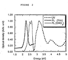
- BDT was found to fluoresce with an orange colour in the solid state and blue in dilute solution under UV irradiation.
- Figure 2 shows the UV absorption and emission spectra for the dimer.
- a ⁇ - ⁇ * gap of 2.8 eV in dilute solution (CHCl 3 as solvent) was observed from the absorption edge or from the photoluminescent emission peak, and 2.3 eV ⁇ - ⁇ * gap in solid film was obtained from its solid film'emission peak.
- the emissive properties of BDT may be exploited in organic electroluminescent devices.
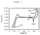
- Cyclic voltammetric measurement of the thin film of BDT revealed that both electrons and holes can be injected into the film, or in other words, BDT can be both n-doped or p-doped.
- Figure 3 shows a full sweep cyclic voltammogram for BDT film on Au coated glass substrate. A distinct colour change from yellow to brown to yellow was observed upon oxidative sweeping from 0 to 0.9 to 0 V (versus FOC), indicating an electrochemical quasi-reversible process upon p-doping (or hole injection) that may be related to the formation of a radical cation (see reference 17). A similar electrochemical process was noticed during the reduction sweep, suggesting a reversible n-doping (or election injection) process.
- BDT single crystal of BDT has been grown by the inventors by very slow cooling down of the saturated solution of BDT in toluene. Full crystallographic data were collected by a Synchrotron radiation source detailed below, as the single crystal was relatively small. Similar to ⁇ -6T and ⁇ -octathiophene, BDT crystallises in the monoclinic system, but has a C2/c space group. It is apparent that BDT has the greatest density, perhaps due to the high ratio of S/C in the molecule, or its highly packed structure. The BDT molecule has a completely planar conformation (see Figure 4), like 6 T and pentacene.
- each crystal unit cell there are four molecules packing in a unique way that differs from both 6T and pentacene.
- the BDT molecules packed more planar than either pentacene (which has a herringbone angle of 54°) or 6T (which has a herringbone angle of 66°) (see Figure 5).
- the BDT molecules in fact, pack each other face to face to form stacks with an angle of between two adjacent stacks.
- the driving force for this unique packing may be contributed from its advanced fused thiophene system and its sulphur atom's self-recognition.
- the BDT has the shortest ⁇ (A)- ⁇ (B) distance (3.56 ⁇ ) compared with 3.71 ⁇ for pentacene and 3.82 ⁇ for 6T, giving BDT a record close packing molecular system.
- the ⁇ (A)- ⁇ (B) stack distance is crucial to determine how strongly and how closely the parallel ⁇ systems will interact with each other; a shorter ⁇ stack distance should favour higher charge mobility.
- the shortest distance is between sulphur atoms of two tilted molecules, being 3.39 ⁇ .
- the invention exploits this phenomenon in processable organic thin films deposited by vapour and solution methods and is readily extended to include oligomers, polymers and precursor materials.
- TFTs Thin film transistors based on conjugated organic semiconductors are envisioned as the key component of low-cost, large-area electronics on flexible plastic substrates.
- the two most important material parameters for TFT applications are the field-effect mobility F FE and the ON/OFF ratio, i.e., the ratio of the current in the ON state of the TFT to that in the OFF state.
- F FE field-effect mobility
- ON/OFF ratio i.e., the ratio of the current in the ON state of the TFT to that in the OFF state.
- the film has to be highly crystalline with strong wavefunction overlap between adjacent molecules in the plane of the film.
- Intermolecular ordering is most easily achieved if a short-chain conjugated oligomer or a molecular semiconductor ( ⁇ -6T (reference 7), Cu-Pc (reference 19), C 60 (reference 20)) is deposited by vacuum sublimation.
- ⁇ -6T reference 7
- Cu-Pc reference 19
- C 60 reference 20
- fused ring compounds which have less conformational freedom than the prototype oligothiophenes (see reference 19) might yield stronger inter- and intramolecular ⁇ overlap. It is worth mentioning, however, that with conjugated polymers processed from solution a high degree of order can be obtained by making use of self-organisation mechanisms (see reference 20).
- TFTs comprising a fused ring compound of this invention, bis(dithienothiophene) (BDT) have exceptionally high ON/OFF ratios of up to 10 8 with sharp threshold characteristics.
- Field-effect mobilities are 0.0.2-0.05cm 2 /Vs.
- the TFT substrates were highly doped Si wafers with 2000 ⁇ SiO 2 gate oxide and interdigitated Au source/drain contacts.
- the surface of the SiO 2 was prepared so as to be hydrophobic by treating it with a solution of hexamethyldisilazane/chloroform (1:2) at 70 1 C for 3h. 100-200 nm thick BDT films were deposited by vacuum sublimation at a pressure of 1-2x10 -6 Torr.
- Optimum TFT performance was obtained for T ⁇ 100°C and r ⁇ 3 ⁇ /s.
- the TFT characteristics were measured with an HP 4145B parameter analyser under a dry N 2 atmosphere.
- FIG 6 shows the output (a) and transfer (b) characteristics of a typical BDT TFT deposited at 100°C.
- BDT is a p-type semiconductor and the devices operate in the accumulation mode.
- Typical ON/OFF ratios over a gate voltage range of 40V are 10 7 , but on some samples ON/OFF ratios up to 10 8 have been obtained (see Figure 6).
- the experimental characteristics are quadratic only in the range 5V ⁇
- ⁇ 20V and exhibits poor current saturation at higher gate voltages. Within the quadratic range, values of F sat FE 0.02-0.05 cm 2 /Vs are obtained under optimised deposition conditions (substrate temperature .1001C and deposition rates 1-3 ⁇ /s).
- These non-idealities may at least partly be related to a non-ohmic source/drain contact. As discussed below BDT is a high band gap semiconductor to which even a high workfunction metal like Au might not form an ohmic contact.
- the BDT material for the evaporation is purified by recrystallisation and vacuum thermal gradient sublimation. After the growth the films are transferred to a N 2 glove box within ⁇ 5 minutes, where the FET characteristics are measured. If stored under dry N 2 the TFT characteristics are stable over a period of weeks. However, operation in air results in rapid degradation. If the channel is turned on in air, I sd rapidly increases after a few minutes of operation and roughening around the Au hole-injecting source electrode is observed under an optical microscope, whereas the drain electrode remains intact. By Dektak profilometry the thickness of the Au source electrode is found to decrease in time (from initially 150nm to about 40nm after 2-3 hours of operation).
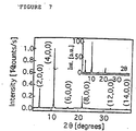
- Figure 7 shows a 6-2 ⁇ diffraction pattern of a 250nm BDT film deposited at ⁇ 100°C onto SiO 2 . In this geometry only Bragg reflections along the substrate normal can be measured. The observed pattern of sharp reflections can well be explained with the crystal structure of BDT, which has been determined by synchrotron XRD on a single crystal and has been described in detail above. It is sufficient to note that the unit cell is monoclinic with space group C2/c.
- the simulation shows that in the experimental diffraction pattern of the thin film only (h,0,0) reflections are observed (see inset of Figure 7). Their positions and intensities are in good agreement with the experimental pattern.
- Figure 8 shows polarised optical absorption spectra of a BDT film deposited' onto a Spectrosil glass substrate -held near 100°C.
- the absorption is characterised by two main peaks at 3.7eV and 4.7eV.
- the spectra exhibit a significant polarisation dependence confirming the high degree of structural order in the film.
- the absorption at 3.7eV is stronger by a factor of 2-3 for TM polarisation. Since the molecular axis is close to the substrate normal, this peak must correspond to transitions polarised along the long axis of the molecule.
- TM polarisation at least two weaker transitions around 2.65eV and 2.9eV below the main absorption at 3.7eV were reproducibly observed.
- the onset of absorption is at 2.4 ⁇ 0.2eV. It was determined by measuring a thick film (not shown) immersed into an inert liquid Teflon solution (Fluorinert FC-104, 3MTM) to reduce light scattering. The value is in good agreement with the photoluminescence spectra of BDT films exhibiting a peak at 2.25 eV.
- the relatively short conjugation length of the BDT molecule may explain the high ON/OFF ratio of the TFTs.
- Short chain molecules with a high ⁇ - ⁇ * energy gap tend to be more stable against unintentional chemical doping during synthesis and deposition.
- MIS metal-insulator-semiconductor
- the origin of the relatively high mobility must be related to the crystal structure of BDT.
- the long axis of the planar molecule is standing up on the substrate, which favours in-plane carrier transport along the stacking direction of the molecules.
- the coplanar stacking in BDT is likely to result in a stronger ⁇ - ⁇ overlap between adjacent molecules.
- the relatively high mobilities (0.02-0.05cm 2 /Vs) are explained by the coplanar stacking of the BDT molecules. Further improvement of the carrier mobility may be achieved by improving the carrier injection at the source/drain contacts and extending the' conjugation length using dithienothiophene as a building block.
- the largest peak and hole in the final difference map were 0.445 and -0.490 e ⁇ -3 .
- the lithiated dithienothiophene was added via syringe and refluxed for 1h. During this time the mixture turned dart red and some precipitation was observed.
- the mixture was cooled and poured into water (40 cm 3 ), the solids were filtered and washed with 2% aqueous HCl (2 x 50 cm 3 ), water (40 cm 3 ), aqueous Na 2 CO 3 then acetone (3 x 30 cm 3 ). Recrystallisation of the dark brown filter cake was attempted in toluene. This was difficult due to the intense dark brown coloration of the suspension in which dissolution was difficult to define. The mixture was allowed to cool slowly then the solids were filtered off to give a lighter brown filter cake.
- Carbon dioxide was added in small lumps to a flask against a fast flow of nitrogen. The flask was then sealed under a nitrogen bubbler and cooled to the -78°C. THF was added to cover the CO 2 and the mixture stirred. The cooled lithiodithienothiophene was added dropwise via syringe and a violent reaction was observed resulting in the formation of a yellow suspension. Once addition was complete the mixture was allowed to warm to r.t. during which time the mixture turned to an off white colour. After stirring for a further 30 min. water (30 cm 3 ) was added and the mixture turned to a light green/brown solution. This was washed with ether (2 x 20 cm 3 ) and the organics discarded.
- aqueous layer was acidified by the addition of HCl (10 cm 3 , 5 M) which precipitated out a fine yellow solid. Recrystallisation was attempted in 33% acetic acid. A fine, insoluble suspension remained after heating and this was left to further crystallise overnight to give the title compound as a fine yellow/green powder (286 mg, 61%); ⁇ H 7.31, (1H, d, J5.1), 7.56 (2H, d, J5.1), 7.94 (1H, s); ⁇ max/cm -1 (KBr) 3090 m, 2823 m, 2559 m, 1652 s, 1504 s, 1470 w, 1428 s, 1311 s, 1265 m, 1164 m, 928 s, 750 s, 716 s and 602 s; m.p. 276°C (sublimes) m.p.(lit.reference 29) 275-277°C)
- a solution of octanoyl chloride (1.00 g, 6.02 mmol) in dichloromethane (20 cm 3 ) was added dropwise over a 20 minute period and the mixture was then allowed to stand at room temperature for a further thirty minutes. It was then added to ice and the mixture was acidified with dilute hydrochloric acid (100 cm 3 ).
- Aluminium chloride (82 mg, 0.615 mmol) was dissolved in anhydrous diethyl ether (6. cm 3 ) and the solution was added slowly to an ice-cooled mixture of lithium aluminium hydride (103 mg, 2.71 mmol) in anhydrous diethyl ether (6 cm 3 ).
Landscapes
- Chemical & Material Sciences (AREA)
- Organic Chemistry (AREA)
- Engineering & Computer Science (AREA)
- Materials Engineering (AREA)
- Spectroscopy & Molecular Physics (AREA)
- Physics & Mathematics (AREA)
- Medicinal Chemistry (AREA)
- Polymers & Plastics (AREA)
- Chemical Kinetics & Catalysis (AREA)
- Health & Medical Sciences (AREA)
- Thin Film Transistor (AREA)
- Heterocyclic Carbon Compounds Containing A Hetero Ring Having Oxygen Or Sulfur (AREA)
- Polyoxymethylene Polymers And Polymers With Carbon-To-Carbon Bonds (AREA)
- Coupling Device And Connection With Printed Circuit (AREA)
- Electrotherapy Devices (AREA)
- Nitrogen Condensed Heterocyclic Rings (AREA)
- Organic Low-Molecular-Weight Compounds And Preparation Thereof (AREA)
Abstract
Description
- The present invention is concerned with conjugated organic compounds that can be used in electronic devices . In particular, fused thiophene oligomers or polymers can be used to fabricate thin-film transistors (TFTs) or field-effect transistors (FETs).
- Organic semiconductors that consist of conjugated oligomers or polymers are subject of considerable current research interest, due to their fundamental opto-electronic physics and their potential applications in photo-diodes (see reference 1), light-emitting devices (LEDs) (see reference 2) and thin film transistors (TFTs) (see reference 3) etc. The judicious choice of conjugated segments and their various combinations to form different length oligomers or polymers allows for sophisticated fine tuning of such molecular semiconductors, giving rise to surprisingly useful properties.
- Pioneered by Garnier and his co-workers, oligomers of thiophenes ranging from tetramers to octamers have been explored as active materials for TFTs that hold great promise in the fabrication of smart cards and flexible flat-panel displays (see references 4-6). The field effect charge mobility of thiophene oligomers was found to increase with conjugation length and then level off after the hexamer. Longer conjugation length seems to incur processing and purification problems as well as difficulty to achieve long range molecular ordering, and thus adversely affect field. effect mobility and on/off ratio.
- Soluble regioregular poly(3-hexylthiophene) has very recently shown high mobility (10-5 to 0.045 cm2/Vs) (see reference 7), although its on/off ratio was rather low (10 to 103) for reasons mentioned above. Therefore, the large majority of the past work into organic TFT materials has been concentrated on the hexamer of thiophene (or sexithiophene, a-hexathienyl, a-6T) and its alkylated derivatives. As a result, TFTs with mobilities of 0.03 cm2V-1s-1 and on/off ratios of more than 106 were achievable. The direction of high mobility in sexithiophene TFTs has been revealed to be parallel to the substrate and perpendicular to the long axis of the thiophene oligomer,' indicating the importance of π stacking to the contribution of charge mobility.
- Katz et al (see reference 8) have recently successfully explored another high mobility (0.04 cm2V-1s-1) organic TFT material, bis(benzodithiophene). The benzofused thiophenes may create greater overlap of the π-conjugated units though detailed crystalline structure was not given. Commercially available pentacene, a more advanced fused-ring compound, has received much less attention compared with thiophene oligomers in the past, probably because only low mobilities of 0.002 (see reference 9) or 0.009 cm2V-1s-1 (see references 10, 11) were achieved.
- Pentacene TFTs prepared by molecular beam deposition have recently shown high mobility (0.03 cm2V-1s-1). Using purer material and a slower deposition rate, workers raised pentacene TFTs to a record high mobility of 0.3-0.7 cm2V-1s-1 (see references 12, 13). The high mobility has been associated both with π stacking and the macroscopic single-crystal nature of sublimed pentacene films (see reference 14). Most organic materials suffer from poor "On/Off" characteristics (102-105) and high threshold slopes.
- An object of the present invention is to solve the above problems associated with prior art materials and devices. Accordingly, the present invention provides a compound or complex comprising at least two moieties, each moiety being comprised of two or more thiophenes fused directly to each other. In the context of this invention the term moiety is intended to extend to different parts of a single monomeric molecule and also repeating units of a dimer, oligomer or polymer.
- The present invention also provides a method for the production of a compound as defined above, which method comprises the coupling of one fused thiophene derivative to another fused thiophene derivative.
- The present invention further provides an electric, electronic, or optoelectronic component or device comprising a compound as defined above.
- The invention will now be described in further detail by way of example only, with reference to the accompanying drawings, in which:
- Figure 1 shows the configuration of top-contact TFTs (a) and bottom-contact TFTs (b);
- Figure 2 shows a UV absorption spectrum and emmision spectrum of BDT;
- Figure 3 shows a cyclic voltammogram of a BDT film on Au commencing from 0->0.9->0->-1.7->0 V (Et4BF4 in CH3CN, 0.1 M);
- Figure 4 shows the front and side view of a BDT molecule with numbering;
- Figure 5 shows packing views in a BDT crystal;
- Figure 6 shows output' (a) and transfer characteristics (b) of a BDT TFT deposited at 100°C (channel length L=20 Fm, channel width W=1 cm, BDT thickness=200 nm);
- Figure 7 shows the 0-2 diffraction pattern of a 250nm BDT film on SiO2 deposited at .100°C measured with Cu Kα radiation - the inset shows a theoretical simulation of the pattern using the Cerius2 Molecular Simulations program - it assumes the single crystal structure of BDT and a preferential orientation of the grains with the bc plane of the unit cell in the substrate plane;
- Figure 8 shows the polarised optical absorption (circles) at an angle of incidence of 60° (see inset) of a 300Å BDT film deposited at 100°C on a glass substrate - the spectrum drawn as a solid line shows the enlarged TM spectrum near the onset of absorption; and
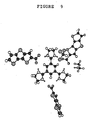
- Figure 9 shows the x-ray structure of the complex 12.
-
- The present invention uses organic semiconductors based on fused thiophenes in which the use of a thin layer of the material enables the fabrication of solid state heterostructural devices for instance, thin-film transistors (TFTs) with high performance. The organic semiconductors consist of oligomers or polymers based on fused thiophenes, which allow a maximal intermolecular π overlapping to form compressed π stacks in a supramolecular structure. High field-effect mobility and high On/Off ratio can therefore be achieved using this sort of organic semiconductor as an active material.
- The present invention provides a means to design and synthesise organic semiconductors with both high mobilities and On/Off ratios used for use in high performance TFTs or FETs. The fused thiophenes, typically dithieno[3,2-b:2',3'-d]thiophene are employed as building blocks for oligomers or polytriers. The fused thiophenes not only provide a planar conjugated segment but also a sulphur rich source, which may adjust molecular structure and ordering. High field effect mobilities of 0.05 cm2V-1s-1 and high On/Off ratios of more than 108 have been achieved. Specifically X-ray analysis of a single crystal of α,α'-bis(dithieno[3,2-b:2',3'-d]thiophene) shows for the first time a face to face π stacking with the shortest interplanar distance of 3.56 Å. In this regard, even high mobility could be achieved if a macroscopic single crystal of this material could be realised during device fabrication.
- This invention refers to the synthesis of novel fused heterocyclic ring compounds, their oligomers and polymers and their application as active materials in electronic devices, specifically thin film transistors. The fused heterocycles (more specifically thiophenes) may consist of two, three, four and five-fused thiophenes, preferably the three fused thiophenes (Scheme 1). Specifically the fused thiophene "dimer" 5 exemplifies the invention. In order to render the conjugated oligomers or polymers into solution processable 'form solubilising side chains may be attached or deposition of films may take place from solution using precursor materials.
- Solubilising groups can have an advantageous effect on solution processability and supramolecular order in the active layer of a device. They may be attached at various positions on the heterocyclic ring to afford solution-processable organic materials. Solution processability plays an important part in controlling the morphology of the final thin film. Oligometric and polymeric substances may be selected from one of the following categories (Scheme 1). Monomeric units may also be selected from the representative examples shown in Scheme 1:

- In Scheme 1, R1, R2, R3 and R4 may be selected from any combination of the following H, (CH2)nCH3, O(CH2)nCH3, S(CH2)nCH3, or a branched chain derivative carrying aryl, alkyl or heterocyclic substituents or other solubilising side chain alkyl, aryl or heterocyclic substituents. R1 may also be COOH, triazole, tetrazole or a derivative thereof.
- Preferred oligomers include 4 (R1=C8H17, R2=R3=R4=H); 5 (R1=C6H13S-, R2=R3=H); 5 (R1=C8H17, R2=R3=H); 5 (R1=C10H21S-, R2=R3=H); 5 (R1=C12H25, R2=R3=H); 5 (R1=C12H25S-, R2=R3=H); 2 (R1=COOH, R2=R3=R4=H) ; and 2 (R1=COOH, R2=R3=H, R4= C8H17).
- Polymeric units may be selected from the structure 6 and a selection of repeat units from scheme 2:

- In scheme 2, R1, R2, and R3 may be selected from any combination of the following H, (CH2)nCH3, O(CH2)nCH3, S(CH2)nCH3, or a branched chain derivative carrying aryl, alkyl or heterocyclic substituents or other solubilising side chain alkyl, aryl or heterocyclic substituents. R1 may also be COOH, triazole, tetrazole or a derivative thereof.
- Preferably, polymers 6 will carry the repeat unit 10 (R1=H, R2=alkyl, R3=H) and 10 (R1=R2=alkyl, R3=H).
- Recent work by Kraft et al (see reference 27) has shown that self assembled dendrimers provided by hydrogen bonding between aryl carboxylic acids and poly-imidazole bases can form large planar complexes. The complex 12 of the carboxylic acid 2 (R1=COOH, R2=R3=R4=H) shown in scheme 3 with tris(4,5-dihydroimidazol-2-yl)benzene gave the complex shown in scheme 3 (see also Figure 9). This surprisingly shows considerable. order, as evidenced by Synchrotron X-ray analysis. Such order may lend itself to the formation of highly ordered films for FETs, and furthermore the supramolecular ordering may be manifested in high mobility transistor materials.

- Further supramolecular assembled complexes analogous to the complex 12 of scheme 3 based on 2 (R1=C8H17 or C6H13S-, R2=R3=H, R4=COOH) have been made. A specific embodiment is the complex 13 derived from 2 (R1=C8H17, R2=R3=H, R4=COOH) and 1,3,5-tris(dihydroimidazole). This shows interesting mesophase behaviour, which will contribute to the control of supramolecular order. In the present invention exploitation of supramolecular order allows special processing and orientation of materials to achieve high mobilities in FETs.
- In a particular embodiment α,α'-bis(dithieno[3,2-b:2',3'-d]thiophene) (BDT) (5 (R1=R2=R3=H)), the "dimer" of 2 (R1=R2=R3=R4=H), has been synthesised and fully characterised. The fused thiophene compound, dithieno[3,2-b:2',3'-d]thiophene (2 (R1=R2=R3=R4=H)) was synthesised according to a published protocol, starting from 3-bromothiophene (see reference 15). The "dimerisation" was carried out through the coupling reaction of a-lithiated monomer 3 using ferric acetylacetonate as an oxidative coupling reagent (Scheme 4). Other coupling reagents, e.g. CuCl2, also caused' coupling. BDT (5 (R1=R2=R3=H)) was just soluble enough in boiling toluene or hot DMF for recrystallisation, and slightly soluble in THF (2 g/l), allowing for great convenience in purification and identification by 1H NMR. Its microcrystal powder has a gold like lustre and shows no chemical change in ambient conditions within a test time of 2 months. Various characterisations, 1H NMR, UV, FTIR, microanalysis and high resolution mass spectroscopy, are all in agreement with the structure of 5 (R1=R2=R3=H).For further purification, the dimer BDT was readily sublimed at 2001C under vacuum (10-4-10-5 mmHg) in a gradient sublimation tube (see reference 16). The resulting sample of BDT has a finer crystalline size and lighter colour than before sublimation.

- BDT was found to fluoresce with an orange colour in the solid state and blue in dilute solution under UV irradiation. Figure 2 shows the UV absorption and emission spectra for the dimer. A π-π* gap of 2.8 eV in dilute solution (CHCl3 as solvent) was observed from the absorption edge or from the photoluminescent emission peak, and 2.3 eV π-π* gap in solid film was obtained from its solid film'emission peak. The emissive properties of BDT may be exploited in organic electroluminescent devices.
- Cyclic voltammetric measurement of the thin film of BDT revealed that both electrons and holes can be injected into the film, or in other words, BDT can be both n-doped or p-doped. Figure 3 shows a full sweep cyclic voltammogram for BDT film on Au coated glass substrate. A distinct colour change from yellow to brown to yellow was observed upon oxidative sweeping from 0 to 0.9 to 0 V (versus FOC), indicating an electrochemical quasi-reversible process upon p-doping (or hole injection) that may be related to the formation of a radical cation (see reference 17). A similar electrochemical process was noticed during the reduction sweep, suggesting a reversible n-doping (or election injection) process. No apparent colour change was observed during the reduction sweep. According to its redox peak positions, the HOMO/LUMO level of -5.6 eV/-3.3 eV was estimated for BDT, indicating a band gap of 2.3 eV from electrochemical measurement that is in good agreement with its solid state band gap measured from its electronic spectroscopic measurements. When the oxidation potential was larger than 1.2V, a two-electron injection feature was observed, and the BDT colour changed to dark green or black, indicating perhaps the formation of a di-cation which is quite universal for conjugated polymers (see references 17,18).
- A single crystal of BDT has been grown by the inventors by very slow cooling down of the saturated solution of BDT in toluene. Full crystallographic data were collected by a Synchrotron radiation source detailed below, as the single crystal was relatively small. Similar to α-6T and α-octathiophene, BDT crystallises in the monoclinic system, but has a C2/c space group. It is apparent that BDT has the greatest density, perhaps due to the high ratio of S/C in the molecule, or its highly packed structure. The BDT molecule has a completely planar conformation (see Figure 4), like 6 T and pentacene.
Crystallographic data of BDT (collected at 160±2 K) Chemical formula C16H6S6 Formular weight 390.57 Wavelength 0.68790Å Crystal system Monoclinic Space group C2/c Unit cell dimensions a=33.689(2)Å, α= 90° b=3.8834(2)Å, β=101.0932(2)° c=11.1055(5)Å, γ=90° Volume . 1425.75(13) Å3 z 4 Density (calculated) 1.820 Mg/m3 Absorption coefficient 0.948 mm-1 F(000) 792 Crystal size 0.07x0.02x0.02 mm Q range for data collection 3.58 to 26.89° Index ranges -42< h <34, -4< k <5, -14< l < 13 Reflections collected 1272 Independent reflections 813 (Rint = 0.0429) Absorption correction Sadabs Refinement method Full-matrix least-squares on F2 Data/restraints/parameters 813/0/100 Goodness-of-fit on F2 1.043 Final R indices [I>2 s(I)] R1=0.078, wR2=0.1265 R indices (all data) R1=0.0556, wR2=0.1314 Large diff. peak and hole 0.44 and -0.490 eÅ-3 Bond lengths[Å] and angles [°] for BDT S(1)-C(4) 1.738(4) S(1)-C-(S) 1.739(4) S(2)-C(1) 1.724(4) S(2)-C(2) 1.726(4) C(9)-C(7) 1.377(6) C(9)-C(5) 1.410(5) C(9)-H.(9) 0.95 C(6)-C(1) 1.356(6) C(6)-C(4) 1.428(6) C(6)-H(6) 0.95 C(5)-C(3) 1.392(6) C(4)-C(2) 1.378(6) C(3)-C(2) 1.426(5) C(3)-S(3) 1.724(4) C(1)-H(1) 0.95 S(3)-C(7) 1.750(4) C(7)-C(7)* 1.445(7) C(4)-S(1)-C(5) 90.0(2) C(1)-S(2)-C(2) 90.7(2) C(7)-C(9)-C(5) 112.0(3) C(7)-C(9)-H(9) 124.0(2) C(5)-C(9)-H(9) 124.0(2) C(1)-C(6)-C(4) 110.3(4) C(1)-C(6)-H(6) 124.9(2) C(4)-C(6)-H(6) 124.9(2) C(3)-C(5)-C(9) 113.7(4) C(30)-C(5)-S(1) 112.9(3) C(9)-C(5)-S(1) 133.4(3) C(2)-C(4)-C(6) 113.8(4) C(2)-C(4)-S(1) 113.3(3) C(6)-C(4)-S(1) 132.9(3) C(5-)-C(3)-C(2) 111.7(3) C(5)-C(3)-S(3) 111.1(3) C(2)-C(3)-S(3) 137.2(3) C(4)-C(2)-C(3) 112.0(4) C(4)-C(2)-S(2) 111.1(3) C(3)-C(2)-S(2) 136.9(3) C(6)-C(1)-S(2) 114.2(3) C(6)-C(1)-H(1) 122.9(2) S(2)-C(1)-H(1) 122.9(2) C(3)-S(3)-C(7) 91.4(2) C(9)-C(7)-C(7) 128.4(5) C(9)-C(7)-S(3) 111.9(3) C(7)*-C(7)-S(3) 119.7(4) - In each crystal unit cell, there are four molecules packing in a unique way that differs from both 6T and pentacene. Surprisingly, instead of herringbone packing, the BDT molecules packed more planar than either pentacene (which has a herringbone angle of 54°) or 6T (which has a herringbone angle of 66°) (see Figure 5). The BDT molecules, in fact, pack each other face to face to form stacks with an angle of between two adjacent stacks. The driving force for this unique packing may be contributed from its advanced fused thiophene system and its sulphur atom's self-recognition.
- Comparing the minimum distance between two molecules for the three materials, it is noted that the BDT has the shortest π(A)-π(B) distance (3.56 Å) compared with 3.71 Å for pentacene and 3.82 Å for 6T, giving BDT a record close packing molecular system. The π(A)-π(B) stack distance is crucial to determine how strongly and how closely the parallel π systems will interact with each other; a shorter π stack distance should favour higher charge mobility. In the BDT system, the shortest distance is between sulphur atoms of two tilted molecules, being 3.39 Å. The invention exploits this phenomenon in processable organic thin films deposited by vapour and solution methods and is readily extended to include oligomers, polymers and precursor materials.
- Thin film transistors (TFTs) based on conjugated organic semiconductors are envisioned as the key component of low-cost, large-area electronics on flexible plastic substrates. The two most important material parameters for TFT applications are the field-effect mobility FFE and the ON/OFF ratio, i.e., the ratio of the current in the ON state of the TFT to that in the OFF state. To obtain high carrier mobilities at the interface between the thin organic film and the gate dielectric, the film has to be highly crystalline with strong wavefunction overlap between adjacent molecules in the plane of the film. Intermolecular ordering is most easily achieved if a short-chain conjugated oligomer or a molecular semiconductor (α-6T (reference 7), Cu-Pc (reference 19), C60 (reference 20)) is deposited by vacuum sublimation. The inventors considered that fused ring compounds, which have less conformational freedom than the prototype oligothiophenes (see reference 19) might yield stronger inter- and intramolecular π overlap. It is worth mentioning, however, that with conjugated polymers processed from solution a high degree of order can be obtained by making use of self-organisation mechanisms (see reference 20).
- For many memory and display applications a high ON/OFF ratio exceeding 10 is an even more important requirement than a high mobility. It requires a low extrinsic doping level. Most organic TFTs yield relatively low ON/OFF ratios of 103-106 (see references 8, 20, 21). An ON/OFF ratio of 108 has been claimed for pentacene TFTs, which require, however, a voltage range of 200V, too large to switch between ON and OFF states (see reference 12). So far, the sharpest turn-on characteristics with ON/OFF ratios of 106-107 have been reported for carefully purified α-6T (see reference 22).
- TFTs comprising a fused ring compound of this invention, bis(dithienothiophene) (BDT) have exceptionally high ON/OFF ratios of up to 108 with sharp threshold characteristics. Field-effect mobilities are 0.0.2-0.05cm2/Vs. The TFT substrates were highly doped Si wafers with 2000Å SiO2 gate oxide and interdigitated Au source/drain contacts. The surface of the SiO2 was prepared so as to be hydrophobic by treating it with a solution of hexamethyldisilazane/chloroform (1:2) at 701C for 3h. 100-200 nm thick BDT films were deposited by vacuum sublimation at a pressure of 1-2x10⁻⁶ Torr. The substrate temperature and evaporation rate were varied between room temperature and ≈130°C and r=0.2-10Å/s, respectively. Optimum TFT performance was obtained for T≈100°C and r≈3Å/s. The TFT characteristics were measured with an HP 4145B parameter analyser under a dry N2 atmosphere.
- Figure 6 shows the output (a) and transfer (b) characteristics of a typical BDT TFT deposited at 100°C. As with most other conjugated organic materials, BDT is a p-type semiconductor and the devices operate in the accumulation mode. A small reverse gate bias of 2-6V is sufficient to turn the channel off (IOFF=2-3pA), which implies that the material is only slightly p-doped. Typical ON/OFF ratios over a gate voltage range of 40V are 107, but on some samples ON/OFF ratios up to 108 have been obtained (see Figure 6). The turn-on characteristics are sharp, with a small subthreshold slope S=(d(logIsd)/dVg)-1 of 0.6V/decade. These are believed to be the best ON/OFF characteristics reported for an organic TFT. They are comparable to those of an a-Si TFT (see reference 23).
- Charge carrier mobilities, however, are still an order of magnitude lower than for α-Si. From the transfer characteristics in the saturation regime the mobility is extracted according to the following equation (see reference 24) :
- The TFT characteristics in Figure 6 reveal some non-idealities. Near Vds=0, the output characteristics are nonlinear, especially for higher gate voltages. Above Vg.20V current saturation becomes poor and Vsd has to significantly exceed |Vg-VT| to drive the transistor into saturation. These non-idealities may at least partly be related to a non-ohmic source/drain contact. As discussed below BDT is a high band gap semiconductor to which even a high workfunction metal like Au might not form an ohmic contact.
- To obtain ON/OFF ratios of 108 the BDT material for the evaporation is purified by recrystallisation and vacuum thermal gradient sublimation. After the growth the films are transferred to a N2 glove box within ≈5 minutes, where the FET characteristics are measured. If stored under dry N2 the TFT characteristics are stable over a period of weeks. However, operation in air results in rapid degradation. If the channel is turned on in air, Isd rapidly increases after a few minutes of operation and roughening around the Au hole-injecting source electrode is observed under an optical microscope, whereas the drain electrode remains intact. By Dektak profilometry the thickness of the Au source electrode is found to decrease in time (from initially 150nm to about 40nm after 2-3 hours of operation). The Dektak results unambiguously indicate that in spite of the high reduction potential and inertness of Au, an electrochemical reaction and/or electromigration occurs at the contact between BDT and' the hole-injecting Au electrode. The reaction only occurs in the presence of water and/or O2 and may also be related to the presence of sulphur in BDT. This contact instability, which may be solved by a different source/drain metallisation or by encapsulation, has so far prevented study of the stability of BDT itself against doping in air.
- Since the molecular order of the film is crucial for the carrier transport in the TFT the structure of the polycrystalline BDT films has been investigated by X-ray diffraction (XRD). Figure 7 shows a 6-2 diffraction pattern of a 250nm BDT film deposited at ≈100°C onto SiO2. In this geometry only Bragg reflections along the substrate normal can be measured. The observed pattern of sharp reflections can well be explained with the crystal structure of BDT, which has been determined by synchrotron XRD on a single crystal and has been described in detail above. It is sufficient to note that the unit cell is monoclinic with space group C2/c. The cell parameters are a=33.689Å, α=90°, b=3.883Å, β=101.093°, c=11.106 Å, γ=90°. Using the single crystal structure the powder diffraction pattern of BDT has been simulated. The simulation shows that in the experimental diffraction pattern of the thin film only (h,0,0) reflections are observed (see inset of Figure 7). Their positions and intensities are in good agreement with the experimental pattern. These results prove that all grains of the polycrystalline film are oriented with the be plane of the unit cell parallel to the substrate. In this orientation the long axis of the molecule is close to the substrate normal.
- Figure 8 shows polarised optical absorption spectra of a BDT film deposited' onto a Spectrosil glass substrate -held near 100°C. The absorption is characterised by two main peaks at 3.7eV and 4.7eV. The spectra exhibit a significant polarisation dependence confirming the high degree of structural order in the film. The absorption at 3.7eV is stronger by a factor of 2-3 for TM polarisation. Since the molecular axis is close to the substrate normal, this peak must correspond to transitions polarised along the long axis of the molecule. For TM polarisation at least two weaker transitions around 2.65eV and 2.9eV below the main absorption at 3.7eV were reproducibly observed. The onset of absorption is at 2.4±0.2eV. It was determined by measuring a thick film (not shown) immersed into an inert liquid Teflon solution (Fluorinert FC-104, 3M™) to reduce light scattering. The value is in good agreement with the photoluminescence spectra of BDT films exhibiting a peak at 2.25 eV.
- The BDT spectra bear a striking similarity to the polarised absorption spectra of oligothiophenes n-T (n=4,5,6,8) (see reference 25), for which it has been shown that the energy of the strong π-π* peak along the molecular axis shifts to lower energy with increasing conjugation length of the molecule (4T: Emax=3.8eV; 5T: 3.55eV; 6T: 3.0eV). In BDT the transition occurs at 3.7eV which suggests that the conjugation length of the BDT molecule is relatively short, similar to 4T. This is reasonable as Hückel molecular orbital (MO) calculations indicate that in the highest occupied MO (HOMO) and the lowest unoccupied MO (LUMO) there is only small charge density on the centre sulphur atom in each of the two fused ring units making BDT look similar to 4T.
- The relatively short conjugation length of the BDT molecule may explain the high ON/OFF ratio of the TFTs. Short chain molecules with a high π-π* energy gap tend to be more stable against unintentional chemical doping during synthesis and deposition. From capacitance-voltage measurements on metal-insulator-semiconductor (MIS) diodes the extrinsic doping level of BDT is estimated to be on the order of 1-2x1016 cm-3. This small value is in good agreement with the magnitude of the reverse gate voltage (2-6V) required to turn the channel off, i.e., deplete the 200nm thick BDT film.' However, it is surprising that such a short chain molecule yields relatively high mobilities of 0.02-0.05cm2/Vs, higher than mobilities measured in α-6T (0.01-0.03cm2/Vs) (see reference 1) and 4T (2-5x10⁻³cm2/Vs) (see reference 25).
- The origin of the relatively high mobility must be related to the crystal structure of BDT. As in the oligothiophenes, the long axis of the planar molecule is standing up on the substrate, which favours in-plane carrier transport along the stacking direction of the molecules. However, there is an important difference between the packing of the molecules in BDT and in the oligothiophenes. According to the single. crystal XRD results (see above) the packing of nearest-neighbour, face-to-face molecules in BDT is not of the herringbone type. The molecular planes along the π-π stacking direction are strictly parallel to each other whereas in all oligothiophenes they enclose the herringbone angle (τ=66° for α-6T) (see reference 26). The coplanar stacking in BDT is likely to result in a stronger π-π overlap between adjacent molecules. The smallest S-S and C-C distances between face-to-face molecules are b=3.39Å and 3.56 Å, compared to 4.19 Å and 3.56 Å in α-6T. This important difference in the crystal structure may explain the relatively high carrier mobilties in spite of the small conjugation length.
- BDT is an excellent material for organic TFTs. It yields exceptionally high ON/OFF ratios up to 108 and sharp turn-on characteristics with subthreshold slope of S=0.6V/decade, comparable to α-Si TFTs. The relatively high mobilities (0.02-0.05cm2/Vs) are explained by the coplanar stacking of the BDT molecules. Further improvement of the carrier mobility may be achieved by improving the carrier injection at the source/drain contacts and extending the' conjugation length using dithienothiophene as a building block.
- Dithieno[3,2-b:2',3'-d]thiophene (2 (R1=R2=R3=R4=H)) was synthesised according to a published method starting with 3-bromothiophene (see reference 15).
m.p. 66-68°C
1H NMR (CD2Cl2, 250MHz) : δ 7.33 (2 H, d, J 5.2), 7.41 (2 H, d, J 5.2).
13C NMR (CD2Cl2, 100 MHz) : δ 121.0, 126.2, 131.0, 141.9. - Bis(dithieno[3,2-b:2',3'-d]thiophene) (5 (R1=R2=R3=H)) : Butyl lithium (1.6 M, 1.17 mmol) was added into a solution of 2 (R1=R2=R3=H) (230 mg, 1.17 mmol) in dry THF (5 ml) at -78°C slowly. After being stirred for one hour, an organolithium solution was added via a cannular tube into a refluxing solution of ferric acetylacetonate [Fe(acac)3) (413 mg, 1.17 mmol) in THF (5 ml). The dark red mixture was refluxed under argon for 2 hours, and then poured into water (100 ml) to give a brown solid. After filtration, the solid was washed with dilute HCl (2 %), water, dilute Na2CO3 (10 %) and acetone respectively. The final light brown powder was recrystallised from toluene twice to give gold like flake crystals (130 mg, 57 %).
m.p. 3171C (DSC, 10°C /min, N2);
1H NMR (THF-d8, 250 MHz): δ 6.95 (2H, d, J 5.2), 7.51 (2H, d, J 5.2 ), 7.85 (2H, s);
FTIR (KBr) νmax/cm-1 3070 s, 1670 m, 1465 m, 1427 m, 1364 s, 1185 m, 1072 m, 897 m, 796s, 688 s, 593 s;
UV λmax: 392 nm;
Found: C, 49.2%; H, 1.51%; HRMS: 389.8794(M+),
C16H6S6 requires C, 49.2%; H, 1.55%; M+ 389.8794. - Data were collected at the Daresbury Synchrotron radiation source, station 9.8, using a Siemens SMART COD diffractometer (courtesy of Dr N. Feeder and Dr W Clegg). A frame width of 0.30 was used, with a 2s exposure per frame. All data were collected at 160K. Of a total of 1272 collected reflections, 813 were independent [R(int) = 0.0429; (3.58≤q≤26.89)].
- The structure was solved by direct methods (S1R92) and refined by full-matrix least-squares on F2 (SHELXL93) to final values of R1 [I>2s(I)]=0.047 and wR2=0.1265, S=1.112 {w=1/[\s2(Fo2)+(0.0977P)2], where P=(Fo2+2Fc2)/3}.
- The largest peak and hole in the final difference map were 0.445 and -0.490 eÅ-3.
-

- The method Ng was followed (see reference 28). Dithienothiophene 2 (R1=R2=R3=R4=H) (1.178 g, 6.0 mmol) was dissolved in dry THF (5 cm3) and stirred under argon at -78°C, n-Butyl lithium (4 cm3, 1.5 M, 6.0 mmol) was added dropwise with stirring. During this addition a yellow suspension formed and the mixture was allowed to warm to r.t. After stirring at r.t for a further 45 min. the mixture was cooled to 0°C and dihexyl disulfide (1.41 cm3, d 0.95, 6.0 mmol) was added dropwise. The mixture was stirred at r.t. for 1 h. then refluxed for 45 min. before being cooled and poured into water (20 cm3). The products were extracted with ether (3 x 50 cm3), washed with sodium hydroxide solution (50 cm3, 2%) then water before drying (Na2SO4) and evaporation to give a dark green oil. This was purified by vacuum packed column chromatography (20 x 4.5 cm silica with hexane) to give the title compound 2 (R1=C6H13S-, R2=R3=R4=H) ( 1 . 2 02 g, 64%); Rf(hexane) 0.28; δH 0.89 (3H,t, J6.9), 1.23-1.48 (6H,m), 1. 66 (2H, pentet, J7.3), 2.85 (2H, t, J7.3), 7.27 (1H, d, J5.3), 7.33 (1H, s), 7.35 (1H, d, J5.3); δc 14.0 (CH3), 22.6 (alkyl), 28.1 (alkyl), 29.5 (alkyl), 31.4 (alkyl), 39.4 (S-CH2), 120.7 (ArCH), 126.2 (ArCH), 131.0 (ArCH), 133.4 (Ar q), 135.8 (Ar q), 140.3 (Ar q) and 141.4 Ar q); m/z 314 (M++2, 15%), 313 (M+=1, 11), 312 (M+, 65), 230 (18), 229 (20), 228 (100), 227 (66) , 196 (22), 183 (34), 152(24), 151 (18), 69 (19), 43 (53) and 41 (56); m/z calc 12C14 1H16 32S4 312.001348, found 312.013500; u max/cm-1 (CDCl3) 3090 w, 2958 s, 2930 s, 2858 m, 2359 w, 2246 w, 1466 m, 1360 s, 1189 w, 1153 w, 1088 m, 1001 w, 964 w, 829 m and 604 m.
- 2-(1-thiohexyl-dithienothiophene 2(R1=C6H13S, R2=R3=R4=H) (200 mg, 0.64 mmol) was dissolved in dry THF (4 cm3) and stirred under nitrogen at 0°C, n-Butyl lithium (0.40 cm3, 1.6 M, 0.64. mmol) was added dropwise with stirring. During this addition the mixture turned green and retained this colour on stirring at r.t for 40 min. Ferric acetylacetonate (226 mg, 0.64 mmol) was suspended in dry THF (4 cm3) and refluxed under nitrogen. The lithiated dithienothiophene was added via syringe and refluxed for 1h. During this time the mixture turned dart red and some precipitation was observed. The mixture was cooled and poured into water (40 cm3), the solids were filtered and washed with 2% aqueous HCl (2 x 50 cm3), water (40 cm3), aqueous Na2CO3 then acetone (3 x 30 cm3). Recrystallisation of the dark brown filter cake was attempted in toluene. This was difficult due to the intense dark brown coloration of the suspension in which dissolution was difficult to define. The mixture was allowed to cool slowly then the solids were filtered off to give a lighter brown filter cake. This was dissolved in THF and residual solids (presumably Fe(acac)2) were filtered off. The THF was evaporated off and a further. recrystallisation from toluene gave a gold solid (68 mg, 34%) which was found to be the title compound; δH (400 MHz, THF-d8) 0.91 (3H, t, J7.0), 1.30-1.38 (6H, m), 1.47 (2H, pentet, J7.3), 2.92 (2H, t, J7.4), 7.44 (1H, s), 7.60 (1H, s) ; m/z 624 (M++2, 1%), 622 (M+, 2) , 537 (1) , 506 (2) , 421 (4), 277 (7), 199 (10), 149 (15), 135 (15), 121 (17), 91 (62), 81 (65), 69 (100) and 55 (40); m/z calc. 12C28 1H30 32S8 622.011318, found 622.011300; nmax /cm-1 (KBr) 2954 m, 2924 s, 2854 m, 1466 m, 1426 m, 1361 s, 1161 w, 1001 w, 924 m, 788 s, 688 m, and 594 m; C28H30S8 requires C, 53.98; H, 4.85; Found C, 52.68; H, 4.25; Fe, 0.23. The compound was found to sublime at 1.5 x 10⁻⁵ Torr/175°C. Approximate field effect mobility was 10-3 cm2V-1S- 1; Approximate On/Off ratio 106.
- The method of Gronowitz et al (see reference 28) was followed. Dithienothiophene 2 (R1=R2=R3=R4=H) (368 mg, 1.88 mmol) was dried by heating under vacuum in a Schlenk tube. After purging with nitrogen, dry THF (4 cm3) was added and the resulting solution stirred at -78°C. n/Butyl lithium (1.175 cm3, 1.60 M, 1.88 mmol) was added dropwise to the cold stirred solution which turned cloudy green after stirring for 10 min., but gave a transparent green solution on warming to r.t.. The solution was stirred at r.t. for a further 40 min. then cooled to around -40°C (not so cold as to precipitate out the lithiodithienothiophene).
- Carbon dioxide was added in small lumps to a flask against a fast flow of nitrogen. The flask was then sealed under a nitrogen bubbler and cooled to the -78°C. THF was added to cover the CO2 and the mixture stirred. The cooled lithiodithienothiophene was added dropwise via syringe and a violent reaction was observed resulting in the formation of a yellow suspension. Once addition was complete the mixture was allowed to warm to r.t. during which time the mixture turned to an off white colour. After stirring for a further 30 min. water (30 cm3) was added and the mixture turned to a light green/brown solution. This was washed with ether (2 x 20 cm3) and the organics discarded. The aqueous layer was acidified by the addition of HCl (10 cm3, 5 M) which precipitated out a fine yellow solid. Recrystallisation was attempted in 33% acetic acid. A fine, insoluble suspension remained after heating and this was left to further crystallise overnight to give the title compound as a fine yellow/green powder (286 mg, 61%); δH 7.31, (1H, d, J5.1), 7.56 (2H, d, J5.1), 7.94 (1H, s); ν max/cm-1 (KBr) 3090 m, 2823 m, 2559 m, 1652 s, 1504 s, 1470 w, 1428 s, 1311 s, 1265 m, 1164 m, 928 s, 750 s, 716 s and 602 s; m.p. 276°C (sublimes) m.p.(lit.reference 29) 275-277°C)
- Dithienothiophene-2-carboxylic acid 2 (R1=COOH, R2=R3=R4=H) (240 mg, 1 mmol) and tris(4,5-dihydroimidazol-2-yl)benzene (93 mg, 0.33 mmol) were dissolved by refluxing in a mixture of 20 cm3 EtOH and 150 cm3 of CHCl3. This gave a turbid solution which was filtered whilst hot through a fine sinter and allowed to cool and stand overnight. Very little precipitation was observed and so the volume of the mixture was evaporated down. to 40 cm3 and cooled in the freezer. Again very little precipitation was observed and so the solvents were evaporated down to 20 cm3 at which point the products rapidly precipitated from solution and would not re-dissolve until the original quantities of solvents were added and the mixture refluxed. The mixture was evaporated to dryness then redissolved in the ethanol and chloroform in the same fashion as before. On this occasion, very careful evaporation at 50°C close to atmospheric pressure gave rise to a small quantity of precipitate once the solvent volume was reduced to about 30 cm3. On cooling the solution and then leaving it to stand in the freezer overnight a large quantity of the complex 12 had precipitated had developed. This was filtered off to give 189.1 mg, 57%, m.p. 265°C (decomp.); δH (CD3OD, 500 MHz) 7.38 (3H, d, J5.1), 7.59 (3H, d, J5.1), 7.84 (3H, s) and 8.48 (3H, s). νmax/cm-1 (KBr) 3086, 2924, 2706, 1582.
- 2'-Octyldithienothiophene-2-carboxylic acid (130 mg, 0.369 mmol) and 1,3,5-tris(4,5-dihydroimidazol-2-yl)benzene (34.7 mg, 0123 mmol) were dissolved in hot ethanol (30 ml)/dichloromethane (20 ml). The yellow solution was filtered whilst hot, concentrated in vacuum to about 35 ml until a solid started to precipitate from solution, once more heated to reflux and left to stand at -20°C for 2 d. The yellow precipitate was collected by suction filtration, washed with ethanol (10 ml) and dried at 60°C/10-6 mbar. Yield of 13 42 mg (25%). As suspected, the octyl substituent depresses the melting point of the compound to about 160-165°C. Upon melting, a mesophase with relatively low viscosity can be detected 1H NMR (500 MHz, CDCl3, 1.1 mg/0.8 ml) : δ=0.88 (t, J=7. 0 Hz, CH3), 1.23-1.43 (m), 1.73 (qui., J=7.4 Hz, CH2), 2.90 (t, J=7.4 Hz, CH2), 4.22 (s, NCH2), 6.98 and 7.80 (s, thiophene-CH), 10.00 (s; C6H3), 12.8 (br. s, NH) ; IR (KBr) :νmax/cm-1 3426 (m), 2925 (m), 1582 (s) , 1500 (m), 1372 (s), 1288 (m), 773 (m), 694 (m); C66H78N6O6S9 (1339.92): Calc. C 59.16, H 5.87, N 6.27; Found C 58.89, H5.82, N 6.37; Octanoyl-dithienothiophene 2 (R1=COC7H15, R2=R3=R4=H)

- Dithienothiophene 2 (R1=R2=R3=R4=H) (765 mg, 3.90 mmol) was dissolved in dry dichloromethane (35 cm3) and the solution was ice-cooled before AlCl3 (790 mg, 5.92 mmol) was added in one portion yielding a dark mixture. A solution of octanoyl chloride (1.00 g, 6.02 mmol) in dichloromethane (20 cm3) was added dropwise over a 20 minute period and the mixture was then allowed to stand at room temperature for a further thirty minutes. It was then added to ice and the mixture was acidified with dilute hydrochloric acid (100 cm3). Additional dichloromethane (100 cm3) was added and the layers separated. The organic layer was washed with water, dried over MgSO4 and concentrated. Column Chromatography (hexane - 30% dichloromethane/hexane) afforded 790 mg (63%) of the title compound. An analytical sample may be prepared by recrystallisation from a mixture of dichloromethane and methanol. Rf 0.31 (1:1 dichloromethane/hexane); m.p. 130-131°C; 1H (250 MHz, CDCl3) δ 0.89 (3H, t, J6.5, CH2CH3); 1.25 (8H, br s, CH2CH2CH2); 1.78 (2H, m, CH2CH2CO); 2.93 (2H, t, J7.5, CH2CO); 7.32 (1H, d, J5.0, Dt-H) ; 7.52 (1H, d, J5.0, Dt-H); 7.91 (1H, s, Dt-H) ; 13C (100 MHz, CDCl3) δ 14.1; 22.6; 25.0; 29.1; 29.3; 30.9; 31.7; 39.0; 120.9; 125.5; 129.0; 141.4; 144.4; 144.9; 193.7; ν (cm-1, KBr) 600, 702, 1191, 1364, 1466, 1493, 1644 (C=O), 2925; Calc. for C16H18S3O C: 59.6; H: 5.6; Found: C: 59.2; H: 5.6.
- Aluminium chloride (82 mg, 0.615 mmol) was dissolved in anhydrous diethyl ether (6. cm3) and the solution was added slowly to an ice-cooled mixture of lithium aluminium hydride (103 mg, 2.71 mmol) in anhydrous diethyl ether (6 cm3). A solution of 2 (R1=COC7H15, R2=R3=R4=H) (89 mg, 0.276 mmol) in dry toluene (7 cm3) was added and the mixture stirred for one hour. TLC analysis (1:1 dichloromethane/hexane) showed the complete disappearance of starting material and two new spots (Rf=0.69, 0.22). The lower of these was putatively ascribed to the intermediate alcohol. Additional AlCl3 (39 mg, 0.29 mmol) was added and the mixture stirred for a further hour. Ethyl acetate (2 cm3) and dilute hydrochloric acid (4 cm3) were sequentially added and the grey mixture filtered. The filtercake was washed well with additional toluene and the layers separated. The organic layer was dried over MgSO4 and concentrated under vacuum. Column chromatography using hexane as an eluant afforded 64 mg (75%) of the title compound Rf 0 . 3 8 (hexane).
- Dimerisation of 2 (R1=C8H17, R2=R3=H) according to the procedure described above for 5 gave the title compound m.p. 195-196°C in 41% yield. 1H NMR (d8-THF, 400 MHz) δ 0.91 (6H, t, J7), 1.26-1.49 (2OH, m), 1.67-1.81 (4H, m under THF signal), 2.96 (4H, t, J7), 7.1 (2H, s) and 7.56 (2H, s). Approximate field effect mobility was 10-2 cm2V-1s-1.
-
- 1. J. J. M. Halls, C. A. Walsh, N. C. Greenham, E. A. Marseglia, R. H. Friend, S. C. Moratti and A. B. Holmes, Nature, 1995, 376, 498-500.
- 2. N. C. Greenham, S. C. Moratti, D. D. C. Bradley, R. H. Friend and A. B. Holmes, Nature, 1993, 365, 628-630.
- 3. F. Garnier, R. Hajlaoui, A. Yassar and P. Srivastava, Science, 1994, 265, 1684-1686.
- 4. G. Horowitz, D. Fichou, X. Z. Peng, Z. G. Xu and F. Garnier, Solid State Commun., 1989, 72, 381.
- 5. F. Garnier, Pure & Appl. Chem., 1996, 68, 1455-1462.
- 6. H. E. Katz, J. Mater. Chem., 1997, 7, 369-376.
- 7. Z. Bao, A. Dodabalapur and A. J. Lovinger, Appl. Phys. Lett., 1996, 69, 4108-4110.
- 8. J. G. Laquindanum, H. E. Katz, A. J. Lovinger and A. Dodabalapur, Adv. Mater., 1997, 9, 36.
- 9. G. Horowitz, D. Fichou, X. Peng and F. Garnier, Synth. Met., 1991, 41-43,1127.
- 10. A. R. Brown, A. Pomp, D. M. Deleeuw, D. B. M. Klaassen, E. E. Havinga, P. Herwig and K. Mullen, J. Appl. Phys. ,1996, 79, 2136-2138.
- 11. A. R. Brown, A. Pomp, C. M. Hart and D. M. de Leeuw, Science, 1995, 270, 972-974.
- 12. D. J. Gundlach, Y. Y. Lin, T. N. Jackson, S. F. Nelson and D. G. Schlom, Ieee Electron Device Lett., 1997, 18, 87-89.
- 13. Y. Y. Lin, D. J. Gundlach and T. N. Jackson, 54th Annual Device Research Conference Digest, 1996, 80.
- 14. J. G. Laquindanum, H. E. Katz, A. J. Lovinger and A. Dodabalapur, Chem. Mater., 1996, 8, 2542.
- 15. F. de Jong and M. J. Janssen, J. Org. Chem., 1971, 36, 1645-1648.
- 16. F.-R. Lipsett, Can. J. Phys., 1957, 35, 284.
- 17. M. Helbig and H.-H. Horhold, MakromoL Chem., 1993, 194, 1607-1618.
- 18. R. Cervini, X. C. Li, G. W. C. Spencer, A. B. Holmes, S. C. Motatti and R.H Friend, Synth. Met., 1997, 84, 359-360.
- 19. F. Gamier, R. Yassar, R. Hajlaoui, G. Horowitz, F. Deloffe, B. Servet, S. Ries and P. Alnot, J. Am. Chem. Soc., 1993, 115, 8716.
- 20. Z. Bao, A. J. Lovinger and A. Dodabalapur, AppI. Phys. Lett. ,1996, 69, 3066-3068.
- 21. R. C. Haddon, T. Siegrist, R. M. Fleming, P. M. Bridenbaugh and R. A. Laudise, J. Mater. Chem., 1995, 5, 1719-1724.
- 22. A. Dodabalapur, L. Torsi and H. E. Katz, Science, 1995, 268, 270-271.
- 23. C. Chen and J. Kanicki, IEEE Electron Device Letters, 1996, 17, 437.
- 24. M. S. Shur, M. Hack and J. G. Shaw, J. AppI. Phys., 1989, 66, 3371.
- 25. R. Hajlaoui, G. Horowitz, F. Garnier, A. Arcebrouchet, L. Laigre, A. Elkassmi, F. Demanze and F. Kouki, Adv. Mater., 1997, 9, 389.
- 26. F. Garnier, G. Horowitz, D. Fichou and A. Yassar, Synth. Met, 1996, 81, 163-171.
- 27. A. Kraft and F. Osterod J. Chem. Soc. Perkin Trans. 1, 1998, 1019.
- 28. S. C. Ng, H. S. O. Chan, H. H. Huang and P. S. H. Seow, J. Chem. Res. (M), 1996, 1282.
- 29. D. M. Tanner, L. Zhang, M. Vigneswaran and P. Kandanarchchi, J. Org. Chem., 1995, 60, 4481.
-
Claims (27)
- A compound or complex comprising a repeat unit of the following formula (6) :wherein R1, R2 and' R3 are independently H, -(CH2)nCH3, - O(CH2)nCH3, -S(CH2)nCH3, a solubilising side chain, an alkyl group, or an aryl group, if desired R1 and/or R2 forming a saturated or unsaturated ring substituent with the carbon atom adjacent to the carbon atom to which they are attached, and R1 may be a COOH, triazole or a tetrazole group, or a derivative thereof, and n=0 or 1-40, provided that, when the compound consists of a repeat unit of formula (6) in which fused thiophene is a group of formula (II) and R1=R2=H, m is 2, 3 or 4.

- A compound according to claim 1, which compound further comprises one or more units of formula (I):wherein R1 and R2 are as defined in claim 1.

- A compound according to any preceding claim, further comprising one or more non-fused thiophene moieties and/or units.
- A compound according to claim 1 of formula (VII) :

- A method for the production of a compound as defined in any preceding claim, which method comprises the coupling of one fused thiophene derivative to another fused thiophene derivative.
- A method according to claim 5, wherein the coupling is self-coupling of a single fused thiophene derivative.
- A method according to claim 6, comprising the following steps:(a) contacting a 3-halothiophene derivative with BuLi followed by (PhSO2)2S to form a thiophene compound containing a sulphide bridge;(b) contacting the resulting compound with BuLi followed by CuCl2 to form a fused thiophene compound; and(c) self-coupling the resulting fused thiophene compound by contacting it with BuLi followed by Fe(acac)3 or CuCl2.
- A method according to claim 7, wherein the 3-halothiophene derivative is a 3-chlorothiophene, a 3-bromothiophene or a 3-iodothiophene derivative.
- A method according to any of claims 5-8, wherein after the coupling step, the resulting compound is purified by recrystallisation and/or vacuum thermal gradient sublimation.
- An electric, electronic, or optoelectronic component or device comprising a compound as defined in any of claims 1-4.
- A component or device according to claim 10, which is an optoelectronic component or device.
- A component or device according to claim 10 or claim 11, which is a light-emitting device such as a light-emitting diode (LED), or which is'a thin film transistor (TFT).
- A component or device according to claim 12, comprising a charge transport or injecting layer containing a compound as defined in any of claims 1-4.
- A component or device according to any of claims 10-13, which is a thin film transistor (TFT) component or device having an on/off current ratio of 106 or more.
- A component or device according to claim 14, having an on/off current ratio of 108 or more.
- A component or device according to any of claims 10-15, having a field effect mobility of 0.02 cm2/Vs or more.
- A component or device according to claim 16, having a field effect mobility of 0.05 cm2/Vs or more.
- A method for the production of a component or device as defined in any of claims 10-17, comprising depositing a compound as defined in any of claims 1-4 on a substrate.
- A method according to claim 18, wherein deposition is carried out by vacuum sublimation.
- A method according to claim 18, wherein deposition is carried out from solution.
- A method according to any of claims 18-20, wherein precursor materials are deposited.
- A method according to any of claims 18-21, wherein the substrate comprises doped silicon.
- A method according to claim 22, wherein the substrate additionally comprises a gate insulator.
- A method according to claim 22 or 23, wherein the substrate additionally comprises a source contact and a drain contact.
- Use of an LED or TFT as defined in any of claims 12-17 in an electric, electronic or optoelectronic component or device.
- Use of a fused thiophene compound in an electric, electronic, or optoelectronic component or device wherein the fused thiophene compound is a compound as defined in any one of claims 1-4.
- Use according to claim 26, wherein the component or device is a light-emitting device such as a light-emitting diode (LED), or is a thin film transistor (TFT)
Applications Claiming Priority (5)
| Application Number | Priority Date | Filing Date | Title |
|---|---|---|---|
| GBGB9718919.5A GB9718919D0 (en) | 1997-09-05 | 1997-09-05 | Organic semiconductors for electronic devices |
| GB9718919 | 1997-09-05 | ||
| GB9814814 | 1998-07-08 | ||
| GBGB9814814.1A GB9814814D0 (en) | 1998-07-08 | 1998-07-08 | Organic semiconductors for electronic devices |
| PCT/GB1998/002672 WO1999012989A1 (en) | 1997-09-05 | 1998-09-04 | Compounds for electronic devices |
Publications (2)
| Publication Number | Publication Date |
|---|---|
| EP1017735A1 EP1017735A1 (en) | 2000-07-12 |
| EP1017735B1 true EP1017735B1 (en) | 2003-11-19 |
Family
ID=26312196
Family Applications (1)
| Application Number | Title | Priority Date | Filing Date |
|---|---|---|---|
| EP98941598A Expired - Lifetime EP1017735B1 (en) | 1997-09-05 | 1998-09-04 | Compounds for electronic devices |
Country Status (7)
| Country | Link |
|---|---|
| US (2) | US6403809B1 (en) |
| EP (1) | EP1017735B1 (en) |
| JP (1) | JP3313357B2 (en) |
| AT (1) | ATE254637T1 (en) |
| AU (1) | AU8991698A (en) |
| DE (1) | DE69819923T2 (en) |
| WO (1) | WO1999012989A1 (en) |
Families Citing this family (54)
| Publication number | Priority date | Publication date | Assignee | Title |
|---|---|---|---|---|
| US6265243B1 (en) * | 1999-03-29 | 2001-07-24 | Lucent Technologies Inc. | Process for fabricating organic circuits |
| AU777444B2 (en) * | 1999-06-21 | 2004-10-14 | Flexenable Limited | Aligned polymers for an organic TFT |
| US6414164B1 (en) * | 2000-07-12 | 2002-07-02 | International Business Machines Corporation | Synthesis of soluble derivatives of sexithiophene and their use as the semiconducting channels in thin-film filed-effect transistors |
| US6750603B2 (en) * | 2000-08-17 | 2004-06-15 | Lumera Corporation | Second order nonlinear optical chromophores and electro-optic devices therefrom |
| CN1466583A (en) * | 2000-08-17 | 2004-01-07 | �¬ | Design and synthesis of advanced NLO materials for electro-optic applications |
| SG92833A1 (en) | 2001-03-27 | 2002-11-19 | Sumitomo Chemical Co | Polymeric light emitting substance and polymer light emitting device using the same |
| GB0111423D0 (en) | 2001-05-10 | 2001-07-04 | Koninkl Philips Electronics Nv | An electronic device including a thin film transistor |
| US6515144B2 (en) * | 2001-05-22 | 2003-02-04 | The Board Of Regents Of The University Of Nebraska | Oligothiophenes and synthesis thereof |
| EP1275651B1 (en) * | 2001-07-09 | 2005-08-31 | MERCK PATENT GmbH | Thienothiophene derivatives |
| KR100911136B1 (en) * | 2001-07-09 | 2009-08-06 | 메르크 파텐트 게엠베하 | Reactive thienothiophenes |
| DE60206506T2 (en) * | 2001-07-09 | 2006-07-13 | Merck Patent Gmbh | POLYMERIZABLE CONNECTIONS FOR LOADING TRANSPORT |
| DE60205824T2 (en) | 2001-07-09 | 2006-05-18 | Merck Patent Gmbh | Thienothiophenderivate |
| EP1275650A3 (en) * | 2001-07-09 | 2003-05-02 | MERCK PATENT GmbH | Thienthiophenes with polymerisable group |
| EP1275652A3 (en) * | 2001-07-09 | 2003-05-02 | MERCK PATENT GmbH | Mono-, oligo- and polydithienopyridines and their use as charge transport materials |
| ATE461237T1 (en) | 2001-08-17 | 2010-04-15 | Merck Patent Gmbh | CONJUGATED COPOLYMERS OF DITHIENOTHIOPHENE AND VINYLENE OR ACETYLENE |
| EP1284276B1 (en) * | 2001-08-17 | 2010-03-17 | MERCK PATENT GmbH | Conjugated copolymers of dithienothiophene with vinylene or acetylene |
| JP4928694B2 (en) * | 2001-09-18 | 2012-05-09 | 三菱重工業株式会社 | Method for identifying the structure of a thin film polycrystal |
| SG124249A1 (en) | 2001-12-07 | 2006-08-30 | Sumitomo Chemical Co | New polymer and polymer light-emitting device using the same |
| AU2003235181A1 (en) * | 2002-04-22 | 2003-11-03 | Konica Minolta Holdings, Inc. | Organic semiconductor composition, organic semiconductor element, and process for producing the same |
| EP1357163B1 (en) * | 2002-04-24 | 2006-05-31 | MERCK PATENT GmbH | Reactive mesogenic benzodithiophenes |
| US6803262B2 (en) * | 2002-10-17 | 2004-10-12 | Xerox Corporation | Process using self-organizable polymer |
| EP1477504A1 (en) * | 2003-05-16 | 2004-11-17 | MERCK PATENT GmbH | Mono-, oligo- and polymers comprising dithienotiophene and aryl groups |
| US7244809B2 (en) * | 2003-05-16 | 2007-07-17 | Merck Patent Gmbh | Mono-, oligo- and polymers comprising dithienothiophene and aryl groups |
| US20080217604A1 (en) * | 2003-08-29 | 2008-09-11 | Matsushita Electric Industrial Co., Ltd. | Organic Semiconductor Film, Electron Device Using the Same and Manufacturing Method Therefor |
| KR100623229B1 (en) * | 2003-11-29 | 2006-09-18 | 삼성에스디아이 주식회사 | Organic Electro Luminescence Display and method of fabricating the same |
| DE102004004863B4 (en) * | 2004-01-30 | 2007-01-25 | Infineon Technologies Ag | Resistive memory cell |
| WO2005111045A1 (en) * | 2004-05-18 | 2005-11-24 | Merck Patent Gmbh | MONO-, OLIGO- AND POLYTHIENO[3,2-b]THIOPHENES |
| JP2006005036A (en) * | 2004-06-16 | 2006-01-05 | Sony Corp | Organic compound crystal and field effect transistor |
| US7893191B2 (en) * | 2007-02-28 | 2011-02-22 | Corning Incorporated | Fused thiophenes, methods for making fused thiophenes, and uses thereof |
| KR101206202B1 (en) * | 2004-09-14 | 2012-11-29 | 코닝 인코포레이티드 | Fused thiophenes, methods for making fused thiophenes, and uses thereof |
| US7838623B2 (en) * | 2004-09-14 | 2010-11-23 | Corning Incorporated | Fused thiophenes, methods for making fused thiophenes, and uses thereof |
| US7161726B2 (en) * | 2004-11-05 | 2007-01-09 | Lumera Corporation | Linear optical modulators and method of linear optical modulation |
| US7321133B2 (en) * | 2004-11-17 | 2008-01-22 | Plextronics, Inc. | Heteroatomic regioregular poly(3-substitutedthiophenes) as thin film conductors in diodes which are not light emitting or photovoltaic |
| EP2330108A1 (en) | 2005-01-19 | 2011-06-08 | National University of Corporation Hiroshima University | Method for the preparation of condensed polycyclic aromatic compounds |
| WO2006086480A2 (en) * | 2005-02-10 | 2006-08-17 | Plextronics, Inc. | Hole injection/transport layer compositions and devices |
| JP2006232898A (en) * | 2005-02-23 | 2006-09-07 | Ricoh Co Ltd | Electroconductive polymer material, field-effect transistor using the same and method for producing the same |
| JP2006232986A (en) * | 2005-02-24 | 2006-09-07 | Mitsubishi Chemicals Corp | Electroconductive polymer, organic electronic device using the same and field effect transistor |
| US7385221B1 (en) * | 2005-03-08 | 2008-06-10 | University Of Kentucky Research Foundation | Silylethynylated heteroacenes and electronic devices made therewith |
| EP2077590B1 (en) * | 2006-10-20 | 2013-06-19 | Nippon Kayaku Kabushiki Kaisha | Field-effect transistor |
| KR101314998B1 (en) * | 2006-12-13 | 2013-10-04 | 삼성전자주식회사 | Heteroacenes, organic thin film comprising the compounds and electronic device comprising the thin film |
| KR20080101229A (en) | 2007-05-16 | 2008-11-21 | 삼성전자주식회사 | Organic semiconductor polymer with liquid crystal property, method of preparing the same, and organic thin film transistor using the same |
| US8487114B2 (en) * | 2008-03-31 | 2013-07-16 | Corning Incorporated | Fused thiophenes and methods for making and using same |
| EP2379476A1 (en) * | 2008-11-28 | 2011-10-26 | The University of Melbourne | Novel compounds, derivatives thereof and their use in heterojunction devices |
| GB2467293B (en) * | 2008-11-28 | 2013-07-10 | Cambridge Display Tech Ltd | Organic semiconductors |
| JP5600267B2 (en) * | 2009-05-28 | 2014-10-01 | 日本化薬株式会社 | Novel compounds and their use |
| US7919634B2 (en) * | 2009-05-28 | 2011-04-05 | Corning Incorporated | Fused thiophenes, articles, and methods thereof |
| EP2470584A4 (en) | 2009-08-28 | 2014-01-22 | Agency Science Tech & Res | Polymeric semiconductors, devices, and related methods |
| CN102549791B (en) | 2009-08-28 | 2015-01-07 | 新加坡科技研究局 | Ambipolar polymeric semiconductor materials and organic electronic devices |
| JP5774599B2 (en) * | 2009-12-02 | 2015-09-09 | ビーエーエスエフ ソシエタス・ヨーロピアBasf Se | Dithienobenzo-thieno [3,2-b] thiophene-copolymer and its use as a solution-processable highly functional semiconductive polymer |
| JP2011136921A (en) * | 2009-12-28 | 2011-07-14 | Jnc Corp | Organic transistor material and organic transistor using the same |
| US8278346B2 (en) | 2010-08-06 | 2012-10-02 | Corning Incorporated | Di-tin fused thiophene compounds and polymers and methods of making |
| KR101099601B1 (en) | 2011-01-13 | 2011-12-29 | 한국화학연구원 | Dithieno[3,3-b:2',3'-d]thiophene-based conjugated polymer and organic solar cell using them |
| KR101860084B1 (en) | 2012-07-06 | 2018-05-23 | 삼성전자주식회사 | Organic photoelectric material and organic photoelectronic device and image sensor |
| KR102270175B1 (en) * | 2014-05-09 | 2021-06-25 | 삼성전자주식회사 | Optoelectronic material and organic optoelectronic device and image sensor |
Family Cites Families (12)
| Publication number | Priority date | Publication date | Assignee | Title |
|---|---|---|---|---|
| DE3342631A1 (en) * | 1983-11-25 | 1985-06-05 | Merck Patent Gmbh, 6100 Darmstadt | THIENOTHIOPHENE DERIVATIVES |
| BE899925A (en) * | 1984-06-15 | 1984-10-01 | B L Facultes Universitaires No | NOVEL HETEROAROMATIC POLYMERS OF BICYCLIC MONOMERS, ELECTRICALLY CONDUCTIVE. |
| US5210217A (en) * | 1987-10-29 | 1993-05-11 | Miles Inc. | Substituted bithiophenes and dithienylpyrroles |
| US5412105A (en) * | 1992-06-29 | 1995-05-02 | Shin-Etsu Chemical Co., Ltd. | Thiophene-silole copolymer and its method of manufacture |
| DE4234230C2 (en) * | 1992-10-10 | 2003-08-14 | Covion Organic Semiconductors | Substituted thieno [3,2-b] thiophenes and their use |
| WO1995016681A1 (en) * | 1993-12-14 | 1995-06-22 | The Trustees Of The University Of Pennsylvania | Derivatized polythiophenes and devices comprising same |
| JP3132630B2 (en) * | 1994-08-25 | 2001-02-05 | 科学技術振興事業団 | Polymer of thiophene derivative and its production method |
| US6166172A (en) * | 1999-02-10 | 2000-12-26 | Carnegie Mellon University | Method of forming poly-(3-substituted) thiophenes |
| JP3362008B2 (en) * | 1999-02-23 | 2003-01-07 | シャープ株式会社 | Liquid crystal display device and manufacturing method thereof |
| US6130339A (en) * | 1999-06-01 | 2000-10-10 | The United States Of America As Represented By The Secretary Of The Air Force | Electro-active monomers comprised of aniline-thiophene units |
| JP2001077366A (en) * | 1999-08-20 | 2001-03-23 | Internatl Business Mach Corp <Ibm> | Thin film transistor, liquid crystal display device, and manufacture of thin film transistor |
| JP2002050764A (en) * | 2000-08-02 | 2002-02-15 | Matsushita Electric Ind Co Ltd | Thin-film transistor, array substrate, liquid crystal display, organic el display, and its manufacturing method |
-
1998
- 1998-09-04 DE DE69819923T patent/DE69819923T2/en not_active Expired - Lifetime
- 1998-09-04 US US09/508,035 patent/US6403809B1/en not_active Expired - Lifetime
- 1998-09-04 AU AU89916/98A patent/AU8991698A/en not_active Abandoned
- 1998-09-04 WO PCT/GB1998/002672 patent/WO1999012989A1/en active IP Right Grant
- 1998-09-04 EP EP98941598A patent/EP1017735B1/en not_active Expired - Lifetime
- 1998-09-04 AT AT98941598T patent/ATE254637T1/en not_active IP Right Cessation
- 1998-09-04 JP JP2000510790A patent/JP3313357B2/en not_active Expired - Lifetime
-
2002
- 2002-05-24 US US10/155,823 patent/US6626566B2/en not_active Expired - Lifetime
Also Published As
| Publication number | Publication date |
|---|---|
| ATE254637T1 (en) | 2003-12-15 |
| DE69819923D1 (en) | 2003-12-24 |
| JP2001515933A (en) | 2001-09-25 |
| WO1999012989A1 (en) | 1999-03-18 |
| JP3313357B2 (en) | 2002-08-12 |
| AU8991698A (en) | 1999-03-29 |
| US20030088112A1 (en) | 2003-05-08 |
| DE69819923T2 (en) | 2004-09-02 |
| US6403809B1 (en) | 2002-06-11 |
| EP1017735A1 (en) | 2000-07-12 |
| US6626566B2 (en) | 2003-09-30 |
Similar Documents
| Publication | Publication Date | Title |
|---|---|---|
| EP1017735B1 (en) | Compounds for electronic devices | |
| US7374702B2 (en) | n-Type thiophene semiconductors | |
| US7964650B2 (en) | Carbonyl-functionalized thiophene compounds and related device structures | |
| US6399224B1 (en) | Conjugated polymers with tunable charge injection ability | |
| KR101561322B1 (en) | High performance solution processable semiconducting polymers based on alternating donor acceptor copolymers | |
| TWI472550B (en) | Polymer having thieno[3,2-b] thiophene moieties | |
| US9944663B2 (en) | Process for preparing substituted pentacenes | |
| US20020053666A1 (en) | n-type thiophene semiconductors | |
| US20090314997A1 (en) | Substituted benzodithiophenes and benzodiselenophenes | |
| TWI393728B (en) | Monomers, oligomers and polymers of thieno[2,3-b]thiophene | |
| US20070028962A1 (en) | Low molecular weight conjugated nitrogen compounds and devices fabricated using the same | |
| KR101956970B1 (en) | Thieno[2,3-c]pyrrole-dione derivatives and their use for organic semiconductors | |
| US8431682B2 (en) | Regioregular polyselenophenes | |
| US20130146858A1 (en) | SEMICONDUCTORS BASED ON SUBSTITUTED [1]BENZOTHIENO[3,2-b][1]-BENZOTHIOPHENES | |
| WO2016132179A1 (en) | Thienothiophene/dithienothiophene - triphenylamine/tetraphenylethylene derivatives for organic light emitting diodes | |
| CA2977171C (en) | Thienothiophene boron (donor-acceptor) based materials for organic light emitting diodes | |
| US20210135131A1 (en) | Phosphorescent light-emitting compound |
Legal Events
| Date | Code | Title | Description |
|---|---|---|---|
| PUAI | Public reference made under article 153(3) epc to a published international application that has entered the european phase |
Free format text: ORIGINAL CODE: 0009012 |
|
| 17P | Request for examination filed |
Effective date: 20000320 |
|
| AK | Designated contracting states |
Kind code of ref document: A1 Designated state(s): AT BE CH CY DE DK ES FI FR GB GR IE IT LI LU MC NL PT SE |
|
| 17Q | First examination report despatched |
Effective date: 20011016 |
|
| GRAH | Despatch of communication of intention to grant a patent |
Free format text: ORIGINAL CODE: EPIDOS IGRA |
|
| GRAS | Grant fee paid |
Free format text: ORIGINAL CODE: EPIDOSNIGR3 |
|
| GRAA | (expected) grant |
Free format text: ORIGINAL CODE: 0009210 |
|
| AK | Designated contracting states |
Kind code of ref document: B1 Designated state(s): AT BE CH CY DE DK ES FI FR GB GR IE IT LI LU MC NL PT SE |
|
| PG25 | Lapsed in a contracting state [announced via postgrant information from national office to epo] |
Ref country code: LI Free format text: LAPSE BECAUSE OF FAILURE TO SUBMIT A TRANSLATION OF THE DESCRIPTION OR TO PAY THE FEE WITHIN THE PRESCRIBED TIME-LIMIT Effective date: 20031119 Ref country code: IT Free format text: LAPSE BECAUSE OF FAILURE TO SUBMIT A TRANSLATION OF THE DESCRIPTION OR TO PAY THE FEE WITHIN THE PRESCRIBED TIME-LIMIT;WARNING: LAPSES OF ITALIAN PATENTS WITH EFFECTIVE DATE BEFORE 2007 MAY HAVE OCCURRED AT ANY TIME BEFORE 2007. THE CORRECT EFFECTIVE DATE MAY BE DIFFERENT FROM THE ONE RECORDED. Effective date: 20031119 Ref country code: FI Free format text: LAPSE BECAUSE OF FAILURE TO SUBMIT A TRANSLATION OF THE DESCRIPTION OR TO PAY THE FEE WITHIN THE PRESCRIBED TIME-LIMIT Effective date: 20031119 Ref country code: CY Free format text: LAPSE BECAUSE OF FAILURE TO SUBMIT A TRANSLATION OF THE DESCRIPTION OR TO PAY THE FEE WITHIN THE PRESCRIBED TIME-LIMIT Effective date: 20031119 Ref country code: CH Free format text: LAPSE BECAUSE OF FAILURE TO SUBMIT A TRANSLATION OF THE DESCRIPTION OR TO PAY THE FEE WITHIN THE PRESCRIBED TIME-LIMIT Effective date: 20031119 Ref country code: BE Free format text: LAPSE BECAUSE OF FAILURE TO SUBMIT A TRANSLATION OF THE DESCRIPTION OR TO PAY THE FEE WITHIN THE PRESCRIBED TIME-LIMIT Effective date: 20031119 Ref country code: AT Free format text: LAPSE BECAUSE OF FAILURE TO SUBMIT A TRANSLATION OF THE DESCRIPTION OR TO PAY THE FEE WITHIN THE PRESCRIBED TIME-LIMIT Effective date: 20031119 |
|
| REG | Reference to a national code |
Ref country code: GB Ref legal event code: FG4D |
|
| REG | Reference to a national code |
Ref country code: CH Ref legal event code: EP |
|
| REF | Corresponds to: |
Ref document number: 69819923 Country of ref document: DE Date of ref document: 20031224 Kind code of ref document: P |
|
| REG | Reference to a national code |
Ref country code: IE Ref legal event code: FG4D |
|
| PG25 | Lapsed in a contracting state [announced via postgrant information from national office to epo] |
Ref country code: SE Free format text: LAPSE BECAUSE OF FAILURE TO SUBMIT A TRANSLATION OF THE DESCRIPTION OR TO PAY THE FEE WITHIN THE PRESCRIBED TIME-LIMIT Effective date: 20040219 Ref country code: GR Free format text: LAPSE BECAUSE OF FAILURE TO SUBMIT A TRANSLATION OF THE DESCRIPTION OR TO PAY THE FEE WITHIN THE PRESCRIBED TIME-LIMIT Effective date: 20040219 Ref country code: DK Free format text: LAPSE BECAUSE OF FAILURE TO SUBMIT A TRANSLATION OF THE DESCRIPTION OR TO PAY THE FEE WITHIN THE PRESCRIBED TIME-LIMIT Effective date: 20040219 |
|
| PG25 | Lapsed in a contracting state [announced via postgrant information from national office to epo] |
Ref country code: ES Free format text: LAPSE BECAUSE OF FAILURE TO SUBMIT A TRANSLATION OF THE DESCRIPTION OR TO PAY THE FEE WITHIN THE PRESCRIBED TIME-LIMIT Effective date: 20040302 |
|
| REG | Reference to a national code |
Ref country code: CH Ref legal event code: PL |
|
| REG | Reference to a national code |
Ref country code: GB Ref legal event code: 732E |
|
| ET | Fr: translation filed | ||
| PG25 | Lapsed in a contracting state [announced via postgrant information from national office to epo] |
Ref country code: LU Free format text: LAPSE BECAUSE OF NON-PAYMENT OF DUE FEES Effective date: 20040904 |
|
| PG25 | Lapsed in a contracting state [announced via postgrant information from national office to epo] |
Ref country code: IE Free format text: LAPSE BECAUSE OF NON-PAYMENT OF DUE FEES Effective date: 20040906 |
|
| PLBE | No opposition filed within time limit |
Free format text: ORIGINAL CODE: 0009261 |
|
| STAA | Information on the status of an ep patent application or granted ep patent |
Free format text: STATUS: NO OPPOSITION FILED WITHIN TIME LIMIT |
|
| PG25 | Lapsed in a contracting state [announced via postgrant information from national office to epo] |
Ref country code: MC Free format text: LAPSE BECAUSE OF NON-PAYMENT OF DUE FEES Effective date: 20040930 |
|
| 26N | No opposition filed |
Effective date: 20040820 |
|
| REG | Reference to a national code |
Ref country code: IE Ref legal event code: MM4A |
|
| PG25 | Lapsed in a contracting state [announced via postgrant information from national office to epo] |
Ref country code: PT Free format text: LAPSE BECAUSE OF NON-PAYMENT OF DUE FEES Effective date: 20040419 |
|
| REG | Reference to a national code |
Ref country code: FR Ref legal event code: PLFP Year of fee payment: 19 |
|
| REG | Reference to a national code |
Ref country code: FR Ref legal event code: PLFP Year of fee payment: 20 |
|
| PGFP | Annual fee paid to national office [announced via postgrant information from national office to epo] |
Ref country code: FR Payment date: 20170823 Year of fee payment: 20 Ref country code: GB Payment date: 20170829 Year of fee payment: 20 |
|
| PGFP | Annual fee paid to national office [announced via postgrant information from national office to epo] |
Ref country code: NL Payment date: 20170913 Year of fee payment: 20 |
|
| PGFP | Annual fee paid to national office [announced via postgrant information from national office to epo] |
Ref country code: DE Payment date: 20170928 Year of fee payment: 20 |
|
| REG | Reference to a national code |
Ref country code: DE Ref legal event code: R071 Ref document number: 69819923 Country of ref document: DE |
|
| REG | Reference to a national code |
Ref country code: NL Ref legal event code: MK Effective date: 20180903 |
|
| REG | Reference to a national code |
Ref country code: GB Ref legal event code: PE20 Expiry date: 20180903 |
|
| PG25 | Lapsed in a contracting state [announced via postgrant information from national office to epo] |
Ref country code: GB Free format text: LAPSE BECAUSE OF EXPIRATION OF PROTECTION Effective date: 20180903 |