EP1017090A1 - Polissoir pour plaquette a semi-conducteurs - Google Patents
Polissoir pour plaquette a semi-conducteurs Download PDFInfo
- Publication number
- EP1017090A1 EP1017090A1 EP97940435A EP97940435A EP1017090A1 EP 1017090 A1 EP1017090 A1 EP 1017090A1 EP 97940435 A EP97940435 A EP 97940435A EP 97940435 A EP97940435 A EP 97940435A EP 1017090 A1 EP1017090 A1 EP 1017090A1
- Authority
- EP
- European Patent Office
- Prior art keywords
- polishing
- semiconductor wafer
- film thickness
- polished
- thickness
- Prior art date
- Legal status (The legal status is an assumption and is not a legal conclusion. Google has not performed a legal analysis and makes no representation as to the accuracy of the status listed.)
- Withdrawn
Links
- 238000005498 polishing Methods 0.000 title claims abstract description 199
- 239000004065 semiconductor Substances 0.000 title claims abstract description 168
- 239000011229 interlayer Substances 0.000 claims abstract description 14
- 238000007517 polishing process Methods 0.000 claims abstract description 7
- 239000000126 substance Substances 0.000 claims abstract description 4
- 238000005259 measurement Methods 0.000 claims description 22
- 238000012545 processing Methods 0.000 claims description 4
- 238000009499 grossing Methods 0.000 claims description 2
- 235000012431 wafers Nutrition 0.000 description 137
- 239000010410 layer Substances 0.000 description 10
- 230000000284 resting effect Effects 0.000 description 3
- 238000005406 washing Methods 0.000 description 3
- 238000012937 correction Methods 0.000 description 2
- 230000007423 decrease Effects 0.000 description 2
- 238000001035 drying Methods 0.000 description 2
- 230000000694 effects Effects 0.000 description 2
- 239000004744 fabric Substances 0.000 description 2
- 238000000034 method Methods 0.000 description 2
- 238000003825 pressing Methods 0.000 description 2
- XLYOFNOQVPJJNP-UHFFFAOYSA-N water Substances O XLYOFNOQVPJJNP-UHFFFAOYSA-N 0.000 description 2
- 239000000969 carrier Substances 0.000 description 1
- 238000004140 cleaning Methods 0.000 description 1
- 238000013461 design Methods 0.000 description 1
- 238000010586 diagram Methods 0.000 description 1
- 238000005516 engineering process Methods 0.000 description 1
- 230000001747 exhibiting effect Effects 0.000 description 1
- 230000010354 integration Effects 0.000 description 1
- 238000001459 lithography Methods 0.000 description 1
- 238000000691 measurement method Methods 0.000 description 1
- 239000002184 metal Substances 0.000 description 1
- 229910052751 metal Inorganic materials 0.000 description 1
- 239000000203 mixture Substances 0.000 description 1
- 239000011295 pitch Substances 0.000 description 1
- 238000001028 reflection method Methods 0.000 description 1
- 238000004904 shortening Methods 0.000 description 1
- 239000002002 slurry Substances 0.000 description 1
- 238000012546 transfer Methods 0.000 description 1
- 239000002699 waste material Substances 0.000 description 1
Images


Classifications
-
- H—ELECTRICITY
- H01—ELECTRIC ELEMENTS
- H01L—SEMICONDUCTOR DEVICES NOT COVERED BY CLASS H10
- H01L21/00—Processes or apparatus adapted for the manufacture or treatment of semiconductor or solid state devices or of parts thereof
- H01L21/02—Manufacture or treatment of semiconductor devices or of parts thereof
- H01L21/04—Manufacture or treatment of semiconductor devices or of parts thereof the devices having potential barriers, e.g. a PN junction, depletion layer or carrier concentration layer
- H01L21/18—Manufacture or treatment of semiconductor devices or of parts thereof the devices having potential barriers, e.g. a PN junction, depletion layer or carrier concentration layer the devices having semiconductor bodies comprising elements of Group IV of the Periodic Table or AIIIBV compounds with or without impurities, e.g. doping materials
- H01L21/30—Treatment of semiconductor bodies using processes or apparatus not provided for in groups H01L21/20 - H01L21/26
- H01L21/302—Treatment of semiconductor bodies using processes or apparatus not provided for in groups H01L21/20 - H01L21/26 to change their surface-physical characteristics or shape, e.g. etching, polishing, cutting
- H01L21/304—Mechanical treatment, e.g. grinding, polishing, cutting
-
- B—PERFORMING OPERATIONS; TRANSPORTING
- B24—GRINDING; POLISHING
- B24B—MACHINES, DEVICES, OR PROCESSES FOR GRINDING OR POLISHING; DRESSING OR CONDITIONING OF ABRADING SURFACES; FEEDING OF GRINDING, POLISHING, OR LAPPING AGENTS
- B24B49/00—Measuring or gauging equipment for controlling the feed movement of the grinding tool or work; Arrangements of indicating or measuring equipment, e.g. for indicating the start of the grinding operation
-
- B—PERFORMING OPERATIONS; TRANSPORTING
- B24—GRINDING; POLISHING
- B24B—MACHINES, DEVICES, OR PROCESSES FOR GRINDING OR POLISHING; DRESSING OR CONDITIONING OF ABRADING SURFACES; FEEDING OF GRINDING, POLISHING, OR LAPPING AGENTS
- B24B37/00—Lapping machines or devices; Accessories
- B24B37/34—Accessories
- B24B37/345—Feeding, loading or unloading work specially adapted to lapping
Definitions
- the present invention relates to a semiconductor wafer polishing apparatus for polishing an insulating film, which is formed on the surface of a semiconductor wafer, to make it smooth by a chemical mechanical polishing method and, more particularly, to a semiconductor wafer polishing apparatus in which the thickness of an inter-layer on the surface of the semiconductor wafer is measured before and after polishing in the semiconductor wafer polishing apparatus, and the polishing condition is changed as necessary according to the measured film thickness value so as to polish the inter-layer film of the semiconductor wafer to a desired thickness.
- conductive layers, insulating layers, or other layers are laminated in a predetermined pattern in a predetermined order on a semiconductor wafer, then the completed multilayer is cut and divided to chips.
- a pattern layer is stacked on another pattern layer, it develops projections and depressions, and still another pattern layer is stacked on the projections and depressions of the pattern layer thereunder.
- the projections and depressions build up as more layers are laminated.
- Excessively severe projections and depressions on the surface of the topmost layer prevent proper focusing at the time of exposure, and accurate pattern forming cannot be accomplished.
- pattern trails, wiring pitches, etc. cannot be reduced, making it impossible to achieve higher integration.
- the inter-layer films of a semiconductor wafer have been polished and smoothed by using a semiconductor wafer polishing apparatus which employs the chemical mechanical polishing process in order to achieve improved focal depth in the lithography of micropatterns, multilayer design of micropatterns, smooth inter-layer insulating films, etc.
- the processing condition of the semiconductor wafer polishing apparatus i.e. diverse factors including the polishing time, the speed of a carrier, polishing pressure, the amount of slurry to be supplied, the rotational speed of a platen, the temperature of the surface of a pad, polishing cloth to be selected, the pressure of a pad conditioner, and backfilling pressure.
- the surface of the semiconductor wafer to be polished is pressed against a polishing pad during the polishing process, making it difficult to directly measure the thickness of the remaining film by measuring instruments or the like. For this reason, the polishing amount has conventionally been controlled based on the elapsed polishing time, assuming that the inter-layer film polishing rate stays constant.
- the polished semiconductor wafer is washed and dried before it is set on a measuring unit separately installed from the semiconductor wafer polishing apparatus. This has been requiring a few hours to perform the measurement, and there has been another problem in that the obtained measurement data of the film thickness cannot be used as it is for the subsequent polishing mainly because of the changes in the temperature of the polishing cloth in the polishing apparatus.
- the measured film thickness of the semiconductor wafer which has been polished by the semiconductor wafer polishing apparatus can be hardly used as the reference value of the current polishing condition because considerable time has already passed since the film thickness of the polished semiconductor wafer was measured, and the operating condition of the semiconductor wafer polishing apparatus is no longer the same.
- a semiconductor wafer polishing apparatus comprising: measuring means for measuring the thickness of an inter-layer film formed on a semiconductor wafer before and after polishing the semiconductor wafer; detecting means for detecting the polished state of the semiconductor wafer according to the thickness of the inter-layer film measured by the measuring means; and controlling means for comparing the polished state detected by the detecting means with a reference film thickness to control the polishing condition of the semiconductor wafer polishing apparatus.
- the measuring means is adapted to select a few particular dies among the dies formed on the semiconductor wafer and to select particular places in the pattern of each die so as to measure the film thickness of the particular places.
- the particular places where the measurement is performed using the measuring means should be a central point and a plurality of points evenly distributed around the central point, e.g. the central point and four points evenly distributed around the central point of the semiconductor wafer. This makes it possible to detect the thickness of the remaining film, the degree of convex or concave configuration, the inclination of the thickness of the remaining film in a particular direction, etc. according to the difference in thickness between the central point and the points around the central point.
- a wet measuring means may be used to measure the thickness of the polished semiconductor wafer so as to enable the thickness of the semiconductor wafer immediately after polishing to be measured without the need for subjecting the polished semiconductor wafer to a separately installed cleaning machine and dryer.
- the polishing process is divided into two steps; the projections and depressions on the surface are smoothed out by first polishing, then the condition for second polishing is presumed from the film thickness obtained by the first polishing.
- the second polishing is carried out at a known polishing speed exhibiting linearity which is decided by a chip pattern; hence, the accurate time required for the second polishing, i.e. the polishing time required for a reference thickness to be reached, can be set.
- a plurality of semiconductor wafers to be polished are placed in a container which is set in a predetermined container installing position of the semiconductor wafer polishing apparatus.
- a moving arm takes out the semiconductor wafers one by one from the container and moves them to the measuring instrument.
- the measuring instrument is, for example, a film thickness measuring device making use of reflected light; a beam of light is applied to a predetermined point of the semiconductor wafer to accurately measure the film thickness based on the reflected light, and the obtained value is supplied to a controller.
- the measuring instrument is equipped with an image processor, moving mechanism, etc. to accurately identify the film thickness measurement points on the semiconductor wafer.
- the measurement method by the measuring instrument is not limited to the reflection method.
- the semiconductor wafer Upon completion of the measurement by the measuring instrument, the semiconductor wafer is removed from the measuring instrument by the moving arm and placed at the mounting position of a turntable which has a position where an unpolished semiconductor wafer is placed and a position where a polished semiconductor wafer is placed and which turns horizontally by any angle with semiconductor wafers mounted thereon.
- the turntable turns 180 degrees to move the semiconductor wafer to a polishing table.
- the polishing table is composed primarily of a polishing pad which rotates at a predetermined speed, and an abrasive applying unit; it is equipped, at the top thereof, with a holder which holds a semiconductor wafer and moves up and down, and a carrying mechanism which moves the holder horizontally.
- the holder is provided with a suction mechanism based on negative pressure; it lifts a semiconductor wafer by negative pressure when it is moved down onto the semiconductor wafer from the turntable by the carrying mechanism.
- the lifted semiconductor wafer is moved up and further moved horizontally, then moved down onto the polishing pad of the polishing table by the carrying mechanism.
- the polishing table applies the polishing abrasive on the surface of the polishing pad and turns to polish the surface of the semiconductor wafer pressed against the polishing pad.
- the foregoing procedure is reversed to place the polished semiconductor wafer in a container for holding polished semiconductor wafers.
- the film thickness is measured by the measuring instrument at the same points where the film thickness was measured before polishing, and the measurement result is supplied to the controller.
- the controller determines the polished amount of the semiconductor wafer according to the value before polishing and the value after polishing; it also compares the film thickness after polishing with a reference film thickness, and if it finds a difference therebetween, it changes the polishing condition for the subsequent polishing in accordance with the determined polished amount. For instance, the controller changes the polishing condition, namely, it increases or decreases the polishing time or pressing pressure if the average film thickness is different from the reference value. Or if the film thickness is uneven and inclines or if there are projections and depressions between the central point and the points around the central point, then the controller carries out the dressing of the surface of the polishing pad or adjust the pressure of the back surface of the holder to make correction so as to obtain the reference film thickness.
- the controller calculates the time for the second polishing according to the polished amount obtained by the first polishing.
- the first polishing the projections and depressions on the surface of the semiconductor wafer are large, and the polishing speed is high.
- the polishing amount per unit hour becomes a predetermined value, making it easy to guess the polishing amount.
- the total time required for the polishing can be calculated by adding the time required for the first polishing and the time required for the second polishing obtained above; the determined value is fed back.
- Fig. 1 is a top plan view illustrating an embodiment of a semiconductor wafer polishing apparatus in accordance with the present invention
- Fig. 2 is a perspective view illustrating the embodiment of the semiconductor wafer polishing apparatus in accordance with the present invention
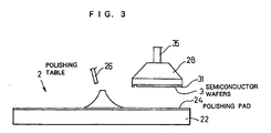
- Fig. 3 is a partial sectional view illustrating a polishing table
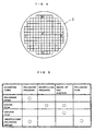
- Fig. 4 is a diagram showing a semiconductor wafer
- Fig. 5 is a chart illustrating measurement results in relation to corrective measures.
- a semiconductor wafer polishing apparatus 1 shown in Fig. 1 and Fig. 2 is constituted primarily by: polishing tables 2 for chemically and mechanically polishing the insulating films of semiconductor wafers 3 shown in Fig. 4; containers 4 for holding the semiconductor wafers 3 before polishing; moving arms 6 for holding and moving the semiconductor wafers 3 before polishing; moving arms 8 for holding and moving the semiconductor wafers 3 after polishing; a center adjuster 10 foe enabling the semiconductor wafers 3 to be held at the centers of the moving arms 6; turntables 12 which turn horizontally with the semiconductor wafers 3 mounted thereon; carriers 14 for carrying the semiconductor wafers 3 from the turntables 12 to the polishing tables 2; a measuring instrument 16 for measuring the thickness of the insulating film of the semiconductor wafer 3 before polishing; a measuring instrument 18 for measuring the thickness of the insulating film of the semiconductor wafer 3 after polishing; and containers 20 for holding the semiconductor wafers 3 after polishing.
- the polishing table 2 is composed mainly of a platen 33 which is turned by a rotating mechanism, not shown, a polishing pad 24 pasted to the top surface of the platen 22, and a supplier 26 which supplies an abrasive on the polishing pad 24 as shown in Fig. 3.
- the carrier 14 which moves longitudinally is installed above the polishing table 2, the carrier 14 being provided with a holder 28.
- the holder 28 is mounted on the carrier 14 so that it moves up and down; it has a ring 31 around it, and it is connected to a pressure regulator, not shown, to lift and hold the semiconductor wafer 3 by the negative pressure or the like of the pressure regulator.
- the holder 28 can be rotated about the axis of a shaft 35 by a driving mechanism which is not shown; it is horizontally moved back and forth and also moved up and down by the carrier 14. Hence, the semiconductor wafer 3 held by the holder 28 is pressed against the polishing table 2 while it rotates, and it is further pressed against the polishing table 2 when it moves back and forth.
- a dresser 30 for dressing the polishing surface of the polishing table 2 is installed behind the polishing table 2 as shown in Fig. 1.
- An arm assembly 31 of the dresser 30 circularly moves to dress the polishing surface while turning a dressing blade 32 in a predetermined direction.
- the moving arm 6 is composed primarily of a seat 34, a pillar 36 mounted on the seat 34, and an arm 38 rotatably installed on the pillar 36.
- the seat 34 is able to move along a travel rail 40.
- the pillar 36 extends and contracts vertically.
- the arm 38 rotates about the axis thereof and extends and contracts horizontally; it is also able to hold the semiconductor wafer 3 by using suction force produced by negative pressure which is supplied at an end section 7.
- the moving arm 8 for moving a polished semiconductor wafer has the same composition as the moving arm 6.
- the container 4 has multiple shelves to accommodate a plurality of semiconductor wafers 3, and it has a cutout on the front so as to allow the access by the end section 7 of the moving arm 6 which holds the semiconductor wafer 3.
- the center adjuster 10 is a position adjuster for matching the center of the semiconductor wafer 3 taken out of the container 4 with the center of the end section 7 of the moving arm 6.
- the turntable 12 which is rotated by a rotating mechanism, not shown, has four spots formed on the top surface thereof where the semiconductor wafers 3 are rested; two adjacent spots are for the semiconductor wafers 3 before subjected to polishing, and the remaining two adjacent spots are for the semiconductor wafers 3 after subjected to polishing.
- Washing sections 44 are installed between the turntables 12 and the polishing tables 2; the washing sections 44 wash the abrasive, etc. off the semiconductor wafers 3 which have been polished by the polishing tables 2 so as to prevent the abrasive from affecting other places.
- the measuring instrument 16 measures the thickness of the insulating film formed on the semiconductor wafer 3; it applies a beam of light to the insulating film to measure the thickness of the insulating film by the beam of light reflected by a metal layer or the like.
- the measuring instrument 16 is equipped with an image processor and a moving mechanism for moving the semiconductor wafer 3, both of which are not shown, so as to measure the thickness of the insulating film at a predetermined point of the semiconductor chip formed on the semiconductor wafer 3.
- Fig. 4 shows the examples of the measurement points of the semiconductor wafer 3.
- the chips located at four points, namely, B, C, D, and E around the center A of the semiconductor wafer 3 are selected, then the same point of each chip is selected to measure the film thickness at the same point of each chip.
- the measuring instrument 18 measures the film thickness of the semiconductor wafer 3 which has been polished; it is able to measure the film thickness of the semiconductor wafer 3 which is wet.
- the measuring instrument 18 is designed so that it is hardly affected by the abrasive remaining on the surface of the semiconductor wafer 3; it basically makes use of the interference by white light to measure the film thickness.
- the measuring instrument 18 is equipped mainly with an image recognizing device for identifying the same point of a chip formed on the semiconductor wafer, a moving table for moving a thickness sensor and an image sensor, a controller, and a computer for processing data.
- the container 20 for holding the semiconductor wafers 3 which have been polished is submerged in a water tank to submerge the semiconductor wafers 3 to prevent it from drying.
- the moving arm 8 holds the semiconductor wafer 3 which has been polished and moves it from the turntable 12 to the measuring instrument 18, the container 20, etc.
- the moving arm 6 takes out the semiconductor wafer 3 from the topmost shelf of the container 4 and carries it to the measuring instrument 16 to measure the film thickness at the center and at the same point of each of the four chips which are located orthogonally with the center of the semiconductor wafer 3.
- the measured film thickness values are sent to the controller, and the semiconductor wafer 3 which has been subjected to the measurement of the film thickness is supplied to the center adjuster 10 so as to accurately match the center thereof with the center of the end section 7 of the moving arm 6.
- the moving arm 6 sets the semiconductor wafer 3 at the pre-polishing resting location of the turntable 12.
- the turntable 12 makes a half turn to feed the semiconductor wafers 3 to the polishing table 2. Then, the holder 28 comes down to lift the semiconductor wafers 3 on the turntable 12 by suction, and the lifted semiconductor wafer 3 are moved by the carrier 14 and put on the platen 22 of the polishing table 2. On the polishing table 2, the platen 22 rotates, the abrasive is supplied from the supplier 26, and the semiconductor wafers 3 are polished by a preset polishing amount. Upon completion of the polishing operation, the carrier 14 carries the holders 28 to the washing sections 44 to remove the abrasive that has adhered to the holders 28 and the semiconductor wafers 3 during the polishing operation. After removing the abrasive, the semiconductor wafers 3 are rested at the post-polishing locations of the turntable 12.
- the turntable 12 then makes a half turn to move the semiconductor wafers 3, which have been polished, to the moving arm 8, while at the same time, the semiconductor wafers 3, which have been set at the pre-polishing resting locations of the turntable 12, are moved over to the polishing table 2.
- the moving arm 8 that handles the semiconductor wafers 3 which have been polished picks up the semiconductor wafers 3 from the turntable 12 and carries them to the measuring instrument 18.
- the measuring instrument 18 selects the locations which correspond to the locations where the measurement was performed before polishing, measures the film thickness of the semiconductor wafers 3, then sends the measurement results to the controller (not shown).
- the controller detects the state of the polished semiconductor wafer 3 according to the values of the film thickness measured before polishing and those after polishing, and compares the film thickness after polishing with the reference value. If the controller determines that the film thickness of the semiconductor wafer 3 exceeds the reference value, then it increases the polishing amount set at the polishing table 2, or if it decides that the polishing amount is too much, then it decreases the polishing amount mainly by shortening the polishing time.
- the controller determines that there are variations in the polishing amount, e.g. if the polishing surface is inclined with respect to the base of the semiconductor wafer 3, or if the polished amount at the central portion is different from that at the area around the central portion, then it changes the pressing pressure of the back surface of the holder 28 or change the condition of the polishing pad 24 by using the dresser 30.
- polished amounts Ra through Re at the points A through E of the semiconductor wafer 3 shown in Fig. 4 are measured, and polished amount Ra at the central portion is compared with a mean value Rh of the polished amounts Rb through Re around the central portion. If the result of the comparison between Ra and Rh indicates that the value of Ra is larger than Rh by a predetermined value or more, meaning that the central portion is thicker, then the controller decides that the central portion is convex; therefore, the controller increases the pressure of the back surface of the holder 28 to increase the pressure applied to the central portion. This increases the pressure applied by the holder to the central portion of the semiconductor wafer 3 to be polished after that, enabling the semiconductor wafer 3 to be provided with uniform film thickness upon completion of polishing.
- the controller sends an instruction to the dresser 30 to perform dressing to make the polishing surface of the polishing table 2 convex.
- This will correct the convex state of the film, so that uniform film thickness is accomplished after polishing, because the polishing process is based on the transfer of the configuration of the surface of the processing pad.
- an optimum configuration is created by interlocking the measuring instrument, not shown, for detecting the configuration of the polishing surface, and the dresser 30.
- the controller decides that the central portion is thinner and concave, then it sends an instruction to the dresser 30 to make the polishing surface of the polishing table 2 concave by dressing so as to correct the polishing condition thereafter.
- the controller determines a mean value Rm of the polished amounts Ra through Re at the respective points A through E in order to determine the uniformity of the polished state from the value obtained by dividing the difference between the maximum value and the minimum value of Ra through Re by Rm; or the controller determines the relationship in magnitude between Rb, Ra, and Rd on the straight line passing through point A in the central portion, and if the magnitude relationship stays constant like, for example, Rb ⁇ Ra ⁇ Rd, then it decides that there is a slope extending from point D toward point B.
- Fig. 5 shows the measurement results in relation to corrective action based on the feedback. As shown in the upper row, if the polishing speed is slow, this can be successfully handled by increasing the polishing pressure.
- the backfilling pressure is increased or the configuration of the pad surface is readjusted to make correction; or if the film is concave, then the configuration of the pad surface is corrected. If the polishing amount is insufficient, the polishing amount is corrected.
- the semiconductor wafer 3 which has been subjected to the measurement of the film thickness is moved by the moving arm 8 and placed in the container 20.
- the semiconductor wafers 3 which have been polished are placed in the container 20, they are submerged in water to prevent them from drying.
- the container is filled up with the semiconductor wafers 3, it is replaced by the container 20 that is empty.
- the semiconductor wafer polishing apparatus 1 in accordance with the present invention measures the film thickness of the semiconductor wafer 3 at the predetermined locations by the measuring instrument 16 before starting polishing the semiconductor wafer 3, measures the film thickness again at the locations corresponding to the locations, where the measurement was performed before polishing, after completion of the polishing operation by the polishing table 2, determines the polishing condition of the polishing apparatus 1 according to the obtained measurement results, and changes the polishing condition as necessary. Hence, a desired polishing condition can be maintained and accurate polishing can be continued without waste.
- a film thickness measuring unit is installed outside the semiconductor wafer polishing apparatus 1 so that the film thickness of the semiconductor wafer 3 before starting the polishing operation is measured by the film thickness measuring unit installed outside.
- the measurement result given by this external measuring unit is supplied to the semiconductor wafer polishing apparatus 1; the polished state of the semiconductor wafer 3 on the semiconductor wafer polishing apparatus 1 is determined according to the measurement result supplied before polishing and the measurement result obtained after polishing so as to change the polishing condition as necessary. This also makes it possible to immediately determine the polished state and to achieve proper setting based on the determined polished state, thus enabling accurate, continuous polishing of the semiconductor wafer 3.
- the insulating film has been polished, however, the present invention is not limited thereto.
- the measuring instruments for measuring the film thickness of a semiconductor wafer before and after polishing are provided, and the polishing conditions and the like are adjusted according to the measurement results given by the measuring instruments. Hence, appropriate polishing condition can be grasped, and the semiconductor wafers can be accurately polished in succession according to the measurement results.
- the semiconductor wafer polishing apparatus is intended to effect polishing the surface of a semiconductor wafer with difference in level for smoothing. Prior to the polishing, film thickness of the semiconductor wafer is measured and then amount of polishing of the semiconductor wafer is determined on the basis of the measurement result at any time for polishing. Thus it is possible to effect appropriate polishing of the semiconductor wafer by required amount.
Landscapes
- Engineering & Computer Science (AREA)
- Mechanical Engineering (AREA)
- Physics & Mathematics (AREA)
- Condensed Matter Physics & Semiconductors (AREA)
- General Physics & Mathematics (AREA)
- Manufacturing & Machinery (AREA)
- Computer Hardware Design (AREA)
- Microelectronics & Electronic Packaging (AREA)
- Power Engineering (AREA)
- Mechanical Treatment Of Semiconductor (AREA)
- Finish Polishing, Edge Sharpening, And Grinding By Specific Grinding Devices (AREA)
- Testing Or Measuring Of Semiconductors Or The Like (AREA)
Applications Claiming Priority (3)
| Application Number | Priority Date | Filing Date | Title |
|---|---|---|---|
| JP24972796A JPH1098016A (ja) | 1996-09-20 | 1996-09-20 | 半導体ウェハ研磨装置 |
| JP24972796 | 1996-09-20 | ||
| PCT/JP1997/003341 WO1998012739A1 (fr) | 1996-09-20 | 1997-09-19 | Polissoir pour plaquette a semi-conducteurs |
Publications (2)
| Publication Number | Publication Date |
|---|---|
| EP1017090A1 true EP1017090A1 (fr) | 2000-07-05 |
| EP1017090A4 EP1017090A4 (fr) | 2000-07-05 |
Family
ID=17197312
Family Applications (1)
| Application Number | Title | Priority Date | Filing Date |
|---|---|---|---|
| EP97940435A Withdrawn EP1017090A4 (fr) | 1996-09-20 | 1997-09-19 | Polissoir pour plaquette a semi-conducteurs |
Country Status (5)
| Country | Link |
|---|---|
| EP (1) | EP1017090A4 (fr) |
| JP (1) | JPH1098016A (fr) |
| KR (1) | KR20000036250A (fr) |
| TW (1) | TW344107B (fr) |
| WO (1) | WO1998012739A1 (fr) |
Cited By (5)
| Publication number | Priority date | Publication date | Assignee | Title |
|---|---|---|---|---|
| WO2004003470A1 (fr) * | 2002-06-26 | 2004-01-08 | Nova Measuring Instruments Ltd. | Procede et systeme de mesure de films minces |
| US7732332B2 (en) * | 2006-03-10 | 2010-06-08 | United Microelectronics Corp. | Chemical mechanical polishing method with inspection pre and post processing |
| CN107851579A (zh) * | 2015-05-29 | 2018-03-27 | 太阳能爱迪生半导体有限公司 | 用于处理具有多晶磨光的半导体晶片的方法 |
| US11688653B2 (en) | 2020-03-06 | 2023-06-27 | Kioxia Corporation | Semiconductor manufacturing apparatus and method of manufacturing semiconductor device |
| CN114102269B (zh) * | 2015-05-29 | 2024-09-24 | 环球晶圆股份有限公司 | 用于处理具有多晶磨光的半导体晶片的方法 |
Families Citing this family (5)
| Publication number | Priority date | Publication date | Assignee | Title |
|---|---|---|---|---|
| JPH11204468A (ja) * | 1998-01-09 | 1999-07-30 | Speedfam Co Ltd | 半導体ウエハの表面平坦化装置 |
| JP2003124171A (ja) | 2001-10-19 | 2003-04-25 | Nec Corp | 研磨方法および研磨装置 |
| KR100641489B1 (ko) * | 2003-12-30 | 2006-10-31 | 동부일렉트로닉스 주식회사 | 씨엠피 장비와 그 작동 방법 |
| KR100914578B1 (ko) * | 2007-12-12 | 2009-08-31 | 주식회사 실트론 | 웨이퍼 가공장치 및 이를 이용한 웨이퍼 가공방법 |
| KR102203419B1 (ko) * | 2013-12-09 | 2021-01-15 | 주식회사 케이씨텍 | 화학 기계적 연마 방법 및 장치 |
Family Cites Families (2)
| Publication number | Priority date | Publication date | Assignee | Title |
|---|---|---|---|---|
| US5081796A (en) * | 1990-08-06 | 1992-01-21 | Micron Technology, Inc. | Method and apparatus for mechanical planarization and endpoint detection of a semiconductor wafer |
| JPH07285069A (ja) * | 1994-04-18 | 1995-10-31 | Shin Etsu Handotai Co Ltd | 枚葉式研磨におけるウェーハのテーパ自動除去研磨方法と装置 |
-
1996
- 1996-09-20 JP JP24972796A patent/JPH1098016A/ja not_active Withdrawn
-
1997
- 1997-09-19 EP EP97940435A patent/EP1017090A4/fr not_active Withdrawn
- 1997-09-19 KR KR1019997002343A patent/KR20000036250A/ko not_active Application Discontinuation
- 1997-09-19 TW TW086113653A patent/TW344107B/zh active
- 1997-09-19 WO PCT/JP1997/003341 patent/WO1998012739A1/fr not_active Application Discontinuation
Non-Patent Citations (2)
| Title |
|---|
| No further relevant documents disclosed * |
| See also references of WO9812739A1 * |
Cited By (17)
| Publication number | Priority date | Publication date | Assignee | Title |
|---|---|---|---|---|
| WO2004003470A1 (fr) * | 2002-06-26 | 2004-01-08 | Nova Measuring Instruments Ltd. | Procede et systeme de mesure de films minces |
| US7327476B2 (en) | 2002-06-26 | 2008-02-05 | Nova Measuring Instruments Ltd. | Thin films measurement method and system |
| US7595896B2 (en) | 2002-06-26 | 2009-09-29 | Nova Measuring Instruments Ltd. | Thin films measurement method and system |
| US8040532B2 (en) | 2002-06-26 | 2011-10-18 | Nova Measuring Instruments Ltd. | Thin films measurement method and system |
| US8564793B2 (en) | 2002-06-26 | 2013-10-22 | Nova Measuring Instruments Ltd. | Thin films measurement method and system |
| US7732332B2 (en) * | 2006-03-10 | 2010-06-08 | United Microelectronics Corp. | Chemical mechanical polishing method with inspection pre and post processing |
| EP3576136A1 (fr) * | 2015-05-29 | 2019-12-04 | GlobalWafers Co., Ltd. | Procédé de polissage d'une tranche semi-conductrice |
| US20180151384A1 (en) * | 2015-05-29 | 2018-05-31 | Sunedison Semiconductor Limited | Methods for processing semiconductor wafers having a polycrystalline finish |
| CN107851579A (zh) * | 2015-05-29 | 2018-03-27 | 太阳能爱迪生半导体有限公司 | 用于处理具有多晶磨光的半导体晶片的方法 |
| US10699908B2 (en) | 2015-05-29 | 2020-06-30 | Globalwafers Co., Ltd. | Methods for processing semiconductor wafers having a polycrystalline finish |
| TWI714591B (zh) * | 2015-05-29 | 2021-01-01 | 環球晶圓股份有限公司 | 用於處理具有多晶磨光之半導體晶圓之方法 |
| TWI742938B (zh) * | 2015-05-29 | 2021-10-11 | 環球晶圓股份有限公司 | 用於處理具有多晶磨光之半導體晶圓之方法 |
| CN107851579B (zh) * | 2015-05-29 | 2021-11-09 | 环球晶圆股份有限公司 | 用于处理具有多晶磨光的半导体晶片的方法 |
| CN114102269A (zh) * | 2015-05-29 | 2022-03-01 | 环球晶圆股份有限公司 | 用于处理具有多晶磨光的半导体晶片的方法 |
| US11355346B2 (en) * | 2015-05-29 | 2022-06-07 | Globalwafers Co., Ltd. | Methods for processing semiconductor wafers having a polycrystalline finish |
| CN114102269B (zh) * | 2015-05-29 | 2024-09-24 | 环球晶圆股份有限公司 | 用于处理具有多晶磨光的半导体晶片的方法 |
| US11688653B2 (en) | 2020-03-06 | 2023-06-27 | Kioxia Corporation | Semiconductor manufacturing apparatus and method of manufacturing semiconductor device |
Also Published As
| Publication number | Publication date |
|---|---|
| KR20000036250A (ko) | 2000-06-26 |
| EP1017090A4 (fr) | 2000-07-05 |
| TW344107B (en) | 1998-11-01 |
| JPH1098016A (ja) | 1998-04-14 |
| WO1998012739A1 (fr) | 1998-03-26 |
Similar Documents
| Publication | Publication Date | Title |
|---|---|---|
| US7989348B2 (en) | Polishing method and polishing apparatus | |
| US6659842B2 (en) | Method and apparatus for optical monitoring in chemical mechanical polishing | |
| EP0914908A2 (fr) | Procédé et dispositif de polissage | |
| US7400934B2 (en) | Methods and apparatus for polishing control | |
| US5830041A (en) | Method and apparatus for determining endpoint during a polishing process | |
| EP1543921A1 (fr) | Procédé et appareil de polissage pour plaquettes semi-conductrices | |
| US6905400B2 (en) | Method and apparatus for dressing polishing cloth | |
| US6113465A (en) | Method and apparatus for improving die planarity and global uniformity of semiconductor wafers in a chemical mechanical polishing context | |
| US6929531B2 (en) | System and method for metal residue detection and mapping within a multi-step sequence | |
| JP2003511873A (ja) | 半導体ウェハ研磨方法およびシステム | |
| US6387807B1 (en) | Method for selective removal of copper | |
| US7074109B1 (en) | Chemical mechanical polishing control system and method | |
| KR20180115858A (ko) | 기판 처리 장치 및 그 제어방법 | |
| EP1017090A1 (fr) | Polissoir pour plaquette a semi-conducteurs | |
| JP4259048B2 (ja) | コンディショナの寿命判定方法及びこれを用いたコンディショナの判定方法、研磨装置、並びに半導体デバイス製造方法 | |
| US7166015B2 (en) | Apparatus and method for controlling fluid material composition on a polishing pad | |
| JP2004047876A (ja) | 研磨装置及び研磨方法 | |
| US6254457B1 (en) | Process for polishing wafers of integrated circuits | |
| US6991516B1 (en) | Chemical mechanical polishing with multi-stage monitoring of metal clearing | |
| TWI729712B (zh) | 研削裝置及研削方法 | |
| JPS5815265B2 (ja) | 自動形状修正研摩装置 | |
| JP3019849B1 (ja) | 化学的機械的研磨装置 | |
| US20040214508A1 (en) | Apparatus and method for controlling film thickness in a chemical mechanical planarization system | |
| JPH08174417A (ja) | 研磨装置及び研磨量制御方法 |
Legal Events
| Date | Code | Title | Description |
|---|---|---|---|
| PUAI | Public reference made under article 153(3) epc to a published international application that has entered the european phase |
Free format text: ORIGINAL CODE: 0009012 |
|
| 17P | Request for examination filed |
Effective date: 19990318 |
|
| A4 | Supplementary search report drawn up and despatched |
Effective date: 19991116 |
|
| AK | Designated contracting states |
Kind code of ref document: A4 Designated state(s): DE FR GB IT Kind code of ref document: A1 Designated state(s): DE FR GB IT |
|
| RAP1 | Party data changed (applicant data changed or rights of an application transferred) |
Owner name: SPEEDFAM-IPEC INC. |
|
| STAA | Information on the status of an ep patent application or granted ep patent |
Free format text: STATUS: THE APPLICATION IS DEEMED TO BE WITHDRAWN |
|
| 18D | Application deemed to be withdrawn |
Effective date: 20040401 |