EP1016218B1 - Phasendetektor zur taktrückgewinnung von datensignalen - Google Patents
Phasendetektor zur taktrückgewinnung von datensignalen Download PDFInfo
- Publication number
- EP1016218B1 EP1016218B1 EP98913483A EP98913483A EP1016218B1 EP 1016218 B1 EP1016218 B1 EP 1016218B1 EP 98913483 A EP98913483 A EP 98913483A EP 98913483 A EP98913483 A EP 98913483A EP 1016218 B1 EP1016218 B1 EP 1016218B1
- Authority
- EP
- European Patent Office
- Prior art keywords
- signal
- phase
- circuit
- divided
- phase detector
- Prior art date
- Legal status (The legal status is an assumption and is not a legal conclusion. Google has not performed a legal analysis and makes no representation as to the accuracy of the status listed.)
- Expired - Lifetime
Links
Images


Classifications
-
- H—ELECTRICITY
- H03—ELECTRONIC CIRCUITRY
- H03L—AUTOMATIC CONTROL, STARTING, SYNCHRONISATION OR STABILISATION OF GENERATORS OF ELECTRONIC OSCILLATIONS OR PULSES
- H03L7/00—Automatic control of frequency or phase; Synchronisation
- H03L7/06—Automatic control of frequency or phase; Synchronisation using a reference signal applied to a frequency- or phase-locked loop
- H03L7/08—Details of the phase-locked loop
- H03L7/085—Details of the phase-locked loop concerning mainly the frequency- or phase-detection arrangement including the filtering or amplification of its output signal
- H03L7/089—Details of the phase-locked loop concerning mainly the frequency- or phase-detection arrangement including the filtering or amplification of its output signal the phase or frequency detector generating up-down pulses
- H03L7/0891—Details of the phase-locked loop concerning mainly the frequency- or phase-detection arrangement including the filtering or amplification of its output signal the phase or frequency detector generating up-down pulses the up-down pulses controlling source and sink current generators, e.g. a charge pump
- H03L7/0893—Details of the phase-locked loop concerning mainly the frequency- or phase-detection arrangement including the filtering or amplification of its output signal the phase or frequency detector generating up-down pulses the up-down pulses controlling source and sink current generators, e.g. a charge pump the up-down pulses controlling at least two source current generators or at least two sink current generators connected to different points in the loop
-
- H—ELECTRICITY
- H03—ELECTRONIC CIRCUITRY
- H03D—DEMODULATION OR TRANSFERENCE OF MODULATION FROM ONE CARRIER TO ANOTHER
- H03D13/00—Circuits for comparing the phase or frequency of two mutually-independent oscillations
- H03D13/003—Circuits for comparing the phase or frequency of two mutually-independent oscillations in which both oscillations are converted by logic means into pulses which are applied to filtering or integrating means
- H03D13/004—Circuits for comparing the phase or frequency of two mutually-independent oscillations in which both oscillations are converted by logic means into pulses which are applied to filtering or integrating means the logic means delivering pulses at more than one terminal, e.g. up and down pulses
-
- H—ELECTRICITY
- H03—ELECTRONIC CIRCUITRY
- H03L—AUTOMATIC CONTROL, STARTING, SYNCHRONISATION OR STABILISATION OF GENERATORS OF ELECTRONIC OSCILLATIONS OR PULSES
- H03L7/00—Automatic control of frequency or phase; Synchronisation
- H03L7/06—Automatic control of frequency or phase; Synchronisation using a reference signal applied to a frequency- or phase-locked loop
- H03L7/08—Details of the phase-locked loop
- H03L7/085—Details of the phase-locked loop concerning mainly the frequency- or phase-detection arrangement including the filtering or amplification of its output signal
-
- H—ELECTRICITY
- H04—ELECTRIC COMMUNICATION TECHNIQUE
- H04L—TRANSMISSION OF DIGITAL INFORMATION, e.g. TELEGRAPHIC COMMUNICATION
- H04L7/00—Arrangements for synchronising receiver with transmitter
- H04L7/02—Speed or phase control by the received code signals, the signals containing no special synchronisation information
- H04L7/033—Speed or phase control by the received code signals, the signals containing no special synchronisation information using the transitions of the received signal to control the phase of the synchronising-signal-generating means, e.g. using a phase-locked loop
Definitions
- the present invention relates to the field of data communications, clock recovery, clock recovery of non-self clocking signals, phase-locked loop clock recovery, phase detectors, and monolithic phase detectors.
- the present invention is a phase detector, suitable for monolithic implementation, for use in a high speed phase-locked loop clock recovery system for non-return-to-zero data signals.
- Serial digital transmission of non-self clocking or non-retum-to-zero (NRZ) binary signals requires receiving circuitry to extract timing infonnation from the serial data to regenerate the clock. This recovered clock is used to re-time the serial data for subsequent circuitry to receive and process it synchronously.
- the PLL contains a voltage-controlled oscillator (VCO) which is controlled by an integrated and low pass filtered output of a phase detector.
- the phase detector output is representative of the phase difference between the input serial data and the recovered clock, the latter being equal to or derived from the VCO output.
- the phase difference between an input NRZ data signal and a locally generated clock signal can be obtained by generating a variable control pulse signal proportional in width to that phase difference, in addition to one or more other fixed width control pulses.
- the control pulses are fed to control circuitry, such as a charge pump, which yields a phase detector output signal.
- the phase detector output signal is filtered and integrated to produce a phase error voltage signal which is then used to drive the VCO.
- a phase detector such as this was disclosed in U.S. Patent No. 4,535,459 by Hogge and modified in U.S. Patent No. 5,027,085 by DeVito to reduce phase jitter caused by variations in data density.
- phase of the VCO output signal will only remain the same, before and after a series of changes in the VCO input signal, if the average value of those changes is zero (or equivalently if the average value of the integrated phase detector output signal does not change).
- a phase detector for this application must generate phase difference information only when input data transitions occur. Ideally, the falling edge of the clock coincides with a data transition, so that the data is phase aligned for the rising edge of the clock to retime the data in the centre of the data interval. This condition ensures the most stable and reliable reading-in of the data. When it occurs there is said to be zero phase error, and the phase of the VCO output should not change. Phase jitter, which consists of spurious variations in the phase of the regenerated clock signal must therefore be minimized.
- phase detector circuits may provide zero static phase offset, they do not provide zero phase offset in high speed applications where the input serial data itself has significant jitter (with respect to the clock) and where practical circuitry and subsequent circuitry have limited bandwidth. The result is a reduction in input jitter tolerance. It is therefore an object of the present invention to provide a phase detector circuit which provides minimal static phase offset in the presence of large input jitter, increases the input jitter tolerance, and allows for the use of circuitry with lower bandwidth and therefore with lower current consumption.
- phase detector of the invention is defined in the appended claims.
- Fig. 1 shows a basic circuit block diagram for a phase-locked loop (PLL) 2 used to recover or regenerate a clock signal 12 from input serial NRZ data 10.
- the phase detector circuitry 4 provides a plurality of control pulse signals 5 to the control (summing) circuitry 6 which outputs a phase detector output signal 50 in response.
- the phase detector output 50 is the input to loop filter and integrator 7.
- the output 9 of loop filter 7 is the phase error voltage signal which drives a voltage controlled oscillator (VCO) 8 whose output is essentially the recovered clock signal 12 which is fed back to gate (i.e. control the timing of) the phase detector circuitry 4.
- VCO voltage controlled oscillator
- Figs. 2A and 2B show two versions of the prior art phase detector circuit disclosed by Devito in U.S. Patent No. 5,027,085.
- an input data signal 10 is connected to the input of a delay or retiming means 14, whose output 22 is connected to the input of a delay or retiming means 16, whose output 24 is in turn connected to the input of a delay or retiming means 18.
- the retiming means 14, 16, and 18 are all gated by alternate edges or levels (depending on the type of retiming means used) of the regenerated clock signal 12, which is derived from the phase detector output 50.
- Fig. 1 shows two versions of the prior art phase detector circuit disclosed by Devito in U.S. Patent No. 5,027,085.
- an input data signal 10 is connected to the input of a delay or retiming means 14, whose output 22 is connected to the input of a delay or retiming means 16, whose output 24 is in turn connected to the input of a delay or retiming means
- the retiming means 14, 16, and 18 are shown as D flip-flops and so are triggered by either the rising or falling edges of the regenerated clock signal 12. As shown in Fig. 2A, D flip-flops 14 and 18 are rising-edge triggered and D flip-flop 16 is falling edge triggered.
- the retiming means could also each consist of a master and slave combination of two D latches. It is obvious to those skilled in the art that the slave latch of one retiming means can perform the dual role of master latch in the next retiming means, thus allowing for the omission of redundant latches. In this manner, the retiming means 14, 16, and 18 can consist of a "series" combination of 4 latches.
- the control pulse signals UP1 38, DOWN 40, and UP2 42 are generated by exclusive-OR (XOR) gates 30, 32, and 34 respectively.
- the inputs to XOR gate 30 are the input data signal 10 and the output 22 of retiming means 14.
- the inputs to XOR gate 32 are the output 22 of retiming means 14 and the output 24 of retiming means 16.
- the inputs to XOR gate 30 are the output 24 of retiming means 16 and the output 26 of retiming means 18.
- the DOWN signal 40 is doubled at the multiplier 46.
- the UP1 signal 38 and the UP2 signal 42 are summed positively and the DOWN signal 40 is summed negatively.
- the output of the summer is the phase detector output 50 from which the regenerated clock signal 12 is derived.
- the circuit of Fig. 2B shows the phase detector of Fig. 2A with an additional retiming means 20 whose input is the output 26 of retiming means 18.
- a fourth control pulse signal 44 is generated by XOR gate 36 whose inputs are the output 26 of retiming means 18 and the output of retiming means 20. The presence of an additional control signal 44 obviates the requirement of doubling the DOWN control signal 40 before summing.
- Fig. 3 shows a timing diagram for the operation of the circuit of FIG. 2A.
- the data (or bit) rate for signal 10 is lower than the frequency of the clock signal 12.
- the clock signal 12 is also shown as a constant frequency and phase signal. In operation, however, the clock signal will change in response to the phase detector output signal 50 when the time average of the changes in the filtered and integrated phase detector output signal (the phase error signal) is non-zero.
- the UP1 pulses can vary in pulse width between zero and one period of the clock signal 12. As the input data lags the clock, the positive UP1 pulses become more and more narrow. In practical XOR gates and control circuits, such as charge pumps, there is a limit for the response time of the circuit which results in effectively narrowing or eliminating input pulses which are too narrow. Therefore, as the UP1 pulses become narrower and narrower, they are ultimately filtered out and do not provide any pulse information for driving the VCO. In such cases and also in the case of high speed applications, the phase detector transfer function has a non-linearity which is shown in Fig. 4. As described below, this non-linearity can cause a significant reduction in input jitter tolerance for the phase detector circuits of Figs. 2A and 2B.
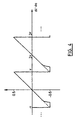
- Fig. 5 illustrates the low pass filtered time response of the non-linear phase detector transfer function to an input in which the data rate equals the clock frequency and the two signals have a sinusoidal phase difference 54.
- the non-linear distortion 56 results in an average negative phase detector output.
- the PLL circuit responds by decreasing the phase of the VCO output or clock until the average phase error is zero. As a result, a phase offset will occur in the presence of large input jitter, which, in turn, translates into a reduction in input jitter tolerance.
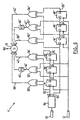
- Figs. 6 through 12 show several possible embodiments of a phase detector circuit 4' of the present invention.
- the input serial data is initially frequency divided by two, resulting in an "in-phase" data signal I and a data signal Q in "phase quadrature" with the input signal 10.
- Fig. 13 shows an example of a circuit 64 which performs the dividing function via latches 66 and 68
- Fig. 14 is a timing diagram of the signals involved, ignoring propagation delays.
- the signals I 60 and Q 62 effectively contain every other data transition from the input signal 10.
- the data signal I 60 toggles at each rising edge of the signal 10, and the data signal Q 62 toggles at each falling edge of the signal 10, so that when the signal 10 is low I and Q are at the same level and when the signal 10 is high I and Q are at different levels.
- the original input data signal can be regenerated by an XOR function of the two divided data signals, as shown at 64 in Fig. 11.
- the input serial data could also be frequency divided by an integral number greater than two and then recombined in a manner similar to that just described.
- a first embodiment of the present invention which divides at 64 the input signal 10 and then processes each divided signal 60 and 62 through a series of retiming means, shown in Fig. 6 as flip-flops.
- the independent processing of each divided 60 and 62 signal is similar to the processing of the complete input data signal 12 which took place in Fig. 2A.
- the signal Q 62 passes through three retiming means 14', 16', and 18' and generates three control pulse signals 38', 40' and 42' via XOR gates 30', 32', and 34'.
- the signal I 60 passes through another three retiming means 14", 16", and 18" and generates three control pulse signals 38", 40" and 42" via XOR gates 30", 32", and 34".
- the retiming means are gated by alternate edges (if the retiming means are flip-flops) or alternate levels (if the retiming means are slave-latch combinations) of the clock signal 12. Corresponding retiming means in each processing stream are similarly gated. For example and as shown in Fig. 6, the flip-flops 14', 14", 18', and 18" are rising edge triggered and the flip-flops 16' and 16" are falling edge triggered.
- the inputs to the XOR gate 30' are the signal Q 62 and the output 24' of the retiming means 16'.
- the inputs to the XOR gate 30" are the signal I 60 and the output 24" of the retiming means 16".
- the signals 38' and 38" have a minimum pulse width of one half of a clock period. Due to the lengthening of the 38' and 38" pulses the multipliers 46' and 46" multiply by three as compared to by two in Fig 2A. The resolution of control signal pulses for consecutive data transitions in the input signal 10 remains possible, in spite of the lengthening of the pulse widths of signals 38' and 38", because of the initial frequency division of that signal.
- the phase detector circuit of Fig. 6 can be reduced to the circuit of Fig. 7, as will be obvious to one skilled in the art.
- the once retimed data input signal 22 is produced or recombined by an XOR function at 70 of the once retimed divided input signals 22' and 22".
- the twice retimed data input signal 24 is produced or recombined by an XOR function at 72 of the twice retimed divided input signals 24' and 24". This allows retiming means 18 and XOR gates 32 and 34 to function as already described in Fig. 2A.
- the XOR gate 74 is necessary to match the propagation delay of XOR gate 72 (so that the width of control pulse 42 is one-half a clock period, with the accuracy of that value depending on the matching of the delay through gates 72 and 74), but otherwise XOR gate 74 does not affect the functionality of the phase detector circuit.
- Fig. 8 shows a similar embodiment to the circuit of Fig. 7 where an additional retiming means is added in the same manner that the circuit of Fig. 2A was extended into the circuit of Fig. 2B, as already described above.
- Fig. 9 shows the phase detector circuit of Fig. 7 implemented with gated D-type latches replacing the flip-flops of Fig. 7 as the retiming means, in the manner explained above.
- latch 92 acts as a slave latch to both latches 84 and 90.
- Other similar functional implementations, such as of the circuits of Fig. 6 or 8 with gated D-type latches replacing the flip-flops as retiming means, will be obvious to those skilled in the art.
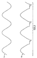
- Fig. 15 shows the output waveforms for the circuit of Fig. 9.
- Three UP signals 38', 38", and 42 and one DOWN signal 40 are summed to produce the phase detector output 50.
- UP1 38' is produced on every other input data signal transition
- UP2 38" is produced on all other data transitions. Since the occurrence of the UP1 38' or UP2 38" signal is half the frequency of that of the prior art (see signal 38 in Fig.
- the XOR gate 72 in Fig. 7, 8 or 9 can also be replaced with an appropriately gated retiming means with its input connected to the output of XOR gate 70 (signal 22), its output connected to the input to flip flop 18 in Figs. 7 and 8 or to latch 92 in Fig. 9 (signal 24), and its clock input connected to the output of XOR gate 74.
- Fig. 10 shows such an implementation for the circuit of Fig. 9 with the XOR gate 72 replaced by the latch 91.
- XOR gate 74 matches the delay through the XOR gate 70.
- Delay means 96, 98, 100, and 102 are also added to the circuit of Fig. 10 to correct for the set-up time and propagation delay of the latches 80, 82, 86, and 88.
- Delay means 96 and 98 each provide for a delay equivalent to one data latch and may consist of a permanently enabled data latch.
- Delay means 100 and 102 each provide for a delay equivalent to two data latches and may consist of a combination of two permanently enabled data latches.
- Delay means 96, 98, 100, and 102 can be added to the circuits of Figs. 6 through 9 in the same manner as illustrated in Fig. 10 to correct for the inherent delays present in the retiming means of those circuits. With these delay means added to it, the circuit of Fig. 9 is functionally equivalent to the circuit of Fig. 10.
- the circuit of Fig. 10 can be reduced to the circuit of Fig. 11 in which latch 92 is removed and only two retimings of the input data signal 10 effectively take place.
- the XOR gates 32' and 32" perform the same function as the identically labelled gates in Fig. 6 in generating signals 40' and 40" respectively.
- the DOWN signal 40 is generated by an OR function at gate 104 of the signals 40' and 40".
- phase of the VCO output should not change, and therefore the average value of the phase error signal or VCO input (i.e. the filtered and integrated phase detector output signal) should not change.
- the average change in the phase detector output signal 50 in response to an input data transition may be zero
- the average change in the integrated phase detector output (the phase error signal 9 in Fig. 1) may still be non-zero.
- This concept is illustrated by way of example in Figs. 16A and 16B.
- phase detector outputs such as that shown in Fig. 16A, a non-zero phase offset will result when there are variations in the density of input data transitions. This "pattern dependent jitter" may occur in wideband systems.
- phase detector circuit of Fig. 11 does suffer from this drawback.
- the phase detector circuit of Fig. 11 is further modified into the circuit of Fig. 12.
- the OR gate 104 (and the delay through it) is removed and the summing of the DOWN pulses 40' (DOWN1) and 40" (DOWN2) takes place at the control summing circuit 6.
- Delay means 104 and 106 each providing a delay of one-quarter of the clock period are also added to delay the arrival of the UP1 and UP2 signals at the summing circuit 6 relative to the DOWN pulses.
- the phase detector circuit of Fig. 12 is advantageous when a phase detector circuit is to be used in a single clock frequency PLL system, since the delays 104 and 106 are fixed value delays which are easily implemented.
- the circuit of Fig. 12 may also be used in a multi-clock frequency PLL system, but the delay means 104 and 106 are variable and therefore more complex.
- Fig. 17 shows the output waveforms for the circuit of Fig. 12.
- the circuit is phase-locked (i.e. there is no phase error) the corresponding UP and DOWN pulses overlap so that the phase detector output pulses one unit high for one-quarter clock period, pulses one unit low for one-half clock period, and pulses one unit high again for one-quarter clock period.
- a phase locked phase detector output pulses one unit high for one-half clock period, pulses two units low for one-half clock period, and pulses one unit high for one-half clock period.
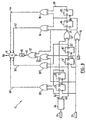
- the complete phase detector for the preferred embodiment in Fig. 12 with charge pump control circuitry 6 is shown in a phase-locked loop in Fig. 18.
- the control pulse (UP and DOWN) signals are used to control, by way of switches 120, 122, 124, and 126, the charge pump 6 which comprises current sources 112, 114, 116 and 118 working into a loop filter 7 which processes the phase detector output signal and which may comprise a resistor-capacitor network.
- the filter 7 achieves both the integration of the current signal pulses and a low pass filter function to define the PLL bandwidth.
- the switches 120, 122, 124, and 126 in the charge pump 6 have limited bandwidth and thus require control pulses of some minimum width.
- the summing function is simply the connection of the current sources into one common node 110 where the loop filter 7 is connected. Although node 110 is shown as single-ended, the specific configuration, whether single-ended or differential, is not significant. Similar charge pump summation circuitry can be implemented for any embodiments of the present invention.
- the charge pump 6 receives a net positive (or UP) pulse when the clock lags the input serial data and dumps a net positive charge packet into the resistor-capacitor network (loop filter) 7 to increase the VCO frequency. Where no input serial data transitions occur, no charge is added or removed from the loop filter 7, and the VCO frequency remains unchanged. Therefore, only when input data transitions occur, does the phase detector provide control signal pulses of net width proportional to the phase difference of the input data and clock signals.
- the feedback of the PLL 2 will force the pulse widths of UP1 38' and UP2 38" to equal twice that of the DOWN1 and DOWN2 pulses 40' and 40" (for example, at 108 in Fig. 17.)
- the width of the DOWN pulses is one-half the clock period, and the accuracy of that value depends on the matching of the delay from the clock input to the output of D latches 82 and 84 for DOWN1 and from the clock input to the output of D latches 86 and 88 for DOWN2.
- the width of UP1 and UP2 depend on the matching of the gate delays for the arrival of each of the inputs to XOR gates 30' and 30" respectively, and are determined by the time from a data transition to a positive clock edge plus one-half a clock period. Therefore, the PLL 2 locks when the time from a data transition to a positive clock edge equals one-half a clock period.
- the value of Iup1 112 and Iup2 114 must equal one-half the value of Idown1 116 and Idown2 118 to ensure the condition of zero static phase offset.
- the clock output 76 is synchronized to the regenerated data 78 (Data Out) so that the positive edge of the clock occurs one-half a data bit-period after the data transition.
- the present invention is not limited to embodiments which frequency divide the input data signal by two but rather may generally include frequency division of the input by an integer N which is greater than two, so as to provide a plurality of N divided signals.
- the number of divided signals N is a positive integer power of two (i.e. N equals 2 M where M is a positive integer so that N may equal 2, 4, 8, etc.) since the N divided signals may then be obtained by further dividing each signal in a preceding set of divided signals (until the required number of divided signals is obtained) in the same manner that the initial set of divided signals was obtained.
- the widths of the control pulses are lengthened, it will be necessary to frequency divide the input signal by a number greater than two in order to ensure the resolution of consecutive data transitions in the input signal.
Landscapes
- Engineering & Computer Science (AREA)
- Power Engineering (AREA)
- Stabilization Of Oscillater, Synchronisation, Frequency Synthesizers (AREA)
- Manipulation Of Pulses (AREA)
- Synchronisation In Digital Transmission Systems (AREA)
Claims (8)
- Phasendetekiorschaltung (4,4') zum Erfassen der Phasendifferenz zwischen einem Informationssignal (10) und einem Taktsignal (12), wobei das Taktsignal und das Informationssignal impulsartige Wellenformen mit einem ersten und zweiten Pegel und einer ersten und zweiten Flanke sind, wobei das Informationssignal Daten bei einer bestimmten Datenrate enthält, und die erste und zweite Flanke des Informationssignals Übergänge sind, der Phasendetektor eine mit einer Impulssignalschaltung (14', 16', 18', 14", 16", 18", 30', 32', 34', 30", 32", 34") verbundene Phasenfehlersignalschaltung (6) umfasst, die als Reaktion auf eine Vielzahl von Steuerimpulssignalen (38', 40', 42', 38", 40", 42") ein Phasenfehlersignal (9) erzeugt, wobei das Phasenfehlersignal (9) die Phasendifferenz darstellt, dadurch gekennzeichnet, dass die Phasendetektorschaltung (4, 4') des Weiteren umfasst:(a) eine Teilerschaltung (64) zum Teilen des Informationssignals (10) in ein erstes geteiltes Signal (60) und ein zweites geteiltes Signal (62), wobei die Datenrate des ersten geteilten Signals (60) und des zweiten geteilten Signals (62) eine Hälfte der Datenrate des Informationssignals ist, und(b) die mit der Teilerschaltung (64) und der Phasenfehlersignalschaltung (6) verbundene Impulssignalschaltung, wobei die Impulssignalschaltung eine erste Schaltung, die eine erste Vielzahl von Retiming-Elementen (14', 16', 18') enthält, die mit einer ersten Vielzahl von XOR-Gattern (30', 32', 34') zusammengeschaltet sind, und eine zweite Schaltung umfasst, die eine zweite Vielzahl von Retiming-Elementen (14", 16", 18") enthält, die mit einer zweiten Vielzahl von XOR-Gattern (30", 32", 34") zusammengeschaltet sind, wobei die erste und zweite Vielzahl von XOR-Gattern Steuerimpulssignale (38', 40', 42', 38", 40", 42") erzeugen, wobei jedes der Steuerimpulssignale auf die Phasendifferenz zwischen dem ersten (60) oder dem zweiten geteilten Signal (62) und dem Taktsignal (12) anspricht
- Phasendetektorschaltung nach Anspruch 1, wobei die Phasenfehlersignalschaltung (6) umfasst:(a) eine erste schaltbare Stromquelle (112, 120), die als Reaktion auf ein erstes Steuerimpulssignal (38') arbeitet und zwischen einen gemeinsamen Knoten (110) und einen Referenzknoten geschaltet ist;(b) eine zweite schaltbare Stromquelle (114, 122), die als Reaktion auf ein zweites Steuerimpulssignal (38") arbeitet und zwischen den gemeinsamen Knoten (110) und den Referenzknoten geschaltet ist;(c) eine oder mehrere zusätzliche schaltbare Stromquellen (116, 124, 118, 126), wobei jede der ein oder mehr zusätzlichen schaltbaren Stromquellen als Reaktion auf ein oder mehr weitere Steuerimpulssignale (40', 40") arbeiten und jede der ein oder mehr zusätzlichen Stromquellen zwischen den gemeinsamen Knoten (110) und den Referenzknoten geschaltet ist;
wodurch die erste, die zweite und die ein oder mehr zusätzlichen schaltbaren Stromquellen ein kombiniertes Impulssignal (50) zwischen dem gemeinsamen Knoten und dem Referenzknoten erzeugen, und(d) eine zwischen den gemeinsamen Knoten und den Referenzknoten geschaltete Impulssignal-Verarbeitungsschaltung (7) zum Integrieren und Filtern des kombinierten Impulssignals (50), um das Phasenfehlersignal (9) zu erzeugen. - Phasendetektorschaltung nach Anspruch 1, wobei die Phasenfehlersignalschaltung (6) umfasst:(a) eine Vielzahl von schaltbaren Stromquellen (112, 120, 114, 122, 116, 124, 118, 126), wobei jede der Stromquellen als Reaktion auf eines der Steuerimpulssignale (38', 38", 40', 40") arbeitet, jede der Vielzahl von schaltbaren Stromquellen zwischen einen gemeinsamen Knoten (110) und einen Referenzknoten geschaltet ist, und die Vielzahl von schaltbaren Stromquellen ein kombiniertes Impulssignal (50) zwischen dem gemeinsamen Knoten und dem Referenzknoten erzeugen, und(b) eine zwischen den gemeinsamen Knoten und den Referenzknoten geschaltete Impulssignal-Verarbeitungsschaltung (7) zum Integrieren und Filtern des kombinierten Impulssignals, um das Phasenfehlersignal zu erzeugen.
- Phasenverriegelungsschleifenschaltung (2), die eine mit einem spannungsgesteuerten Oszillator (8) verbundene Phasendetektorschaltung nach Anspruch 1 umfasst, wobei der spannungsgesteuerte Oszillator das Taktsignal als Reaktion auf das Phasenfehlersignal erzeugt
- Phasendetektorschaltung nach Anspruch 1, wobei einige der ersten Vielzahl von XOR-Gattern Verzögerungsschaltungen (104, 106) zum Verzögern des Ausgangs der XOR-Gatter enthalten, wobei jede der Verzögerungsschaltungen eine Verzögerung von einer Hälfte der Breite zwischen der ersten und zweiten Flanke des Taktsignals (12) bereitstellt
- Phasendetektorschaltung nach Anspruch 1, wobei jedes der Retiming-Elemente (14', 16', 18', 14", 16", 18") ein Flipflop umfasst, das entweder durch eine ansteigende Flanke oder eine abfallende Flanke des Taktsignals (12) getriggert wird.
- Phasendetektorschaltung nach Anspruch 1, wobei jedes der Retiming-Elemente (14', 16', 18', 14", 16", 18") ein Latch umfasst, das entweder durch einen ersten Pegel oder einen zweiten Pegel des Taktsignals (12) getriggert wird.
- Verfahren zum Erfassen der Phasendifferenz zwischen einem Informationssignal (10) und einem Taktsignal (12) und zum Erzeugen eines Phasenfehlersignals (9), das die Phasendifferenz darstellt, wobei das Taktsignal und das Informationssignal impulsartige Wellenformen mit einem ersten und zweiten Pegel und einer ersten und zweiten Flanke sind, wobei das Informationssignal Daten bei einer bestimmten Datenrate enthält, und die erste und zweite Flanke des Informationssignals Datenübergänge sind, dadurch gekennzeichnet, dass das Verfahren die folgenden Schritte umfasst(a) Teilen des Informationssignals in ein erstes geteiltes Signal (60) und ein zweites geteiltes Signal (62), wobei die Datenrate des ersten geteilten Signals und des zweiten geteilten Signals eine Hälfte der Datenrate des Informationssignals ist;(b) Zeitverschieben des ersten geteilten Signals (60) mit einer ersten Vielzahl von Retiming-Elementen (14', 16', 18') und Ausführen einer ersten Vielzahl von XOR-Operationen (30', 32', 34') auf Paaren von zeitverschobenen Signalversionen des ersten geteilten Signals (60);(c) Zeitverschieben des zweiten geteilten Signals (62) mit einer zweiten Vielzahl von Retiming-Elementen (14", 16", 18") und Ausführen einer zweiten Vielzahl von XOR-Operationen (30", 32", 34") auf Paaren von zeitverschobenen Signalversionen des zweiten geteilten Signals (62), und(d) Erzeugen von Steuerimpulssignalen (38', 40', 42', 38", 40", 42"), wobei jedes der Steuerimpulssignale auf die Phasendifferenz zwischen dem ersten oder zweiten geteilten Signal und dem Taktsignal (12) anspricht, wobei die minimale Breite jedes der Steuerimputssignale eine Hälfte einer Taktperiode des Taktsignals ist.
Priority Applications (1)
| Application Number | Priority Date | Filing Date | Title |
|---|---|---|---|
| DK98913483T DK1016218T3 (da) | 1997-04-03 | 1998-04-01 | Fasedetektor for hurtig kloksignalgendannelse ud fra random binære signaler |
Applications Claiming Priority (3)
| Application Number | Priority Date | Filing Date | Title |
|---|---|---|---|
| CA002201695A CA2201695C (en) | 1997-04-03 | 1997-04-03 | Phase detector for high speed clock recovery from random binary signals |
| CA2201695 | 1997-04-03 | ||
| PCT/CA1998/000295 WO1998045949A1 (en) | 1997-04-03 | 1998-04-01 | Phase detector for high speed clock recovery from random binary signals |
Publications (2)
| Publication Number | Publication Date |
|---|---|
| EP1016218A1 EP1016218A1 (de) | 2000-07-05 |
| EP1016218B1 true EP1016218B1 (de) | 2004-06-16 |
Family
ID=4160317
Family Applications (1)
| Application Number | Title | Priority Date | Filing Date |
|---|---|---|---|
| EP98913483A Expired - Lifetime EP1016218B1 (de) | 1997-04-03 | 1998-04-01 | Phasendetektor zur taktrückgewinnung von datensignalen |
Country Status (8)
| Country | Link |
|---|---|
| US (1) | US6034554A (de) |
| EP (1) | EP1016218B1 (de) |
| JP (1) | JP2001519106A (de) |
| AU (1) | AU6817898A (de) |
| CA (1) | CA2201695C (de) |
| DE (1) | DE69824610T2 (de) |
| DK (1) | DK1016218T3 (de) |
| WO (1) | WO1998045949A1 (de) |
Families Citing this family (29)
| Publication number | Priority date | Publication date | Assignee | Title |
|---|---|---|---|---|
| JP3327256B2 (ja) * | 1999-06-17 | 2002-09-24 | 日本電気株式会社 | クロックリカバリ回路及び位相比較方法 |
| DE19948690C2 (de) * | 1999-09-30 | 2002-05-23 | Infineon Technologies Ag | Phasendetektor |
| JP3296350B2 (ja) * | 1999-11-25 | 2002-06-24 | 日本電気株式会社 | 位相検出回路 |
| US6700944B1 (en) * | 1999-12-09 | 2004-03-02 | Agere Systems Inc. | Phase detector for clock and data recovery |
| US6583653B1 (en) * | 2000-03-31 | 2003-06-24 | Intel Corporation | Method and apparatus for generating a clock signal |
| US6633201B1 (en) | 2001-01-12 | 2003-10-14 | Applied Micro Circuits Corporation | System and method for determining frequency tolerance without a reference |
| EP1225698B1 (de) | 2001-01-22 | 2004-08-18 | Lucent Technologies Inc. | Verfahren und Anordnung zur Korrektur der Taktphase in einem Datenempfänger mit einem Hogge oder Alexander Phasendiskriminator |
| JP2002251227A (ja) * | 2001-02-23 | 2002-09-06 | Nec Microsystems Ltd | クロック監視回路、データ処理装置、データ処理システム |
| US6628112B2 (en) * | 2001-06-28 | 2003-09-30 | Conexant Systems, Inc. | System and method for detecting phase offset in a phase-locked loop |
| US6509801B1 (en) | 2001-06-29 | 2003-01-21 | Sierra Monolithics, Inc. | Multi-gigabit-per-sec clock recovery apparatus and method for optical communications |
| US6621307B1 (en) * | 2002-08-20 | 2003-09-16 | Xilinx, Inc. | Method and circuit for determining frequency and time variations between electronic signals |
| US6686777B1 (en) * | 2002-10-09 | 2004-02-03 | Agilent Technologies, Inc. | Phase detector having improved timing margins |
| US20040091064A1 (en) * | 2002-11-12 | 2004-05-13 | Broadcom Corporation | Phase detector with delay elements for improved data regeneration |
| US6956923B1 (en) * | 2003-01-17 | 2005-10-18 | Xilinx, Inc. | High speed phase detector architecture |
| US6977959B2 (en) | 2003-01-17 | 2005-12-20 | Xilinx, Inc. | Clock and data recovery phase-locked loop |
| US7505541B1 (en) * | 2003-01-17 | 2009-03-17 | Xilinx, Inc. | NRZ/PAM-4/PRML triple mode phase and data detector |
| US6806740B1 (en) * | 2003-05-30 | 2004-10-19 | Agere Systems Inc. | Reduced complexity linear phase detector |
| TWI239141B (en) * | 2003-08-01 | 2005-09-01 | Hon Hai Prec Ind Co Ltd | System and method for improving waveform distortion in transferring signals |
| CN1301594C (zh) * | 2004-01-30 | 2007-02-21 | 威盛电子股份有限公司 | 相位检测器 |
| US7680234B2 (en) * | 2004-02-24 | 2010-03-16 | Schneider Electric USA, Inc. | Method and apparatus for signal phase locking |
| FR2875311A1 (fr) * | 2004-09-14 | 2006-03-17 | St Microelectronics Sa | Procede de detection du positionnement relatif de deux signaux et dispositif correspondant |
| US7433442B2 (en) * | 2004-09-23 | 2008-10-07 | Standard Microsystems Corporation | Linear half-rate clock and data recovery (CDR) circuit |
| US7129757B2 (en) * | 2004-11-30 | 2006-10-31 | International Business Machines Corporation | Clock frequency detect with programmable jitter tolerance |
| US7764759B2 (en) * | 2006-06-13 | 2010-07-27 | Gennum Corporation | Linear sample and hold phase detector for clocking circuits |
| WO2009034881A1 (ja) * | 2007-09-14 | 2009-03-19 | Nec Corporation | 位相比較器およびフェーズロックドループ |
| US8497708B2 (en) * | 2011-05-06 | 2013-07-30 | National Semiconductor Corporation | Fractional-rate phase frequency detector |
| US9319006B2 (en) | 2013-10-01 | 2016-04-19 | Infineon Technologies Ag | System and method for a radio frequency coupler |
| US9322858B2 (en) * | 2014-02-04 | 2016-04-26 | Infineon Technologies Austria Ag | System and method for a phase detector |
| CN111492579B (zh) * | 2017-12-18 | 2023-10-20 | 瑞典爱立信有限公司 | 时钟信号极性控制电路 |
Family Cites Families (8)
| Publication number | Priority date | Publication date | Assignee | Title |
|---|---|---|---|---|
| US4535459A (en) * | 1983-05-26 | 1985-08-13 | Rockwell International Corporation | Signal detection apparatus |
| US5027085A (en) * | 1989-10-03 | 1991-06-25 | Analog Devices, Inc. | Phase detector for phase-locked loop clock recovery system |
| US5172397A (en) * | 1991-03-05 | 1992-12-15 | National Semiconductor Corporation | Single channel serial data receiver |
| US5321369A (en) * | 1992-07-28 | 1994-06-14 | Microwave Logic, Inc. | Wide-range, wide-bandwidth, high-speed phase detector |
| US5315270A (en) * | 1992-08-28 | 1994-05-24 | At&T Bell Laboratories | Phase-locked loop system with compensation for data-transition-dependent variations in loop gain |
| US5493242A (en) * | 1993-06-30 | 1996-02-20 | Vlsi Technology, Inc. | Status register with asynchronous read and reset and method for providing same |
| US5455540A (en) * | 1994-10-26 | 1995-10-03 | Cypress Semiconductor Corp. | Modified bang-bang phase detector with ternary output |
| US5550515A (en) * | 1995-01-27 | 1996-08-27 | Opti, Inc. | Multiphase clock synthesizer having a plurality of phase shifted inputs to a plurality of phase comparators in a phase locked loop |
-
1997
- 1997-04-03 CA CA002201695A patent/CA2201695C/en not_active Expired - Fee Related
-
1998
- 1998-04-01 DK DK98913483T patent/DK1016218T3/da active
- 1998-04-01 WO PCT/CA1998/000295 patent/WO1998045949A1/en not_active Ceased
- 1998-04-01 JP JP54217398A patent/JP2001519106A/ja active Pending
- 1998-04-01 DE DE69824610T patent/DE69824610T2/de not_active Expired - Fee Related
- 1998-04-01 EP EP98913483A patent/EP1016218B1/de not_active Expired - Lifetime
- 1998-04-01 AU AU68178/98A patent/AU6817898A/en not_active Abandoned
- 1998-04-02 US US09/053,705 patent/US6034554A/en not_active Expired - Lifetime
Also Published As
| Publication number | Publication date |
|---|---|
| JP2001519106A (ja) | 2001-10-16 |
| CA2201695C (en) | 2004-08-10 |
| WO1998045949A1 (en) | 1998-10-15 |
| DE69824610D1 (de) | 2004-07-22 |
| US6034554A (en) | 2000-03-07 |
| EP1016218A1 (de) | 2000-07-05 |
| DK1016218T3 (da) | 2004-10-25 |
| AU6817898A (en) | 1998-10-30 |
| DE69824610T2 (de) | 2005-06-30 |
| HK1029457A1 (en) | 2001-03-30 |
| CA2201695A1 (en) | 1998-10-03 |
Similar Documents
| Publication | Publication Date | Title |
|---|---|---|
| EP1016218B1 (de) | Phasendetektor zur taktrückgewinnung von datensignalen | |
| US5329559A (en) | Phase detector for very high frequency clock and data recovery circuits | |
| US6914953B2 (en) | Multiphase clock recovery using D-type phase detector | |
| US5799048A (en) | Phase detector for clock synchronization and recovery | |
| US6628112B2 (en) | System and method for detecting phase offset in a phase-locked loop | |
| US5633899A (en) | Phase locked loop for high speed data capture of a serial data stream | |
| US4527277A (en) | Timing extraction circuit | |
| JP2886407B2 (ja) | デジタル回路位相復元装置 | |
| GB2091961A (en) | Phase tolerant bit synchronizer for digital signals | |
| US6236697B1 (en) | Clock recovery for multiple frequency input data | |
| US6577694B1 (en) | Binary self-correcting phase detector for clock and data recovery | |
| JPH08228147A (ja) | クロック発生器を制御する方法、位相検出器及びpll | |
| US5774022A (en) | Digital clock recovery loop | |
| KR950008461B1 (ko) | Nrz 데이터 비트 동기 장치 | |
| KR100261294B1 (ko) | 고속 비복귀 기록 데이터 복구장치 | |
| EP1408643B1 (de) | Phasendetektor mit verbessertem Zeitspielraum | |
| US6748027B1 (en) | CMI signal timing recovery | |
| JPH0624353B2 (ja) | Nrzビット同期方式の周波数および位相検出回路 | |
| US7088796B2 (en) | Phase detector customized for clock synthesis unit | |
| US6819728B2 (en) | Self-correcting multiphase clock recovery | |
| JPH036698B2 (de) | ||
| US5684805A (en) | Microwave multiphase detector | |
| HK1029457B (en) | Phase detector for high speed clock recovery from random binary signals | |
| US7127021B2 (en) | Interleaved pulse-extended phase detector | |
| JP2000040957A (ja) | Pll回路 |
Legal Events
| Date | Code | Title | Description |
|---|---|---|---|
| PUAI | Public reference made under article 153(3) epc to a published international application that has entered the european phase |
Free format text: ORIGINAL CODE: 0009012 |
|
| 17P | Request for examination filed |
Effective date: 19991025 |
|
| AK | Designated contracting states |
Kind code of ref document: A1 Designated state(s): CH DE DK ES FR GB LI NL |
|
| 17Q | First examination report despatched |
Effective date: 20020617 |
|
| GRAP | Despatch of communication of intention to grant a patent |
Free format text: ORIGINAL CODE: EPIDOSNIGR1 |
|
| GRAS | Grant fee paid |
Free format text: ORIGINAL CODE: EPIDOSNIGR3 |
|
| GRAA | (expected) grant |
Free format text: ORIGINAL CODE: 0009210 |
|
| AK | Designated contracting states |
Kind code of ref document: B1 Designated state(s): CH DE DK ES FR GB LI NL |
|
| PG25 | Lapsed in a contracting state [announced via postgrant information from national office to epo] |
Ref country code: LI Free format text: LAPSE BECAUSE OF FAILURE TO SUBMIT A TRANSLATION OF THE DESCRIPTION OR TO PAY THE FEE WITHIN THE PRESCRIBED TIME-LIMIT Effective date: 20040616 Ref country code: CH Free format text: LAPSE BECAUSE OF FAILURE TO SUBMIT A TRANSLATION OF THE DESCRIPTION OR TO PAY THE FEE WITHIN THE PRESCRIBED TIME-LIMIT Effective date: 20040616 |
|
| REG | Reference to a national code |
Ref country code: GB Ref legal event code: FG4D |
|
| RIN1 | Information on inventor provided before grant (corrected) |
Inventor name: GUPTA, ATUL Inventor name: FRANCIS, JOHN, R. |
|
| REG | Reference to a national code |
Ref country code: CH Ref legal event code: EP |
|
| REF | Corresponds to: |
Ref document number: 69824610 Country of ref document: DE Date of ref document: 20040722 Kind code of ref document: P |
|
| PG25 | Lapsed in a contracting state [announced via postgrant information from national office to epo] |
Ref country code: ES Free format text: LAPSE BECAUSE OF FAILURE TO SUBMIT A TRANSLATION OF THE DESCRIPTION OR TO PAY THE FEE WITHIN THE PRESCRIBED TIME-LIMIT Effective date: 20040927 |
|
| REG | Reference to a national code |
Ref country code: DK Ref legal event code: T3 |
|
| REG | Reference to a national code |
Ref country code: CH Ref legal event code: PL |
|
| REG | Reference to a national code |
Ref country code: HK Ref legal event code: GR Ref document number: 1029457 Country of ref document: HK |
|
| PGFP | Annual fee paid to national office [announced via postgrant information from national office to epo] |
Ref country code: NL Payment date: 20050403 Year of fee payment: 8 |
|
| PGFP | Annual fee paid to national office [announced via postgrant information from national office to epo] |
Ref country code: DE Payment date: 20050407 Year of fee payment: 8 |
|
| ET | Fr: translation filed | ||
| PGFP | Annual fee paid to national office [announced via postgrant information from national office to epo] |
Ref country code: FR Payment date: 20050408 Year of fee payment: 8 |
|
| PLBE | No opposition filed within time limit |
Free format text: ORIGINAL CODE: 0009261 |
|
| STAA | Information on the status of an ep patent application or granted ep patent |
Free format text: STATUS: NO OPPOSITION FILED WITHIN TIME LIMIT |
|
| PG25 | Lapsed in a contracting state [announced via postgrant information from national office to epo] |
Ref country code: DK Free format text: LAPSE BECAUSE OF NON-PAYMENT OF DUE FEES Effective date: 20050502 |
|
| 26N | No opposition filed |
Effective date: 20050317 |
|
| REG | Reference to a national code |
Ref country code: DK Ref legal event code: EBP |
|
| PGFP | Annual fee paid to national office [announced via postgrant information from national office to epo] |
Ref country code: GB Payment date: 20060405 Year of fee payment: 9 |
|
| PG25 | Lapsed in a contracting state [announced via postgrant information from national office to epo] |
Ref country code: NL Free format text: LAPSE BECAUSE OF NON-PAYMENT OF DUE FEES Effective date: 20061101 Ref country code: DE Free format text: LAPSE BECAUSE OF NON-PAYMENT OF DUE FEES Effective date: 20061101 |
|
| NLV4 | Nl: lapsed or anulled due to non-payment of the annual fee |
Effective date: 20061101 |
|
| REG | Reference to a national code |
Ref country code: FR Ref legal event code: ST Effective date: 20061230 |
|
| GBPC | Gb: european patent ceased through non-payment of renewal fee |
Effective date: 20070401 |
|
| PG25 | Lapsed in a contracting state [announced via postgrant information from national office to epo] |
Ref country code: GB Free format text: LAPSE BECAUSE OF NON-PAYMENT OF DUE FEES Effective date: 20070401 Ref country code: FR Free format text: LAPSE BECAUSE OF NON-PAYMENT OF DUE FEES Effective date: 20060502 |