EP1010992A2 - Système optique - Google Patents
Système optique Download PDFInfo
- Publication number
- EP1010992A2 EP1010992A2 EP99122759A EP99122759A EP1010992A2 EP 1010992 A2 EP1010992 A2 EP 1010992A2 EP 99122759 A EP99122759 A EP 99122759A EP 99122759 A EP99122759 A EP 99122759A EP 1010992 A2 EP1010992 A2 EP 1010992A2
- Authority
- EP
- European Patent Office
- Prior art keywords
- light
- guide plate
- light guide
- reflection
- optical system
- Prior art date
- Legal status (The legal status is an assumption and is not a legal conclusion. Google has not performed a legal analysis and makes no representation as to the accuracy of the status listed.)
- Granted
Links
Images


Classifications
-
- G—PHYSICS
- G01—MEASURING; TESTING
- G01V—GEOPHYSICS; GRAVITATIONAL MEASUREMENTS; DETECTING MASSES OR OBJECTS; TAGS
- G01V8/00—Prospecting or detecting by optical means
- G01V8/10—Detecting, e.g. by using light barriers
-
- G—PHYSICS
- G02—OPTICS
- G02B—OPTICAL ELEMENTS, SYSTEMS OR APPARATUS
- G02B19/00—Condensers, e.g. light collectors or similar non-imaging optics
- G02B19/0004—Condensers, e.g. light collectors or similar non-imaging optics characterised by the optical means employed
- G02B19/0028—Condensers, e.g. light collectors or similar non-imaging optics characterised by the optical means employed refractive and reflective surfaces, e.g. non-imaging catadioptric systems
-
- G—PHYSICS
- G02—OPTICS
- G02B—OPTICAL ELEMENTS, SYSTEMS OR APPARATUS
- G02B19/00—Condensers, e.g. light collectors or similar non-imaging optics
- G02B19/0033—Condensers, e.g. light collectors or similar non-imaging optics characterised by the use
- G02B19/0047—Condensers, e.g. light collectors or similar non-imaging optics characterised by the use for use with a light source
-
- G—PHYSICS
- G02—OPTICS
- G02B—OPTICAL ELEMENTS, SYSTEMS OR APPARATUS
- G02B19/00—Condensers, e.g. light collectors or similar non-imaging optics
- G02B19/0033—Condensers, e.g. light collectors or similar non-imaging optics characterised by the use
- G02B19/0076—Condensers, e.g. light collectors or similar non-imaging optics characterised by the use for use with a detector
Definitions
- the invention relates to an optical system, in particular for optoelectronic ones Systems.
- the translucent optical elements and with them have optically coupled receiving units, for example in Photoelectric barriers, emitted by a transmitting element and by a touch object or a reflector reflected light by means of the optical Collect element and feed to the receiving unit.
- Known optical systems in which the optical element, for example is installed in a tube are characterized in that the Dimensions of the available for receiving or emitting light standing area and the depth of the tube in about the same Order of magnitude.
- the focal length of imaging optical systems is particularly due to the curvatures, the distances and the refractive indices of the optical interfaces. Doing so require short Focal lengths have small radii of curvature, which is why the pupil diameter of individual optical sub-areas is small. With conventional optical systems for this reason the focal length is larger than the diameter of the effective optical surface.
- Powerful optical elements with a comparatively large reception pupil therefore have a large overall depth, which in many applications is annoying.
- At least one translucent flat light guide plate and at least one with the light guide plate optically coupled receiving / transmitting unit are provided, the one Flat side of the light guide plate as a light entry and / or exit surface and at least the other flat side as a reflection surface in the Light guide plate is designed to propagate light, and wherein the light guide plate is designed such that by at least a portion of the Light entry and / or exit surface running and on the reflection surface reflected light rays in the area of the receiving / transmitting unit are concentrated.
- optical systems are used in conditions where the light to be captured has a low intensity, so that a the largest possible light collection area is required.
- the light guide plate is also used for collecting or emitting light and as a medium in which the light between the entrance or exit surface and the receiving or transmitting unit can spread. So the whole is for installing the light guide plate available space can be used as a light window.
- optical elements e.g. B. lenses, light guides, etc.
- planar structures of any geometry are created can.
- the light guide plate due to its flat design directly z. B. with its flat side designed as a reflection surface coupled to a circuit board can be, for example, the light emitting or receiving unit contributes and to the provision or processing of the Light emitting or receiving unit needed or supplied signals serving electronic components.
- the invention can now z. B. in a cuboid mounting housing in which the circuit board and, if necessary, further components of the optical system are, the housing side with the largest area practically all over as a light window z. B. for light to be collected by means of the light guide plate be used.
- one of the light windows was preferably Narrow sides of the built-in housing are available as light windows, because for the known, which require a comparatively large depth Elements the depth of the installation housing are available had to.
- the depth of the installation housing can also be reduced, making an essential step towards further miniaturization such optical systems is gone.
- the light guide plate according to the invention can be formed by means of in the manufacture with a trained positioning pin in corresponding recesses positioned on the board and fixed become, whereby adjustment and manufacture of the optical system considerably be simplified.
- the light guide plate to form the reflection surface and the light entry and / or exit surface each with a preferred recesses and / or elevations comprising surface structure, in particular a microstructure with preferably dimensions of the order of magnitude of structural elements with millimeters.
- the light guide plate according to the invention with the desired optical properties are provided without this a large number of separate optical components would be required.
- Providing a microstructure can have a large number per unit area of individual optical elements, which makes the light guide plate using the entire available area can be optimally adapted to different requirements. This would be practically impossible to achieve with separate components.
- the receiving / transmitting unit and preferably in the immediate vicinity of the the flat side of the light guide plate forming the reflection surface is arranged, preferably those for receiving and / or emitting light intended area of the receiving / transmitting unit is significantly smaller than that Light entry and / or exit surface is.
- the light spreads predominantly in the plane of the light guide plate from, so that for a comparatively large as a collection and / or Light window serving the radiation surface is only a single receiving / transmitting unit is required.
- the structure of the optical according to the invention Systems is simplified.
- the thickness of the optical element is less than about 1 cm, preferred less than about 5 mm and in particular about 2 mm, preferably the Dimensions of the light guide plate in the plane of the light guide plate in the Order of magnitude of centimeters.
- the light guide plate is therefore optimal for miniaturization suitable optical systems and - especially if a Microstructure to form the respective surfaces and in one piece Execution - comparatively easy to manufacture, versatile and easy to use.
- the light entrance and / or exit surface and the reflection surface each have a large number of individual surfaces, each over the light guide plate are distributed.
- the entire light entry and / or exit area can be used Individual areas are provided with which the to be collected or blasted Light can be influenced in the desired manner and which are also called subapertures.
- a reflective individual surface the reflection surface and a subaperture of the entrance or Exit surface are assigned to each other in pairs includes the optical System a large number of individual element pairs combined into one unit, that when the light propagates along the desired one Interact light propagation paths in the light guide plate.
- the reflection surface is executed such that at least vertically and preferably from one limited predetermined solid angle range by the light entry and / or -Exiting surface light rays after or before reflection on the reflection surface at the light entry and / or exit surface the total reflection and / or the reflection at reflecting areas are subject.
- the optical element is formed in one piece and preferably in one Casting, in particular injection molding, embossing, etching, doping and / or ion exchange processes manufactured.
- the number of components required to manufacture the optical system is limited to a minimum.
- the light guide plate is built up in layers, one of which is the reflection surface forming reflection plate connected to a stack of individual plates is.
- Boundaries running parallel to the plane of the light guide plate, in particular Areas of individual plates forming a stack and / or of Individual areas of the light entry and / or exit area and / or the Reflection surface, at least in certain areas to fulfill optical functions educated.
- the light guide plate according to the invention can already their production can be adapted to different conditions of use.
- Fig. 1 is a flat light guide plate 10 of an optical according to the invention System shown, which is made of a translucent plastic exists and the thickness d is about 2 mm.
- the dimensions in the The level of the light guide plate 10 is of the order of centimeters.
- the light guide plate 10 is a one-piece and injection molding process manufactured component, one flat side of which is the light entry surface 14 and whose other flat side serves as a reflection surface 16.
- the light guide plate 10 can basically have any shape or contour have and is preferred to the geometry of the respective sensor or generally adapted to the overall arrangement.
- the light guide plate 10 can be circular, elliptical, strip-shaped, square or be rectangular.
- a receiving unit 12 is indicated schematically in FIG Includes photodiode 13, which is in the form of a recess in the light guide plate 10 provided lens 15 optically the light guide plate 10 is coupled that in the light guide plate 10 spreading and in the area of the receiving unit 12 onto the reflection surface 16 falling light rays through the lens 15 to the photosensitive Surface of the photodiode 13 arrive.
- the photodiode could 13 even without providing the lens 15 directly to a flat area of the Light guide plate 10 are coupled.
- a transmitting unit can also be used instead of the receiving unit 12 be provided, in which case the one opposite the reflection surface 16 Flat side of the light guide plate 10 as a light exit surface would serve.
- the light entry surface 14 of the light guide plate 10 has a large number provided by lenticular surveys 22, which in the manufacture of the Light guide plate 10 are formed with.
- the lenses 22, the convex Surfaces a part of the light entry surface 14 of the light guide plate 10 form, are also referred to below generally as subapertures.
- Each subaperture 22 is oblique to the plane of the light guide plate 10 running reflecting, hereinafter also simply referred to as inclined surface Single surface 18 assigned, which is part of the reflection surface 16 of the light guide plate 10 forms.
- the inclined surfaces 18 are boundary surfaces of wedge-shaped recesses 28 on the surface of the light guide plate 10, which are formed in the manufacture of the light guide plate 10 become.
- the arrangement of the individual areas in the embodiment according to FIG. 1 is chosen such that the one indicated by a dashed line optical axis of each lens 22 approximately through the center of that lens 22 assigned Inclined surface 18 runs.
- the expansion of both the lenses 22 and the recesses 28 in the plane of the light guide plate 10 is in the range of a few millimeters, so that the lenses 22 and recesses 28 are three-dimensional Form the microstructure on the respective flat side of the light guide plate 10.
- the reflection surface 16 comprises further reflecting individual surfaces in Form of concave mirrors designed as parabolic mirrors 20, the boundary surfaces of trained in the manufacture of the light guide plate 10 Represent recesses 30 and corresponding to the inclined surfaces 18th are metallized.
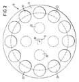
- Both the inclined surfaces 18 and the parabolic mirror 20 are each symmetrical about a forming the central axis of the light guide plate 10 Axis 32 arranged around distributed.
- the areas of the reflective layer 16 between the reflective Individual areas 18, 20 are not subject to any special measures Form areas as reflective surfaces. In principle it is possible, these intermediate areas, for example, by metallizing to mirror them as effective reflective surfaces for incident To use light.
- the reflecting individual surfaces 18 are each dependent on the Refractive index of the light guide plate 10 or the refractive index curve in the light guide plate 10 aligned so that through the light entry surface 14 in the light guide plate 10 incident light after reflection on the reflective Individual surfaces 18 on the light entry surface 14 of the total reflection is subjected and is forwarded to the receiving unit 12.
- reflective areas 36 are present, for example are produced by mirroring and in Fig. 1 only schematically are indicated. So that the reflective areas 36 the incidence do not interfere with light on the parabolic mirrors 20 are the parabolic mirrors 20 arranged as close as possible to the respective lens 22.
- the light rays 34 'of total reflection reflected by the parabolic mirrors be subjected to the light entry surface 14.
- the incident through the light entry surface 14 and in the light guide plate 10 propagating light is from the lens 15 of the receiving unit 12 collected and directed onto the light-sensitive surface of the photodiode 13, connected to a processing unit, not shown is.
- incident light beams are distributed over the light entry surface 14 one punctiform in comparison to the size of the light entry surface 14 Position can be summarized or concentrated.
- the light guide plate 10 in the case of the provision of a light emitting unit instead of the Light receiving unit 12 - the light guide plate 10 according to the invention able to initially present concentrated or bundled light beams after propagation and reflection in the light guide plate 10 via the as The opposite flat side serving the light exit surface is to be radiated in a distributed manner.
- the light guide plate 10 has a spatially constant refractive index. At least in principle, however, the light guide plate 10 could alternatively also can be provided with an arbitrary refractive index curve that with the design and arrangement of the reflective individual surfaces 18, 20 is coordinated and for example by targeted doping or by ion exchange when using special glasses can.
- the light entry surface 14 is the circular light guide plate 10 each formed as a lens 22 Subaperturen provided their centers on one by the dashed Line indicated circle around a by the receiving / transmitting unit 12 extending axis 32 of the light guide plate 10 and are even are distributed.
- the outer contour of the light guide plate 10 can in principle be chosen arbitrarily and is based on the geometry of the respective sensor or in general adapted to the overall arrangement.
- parabolic mirrors 20 in FIG. 2 are designed as parabolic mirrors 20 in FIG. 2 by way of example Concave mirror shown that part of the reflective surface 16 of the Form light guide plate 10 and with which according to the basis of Fig. 1 illustrated embodiment through the light entry surface 14 incident Light is thrown back onto the light entry surface 14 can.
- the parabolic mirrors 20 also lie on a circle around the axis 32 and are thus arranged concentrically with the lenses 22. After reflection on the light entry surface 14, which for this purpose on the corresponding Areas where there is no total reflection, for example is made reflective by metallizing, the light reaches the receiving unit arranged in the center of the lenses 22 or mirror 20 12th
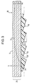
- Fig. 3 is partially a layered light guide plate 10th shown, together with a transmission and / or not shown Receiving unit forms an optical system according to the invention.
- the light guide plate 10 comprises a stack of individual plates 26 and one Reflection plate 24.
- the individual plates 26 are made of silicon (not in visible light), glass or plastic and for example by cementing together as well as with the injection molding process made of plastic reflection plate 24 connected.
- the reflection plate 24 is in principle in accordance with the embodiment of FIG Fig. 1 trained, wedge-shaped recesses 28 to form reflecting extending obliquely to the plane of the light guide plate 10 Individual surfaces 18 which together make up the majority of the Form reflection surface 16 of the light guide plate 10 and preferably by Metallizing are mirrored.
- the recesses 28 and thus the inclined surfaces 18 are over the entire Flat side of the light guide plate 10 distributed and such dimensioned to form a microstructure.
- the individual plates 26 are provided with different refractive indices n 1 to n 4 , increasing from the light entry surface 14 to the reflection surface 16, n 4 being mine than the refractive index n 5 of the reflection layer 24.
- This structure of the light guide plate 10 enables with a corresponding inclination angle ⁇ of the inclined surfaces 18, each in the example of FIG. 3 18 °, the generation of the light beam 34 in FIG. 3 exemplary beam path shown by repeated light refraction the interfaces between the individual plates 26 or layers.
- the light at the light entry surface 14 is subjected to total reflection, so that it is reflected back into the light guide plate 10 and so can be directed to a receiving unit, not shown.
- the Double arrow on the light beam 34 indicates that one in the reverse Direction of light propagation is possible.
- the reflection plate can be used 24 also connected a single plate, for example made of glass be, the refractive index like a grin lens continuously in the direction the reflection surface 16 increases.
- a refractive index curve can for example by targeted doping of the single plate or through ion exchange when using special glasses for the only one Plate can be reached.
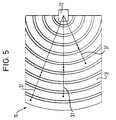
- Fig. 4 shows a also in layers of several individual plates 26 and a reflection plate 24 constructed light guide plate 10.
- the separating layer 27 At least in principle can also be used as the separating layer 27 a vacuum layer or at least a single plate with one for the The purpose of the separating layer 27, which has a suitable refractive index, is explained below be provided.
- the separating layer 27 is used from different angular ranges on the light entry surface 14 - and thus after reflection on an inclined surface 18 of the reflection surface 16 on the interface 27a between one Single plate 26 and the separating layer 27 - incident light rays 35, 35 'to separate, the arrows in Fig. 4 with different designs are provided.
- the refractive indices of the individual plates 26 are such chosen that originating from a first angular range, in Fig. 4 by a ray 35 represents light rays at the interface 27a of FIG Are subjected to total reflection, and that from a second angular range originating light rays represented in FIG.
- the incident light beams 35, 35 'thus as a function of their angle of incidence on the light guide plate 10 spreading in itself above and below the separating layer 27 Light separated.
- the limit angle of incidence from which to incident light rays at the boundary layer 27a totally reflected or broken, is particularly the number and design the individual plates 26 and depending on the separating layer 27 and can thus be specifically adjusted according to the invention.
- the light beams 35, 35 ' can be spatially separated Areas of a light-sensitive surface of a not shown Receiving unit can be detected that z. B. vertical to the level of the light guide plate 10 in the area of a light exit surface serving edge of the light guide plate 10 extends. It is also possible, to form the edge of the light guide plate 10 as a deflecting mirror, which the Beams of light 35, 35 'z. B. in the direction of in this case in the concerned Deflects the area serving as the light exit surface 16, and by means of a receiving unit arranged in this area to be proven spatially separate.
- the reverse light path is also possible, as in Fig. 4 is indicated by the double arrows.
- the inclined surfaces 18 z. B. each semicircular formed, with all inclined surfaces 18 the same angle of inclination ⁇ can have light rays 37, which are located at different distances from the unit 12 Inclined surfaces 18 are reflected, to be demonstrated in areas of the unit 12, that are perpendicular to the plane of the light guide plate 10 spatially apart are separated.
- the embodiments described above with reference to FIGS. 3 to 5 of the optical system according to the invention allow taking advantage the dispersion due to its layer structure and the associated repeated light refraction also a spectral decomposition of the incident light. For example, red and blue parts of the incident After reflection on the inclined surfaces 18 and refraction the first interface between the reflection plate 24 and the adjacent one Single plate 26 and all other interfaces different badly broken. Components of the wavelength having different wavelengths incident light thus spread in different areas of the Light guide plate 10 and can - z. B. according to the basis of Fig. 4 explained principle - on spatially separate areas of a receiving unit 12 can be demonstrated.
- the Lenses 22 can also be arranged inclined so that their optical axes run obliquely to the plane of the light guide plate 10.
- the tendencies of the Sloping surfaces 18 and the parabolic mirror 20 can also be larger or larger can be chosen smaller than in the mentioned embodiments.
- the inclined surfaces 18 and the parabolic mirrors 20 can also each further have different inclinations among each other.
- the light guide plate can also be made in another casting process be manufactured as an injection molding process.
- the structures on the flat sides of the light guide plate, especially the microstructures, can also after the production of a blank e.g. B. in an embossing, etching, doping and / or ion exchange process be formed.
- the surfaces can be used as filters, e.g. B. polarization or spectral filters, Aperture, beam splitter and / or beamformer are formed by the Areas z. B. provided with appropriate layers, suitably doped or otherwise treated, e.g. B. with three-dimensional microstructures be provided.
- filters e.g. B. polarization or spectral filters, Aperture, beam splitter and / or beamformer are formed by the Areas z. B. provided with appropriate layers, suitably doped or otherwise treated, e.g. B. with three-dimensional microstructures be provided.
- the optical properties of the light guide plate can in this way even when using a homogeneous base material in the plane of Light guide plate can be varied. This allows a Spatial and / or spatial frequency filtering can be integrated.
- microstructures involved in sandwiching the light guide plate each at the intermediate or boundary layers between two individual plates can be provided in such a way that they are very different Perform functions and for example as an aperture, filter, Beam splitters and / or beam formers are used.
- the Transmitting or receiving unit also in the area of the edges or narrow sides the light guide plate can be arranged.
- the subapertures and reflective Areas can be carried out such that the Light emerges from the light guide plate via the narrow sides or into the Light guide plate occurs, or that the light on, for example, as a deflecting mirror serving, bevelled narrow sides on the reflection surface and a receiving unit coupled to it or into the light guide plate is reflected into it.
- the sub-apertures can be combined with a light entry and - Exit surface can be arranged such that the light guide plate either has an autocollimation function or a complete one Pupil division exists. Also a so-called quasi-autocollimation function is feasible, one for blasting as well subaperture for receiving light of only for receiving is surrounded by light-serving sub-apertures.
- the invention enables several light guide plates z. B. in a common level to form a unit, e.g. B. Generate light grids with any geometry.
Landscapes
- Physics & Mathematics (AREA)
- General Physics & Mathematics (AREA)
- Optics & Photonics (AREA)
- Life Sciences & Earth Sciences (AREA)
- General Life Sciences & Earth Sciences (AREA)
- Geophysics (AREA)
- Light Guides In General And Applications Therefor (AREA)
- Optical Couplings Of Light Guides (AREA)
- Burglar Alarm Systems (AREA)
- Glass Compositions (AREA)
- Gyroscopes (AREA)
- Optical Elements Other Than Lenses (AREA)
Applications Claiming Priority (2)
| Application Number | Priority Date | Filing Date | Title |
|---|---|---|---|
| DE19858769A DE19858769A1 (de) | 1998-12-18 | 1998-12-18 | Optisches System |
| DE19858769 | 1998-12-18 |
Publications (3)
| Publication Number | Publication Date |
|---|---|
| EP1010992A2 true EP1010992A2 (fr) | 2000-06-21 |
| EP1010992A3 EP1010992A3 (fr) | 2003-03-19 |
| EP1010992B1 EP1010992B1 (fr) | 2006-05-31 |
Family
ID=7891770
Family Applications (1)
| Application Number | Title | Priority Date | Filing Date |
|---|---|---|---|
| EP99122759A Expired - Lifetime EP1010992B1 (fr) | 1998-12-18 | 1999-11-16 | Système optique |
Country Status (3)
| Country | Link |
|---|---|
| EP (1) | EP1010992B1 (fr) |
| AT (1) | ATE328295T1 (fr) |
| DE (2) | DE19858769A1 (fr) |
Cited By (1)
| Publication number | Priority date | Publication date | Assignee | Title |
|---|---|---|---|---|
| EP1686398A1 (fr) * | 2005-01-31 | 2006-08-02 | Sick Ag | Capteur optoélectronique |
Families Citing this family (5)
| Publication number | Priority date | Publication date | Assignee | Title |
|---|---|---|---|---|
| DE102006053229B4 (de) * | 2006-11-11 | 2008-07-31 | Sick Ag | Optoelektronischer Sensor und Verfahren zur Erfassung von Objekten mit polarisiertem Licht |
| DE102008063080B4 (de) * | 2008-12-24 | 2011-05-26 | Pantron Instruments Gmbh | Lichtschranke |
| DE102018105607B4 (de) | 2018-03-12 | 2022-05-25 | Sick Ag | Optoelektronischer Sensor und Verfahren zum Erfassen von Objekten in einem Überwachungsbereich |
| DE102019124266A1 (de) * | 2019-09-10 | 2021-03-11 | Sick Ag | Optoelektronischer Sensor und Verfahren zum Erfassen von Objekten in einem Überwachungsbereich |
| DE102019124265B4 (de) | 2019-09-10 | 2023-08-10 | Sick Ag | Optoelektronischer Sensor und Verfahren zum Erfassen von Objekten in einem Überwachungsbereich |
Citations (6)
| Publication number | Priority date | Publication date | Assignee | Title |
|---|---|---|---|---|
| DE2550814A1 (de) * | 1975-11-12 | 1977-05-26 | Sick Optik Elektronik Erwin | Zeilentastvorrichtung fuer materialbahnen zur fehlstellenermittlung |
| US4254333A (en) * | 1978-05-31 | 1981-03-03 | Bergstroem Arne | Optoelectronic circuit element |
| DE3119498A1 (de) * | 1981-05-15 | 1982-12-02 | Messerschmitt Boelkow Blohm | Objektiv |
| WO1996010206A1 (fr) * | 1994-09-29 | 1996-04-04 | Helfgott & Karas, P.C. | Dispositif a lentille |
| DE19601955A1 (de) * | 1996-01-09 | 1997-07-10 | Siemens Ag | Optoelektronische Sendebaugruppe |
| US5793538A (en) * | 1995-06-06 | 1998-08-11 | Hughes Missile Systems Company | Solid catadioptric lens |
Family Cites Families (2)
| Publication number | Priority date | Publication date | Assignee | Title |
|---|---|---|---|---|
| DE4329914A1 (de) * | 1993-09-04 | 1995-03-09 | Willing Gmbh Dr Ing | Linearer Lichtleiter |
| DE19510559C1 (de) * | 1995-03-23 | 1996-07-25 | Bosch Gmbh Robert | Optische Sende- und Empfangsanordnung |
-
1998
- 1998-12-18 DE DE19858769A patent/DE19858769A1/de not_active Withdrawn
-
1999
- 1999-11-16 DE DE59913486T patent/DE59913486D1/de not_active Expired - Lifetime
- 1999-11-16 EP EP99122759A patent/EP1010992B1/fr not_active Expired - Lifetime
- 1999-11-16 AT AT99122759T patent/ATE328295T1/de not_active IP Right Cessation
Patent Citations (6)
| Publication number | Priority date | Publication date | Assignee | Title |
|---|---|---|---|---|
| DE2550814A1 (de) * | 1975-11-12 | 1977-05-26 | Sick Optik Elektronik Erwin | Zeilentastvorrichtung fuer materialbahnen zur fehlstellenermittlung |
| US4254333A (en) * | 1978-05-31 | 1981-03-03 | Bergstroem Arne | Optoelectronic circuit element |
| DE3119498A1 (de) * | 1981-05-15 | 1982-12-02 | Messerschmitt Boelkow Blohm | Objektiv |
| WO1996010206A1 (fr) * | 1994-09-29 | 1996-04-04 | Helfgott & Karas, P.C. | Dispositif a lentille |
| US5793538A (en) * | 1995-06-06 | 1998-08-11 | Hughes Missile Systems Company | Solid catadioptric lens |
| DE19601955A1 (de) * | 1996-01-09 | 1997-07-10 | Siemens Ag | Optoelektronische Sendebaugruppe |
Cited By (2)
| Publication number | Priority date | Publication date | Assignee | Title |
|---|---|---|---|---|
| EP1686398A1 (fr) * | 2005-01-31 | 2006-08-02 | Sick Ag | Capteur optoélectronique |
| US7463419B2 (en) | 2005-01-31 | 2008-12-09 | Sick Ag | Optoelectronic sensor |
Also Published As
| Publication number | Publication date |
|---|---|
| ATE328295T1 (de) | 2006-06-15 |
| DE59913486D1 (de) | 2006-07-06 |
| DE19858769A1 (de) | 2000-06-21 |
| EP1010992A3 (fr) | 2003-03-19 |
| EP1010992B1 (fr) | 2006-05-31 |
Similar Documents
| Publication | Publication Date | Title |
|---|---|---|
| EP1316165B1 (fr) | Modificateur optique et son procede de production | |
| EP0238977B1 (fr) | Module émission-réception pour un réseau de communication bidirectionnelle, particulièrement un RNIS à large bande | |
| DE102008020171B4 (de) | Optische Sensorvorrichtung | |
| DE19610881B4 (de) | Mikrosystembaustein | |
| EP2120025B1 (fr) | Dispositif de capteur optique destiné à la détection de lumière ambiante | |
| EP0631163B1 (fr) | Emetteur-récepteur optique bidirectionnel | |
| EP3740749A1 (fr) | Dispositif de de détection pour la détection de salissures | |
| DE3503203A1 (de) | Optischer multiplexer/demultiplexer | |
| DE102017213465A1 (de) | Lichtleiter-basiertes LiDAR-System | |
| DE3313708A1 (de) | Optisches element | |
| DE102014115822A1 (de) | Ein optischer Multiplexer und Demultiplexer sowie ein Verfahren zum Herstellen und Zusammenbauen des Multiplexers/Demultiplexers | |
| EP2502036B1 (fr) | Dispositif capteur optique pour la détection de lumière ambiante dans des véhicules à moteur | |
| EP0025188B1 (fr) | Arrangement optique pour un photodétecteur | |
| EP1010992B1 (fr) | Système optique | |
| EP3620829A1 (fr) | Grille lumineuse | |
| DE3502382A1 (de) | Anordnung zur strahlenteilung eines laserstrahles | |
| EP0807842A2 (fr) | Dispositif optique avec élément optique diffractif | |
| DE102005010557B4 (de) | Optischer Multiplexer/Demultiplexer | |
| EP3654086B1 (fr) | Grille lumineuse | |
| WO2010040726A1 (fr) | Multiplexeur/demultiplexeur compact | |
| DE102019124265B4 (de) | Optoelektronischer Sensor und Verfahren zum Erfassen von Objekten in einem Überwachungsbereich | |
| EP1315992A2 (fr) | Dispositif de couplage et son procede de fabrication | |
| DE102022114792B3 (de) | Lichtsenderanordnung und optoelektronische sensoranordnung | |
| DE102017204550A1 (de) | Senderoptik für ein LiDAR-System, LiDAR-System und Arbeitsvorrichtung | |
| EP2044476A2 (fr) | Unité de filtre optique avec compensation |
Legal Events
| Date | Code | Title | Description |
|---|---|---|---|
| PUAI | Public reference made under article 153(3) epc to a published international application that has entered the european phase |
Free format text: ORIGINAL CODE: 0009012 |
|
| AK | Designated contracting states |
Kind code of ref document: A2 Designated state(s): AT BE CH CY DE DK ES FI FR GB GR IE IT LI LU MC NL PT SE |
|
| AX | Request for extension of the european patent |
Free format text: AL;LT;LV;MK;RO;SI |
|
| PUAL | Search report despatched |
Free format text: ORIGINAL CODE: 0009013 |
|
| AK | Designated contracting states |
Kind code of ref document: A3 Designated state(s): AT BE CH CY DE DK ES FI FR GB GR IE IT LI LU MC NL PT SE |
|
| AX | Request for extension of the european patent |
Extension state: AL LT LV MK RO SI |
|
| RIC1 | Information provided on ipc code assigned before grant |
Ipc: 7G 02B 17/08 B Ipc: 7G 01V 8/10 B Ipc: 7G 02B 5/00 B Ipc: 7G 01V 8/12 A |
|
| AKX | Designation fees paid | ||
| 17P | Request for examination filed |
Effective date: 20030509 |
|
| RBV | Designated contracting states (corrected) |
Designated state(s): AT BE CH CY DE DK ES FI FR GB GR IE IT LI LU MC NL PT SE |
|
| REG | Reference to a national code |
Ref country code: DE Ref legal event code: 8566 |
|
| 17Q | First examination report despatched |
Effective date: 20040527 |
|
| GRAP | Despatch of communication of intention to grant a patent |
Free format text: ORIGINAL CODE: EPIDOSNIGR1 |
|
| GRAS | Grant fee paid |
Free format text: ORIGINAL CODE: EPIDOSNIGR3 |
|
| GRAA | (expected) grant |
Free format text: ORIGINAL CODE: 0009210 |
|
| AK | Designated contracting states |
Kind code of ref document: B1 Designated state(s): AT BE CH CY DE DK ES FI FR GB GR IE IT LI LU MC NL PT SE |
|
| PG25 | Lapsed in a contracting state [announced via postgrant information from national office to epo] |
Ref country code: NL Free format text: LAPSE BECAUSE OF FAILURE TO SUBMIT A TRANSLATION OF THE DESCRIPTION OR TO PAY THE FEE WITHIN THE PRESCRIBED TIME-LIMIT Effective date: 20060531 Ref country code: IT Free format text: LAPSE BECAUSE OF FAILURE TO SUBMIT A TRANSLATION OF THE DESCRIPTION OR TO PAY THE FEE WITHIN THE PRESCRIBED TIME-LIMIT;WARNING: LAPSES OF ITALIAN PATENTS WITH EFFECTIVE DATE BEFORE 2007 MAY HAVE OCCURRED AT ANY TIME BEFORE 2007. THE CORRECT EFFECTIVE DATE MAY BE DIFFERENT FROM THE ONE RECORDED. Effective date: 20060531 Ref country code: IE Free format text: LAPSE BECAUSE OF FAILURE TO SUBMIT A TRANSLATION OF THE DESCRIPTION OR TO PAY THE FEE WITHIN THE PRESCRIBED TIME-LIMIT Effective date: 20060531 Ref country code: GB Free format text: LAPSE BECAUSE OF FAILURE TO SUBMIT A TRANSLATION OF THE DESCRIPTION OR TO PAY THE FEE WITHIN THE PRESCRIBED TIME-LIMIT Effective date: 20060531 Ref country code: FI Free format text: LAPSE BECAUSE OF FAILURE TO SUBMIT A TRANSLATION OF THE DESCRIPTION OR TO PAY THE FEE WITHIN THE PRESCRIBED TIME-LIMIT Effective date: 20060531 |
|
| REG | Reference to a national code |
Ref country code: GB Ref legal event code: FG4D Free format text: NOT ENGLISH Ref country code: CH Ref legal event code: EP |
|
| REG | Reference to a national code |
Ref country code: IE Ref legal event code: FG4D Free format text: LANGUAGE OF EP DOCUMENT: GERMAN |
|
| REF | Corresponds to: |
Ref document number: 59913486 Country of ref document: DE Date of ref document: 20060706 Kind code of ref document: P |
|
| PG25 | Lapsed in a contracting state [announced via postgrant information from national office to epo] |
Ref country code: SE Free format text: LAPSE BECAUSE OF FAILURE TO SUBMIT A TRANSLATION OF THE DESCRIPTION OR TO PAY THE FEE WITHIN THE PRESCRIBED TIME-LIMIT Effective date: 20060831 Ref country code: DK Free format text: LAPSE BECAUSE OF FAILURE TO SUBMIT A TRANSLATION OF THE DESCRIPTION OR TO PAY THE FEE WITHIN THE PRESCRIBED TIME-LIMIT Effective date: 20060831 |
|
| PG25 | Lapsed in a contracting state [announced via postgrant information from national office to epo] |
Ref country code: ES Free format text: LAPSE BECAUSE OF FAILURE TO SUBMIT A TRANSLATION OF THE DESCRIPTION OR TO PAY THE FEE WITHIN THE PRESCRIBED TIME-LIMIT Effective date: 20060911 |
|
| PG25 | Lapsed in a contracting state [announced via postgrant information from national office to epo] |
Ref country code: PT Free format text: LAPSE BECAUSE OF FAILURE TO SUBMIT A TRANSLATION OF THE DESCRIPTION OR TO PAY THE FEE WITHIN THE PRESCRIBED TIME-LIMIT Effective date: 20061031 |
|
| NLV1 | Nl: lapsed or annulled due to failure to fulfill the requirements of art. 29p and 29m of the patents act | ||
| PG25 | Lapsed in a contracting state [announced via postgrant information from national office to epo] |
Ref country code: MC Free format text: LAPSE BECAUSE OF NON-PAYMENT OF DUE FEES Effective date: 20061130 Ref country code: BE Free format text: LAPSE BECAUSE OF NON-PAYMENT OF DUE FEES Effective date: 20061130 |
|
| GBV | Gb: ep patent (uk) treated as always having been void in accordance with gb section 77(7)/1977 [no translation filed] |
Effective date: 20060531 |
|
| ET | Fr: translation filed | ||
| RAP2 | Party data changed (patent owner data changed or rights of a patent transferred) |
Owner name: SICK AG |
|
| PLBE | No opposition filed within time limit |
Free format text: ORIGINAL CODE: 0009261 |
|
| STAA | Information on the status of an ep patent application or granted ep patent |
Free format text: STATUS: NO OPPOSITION FILED WITHIN TIME LIMIT |
|
| 26N | No opposition filed |
Effective date: 20070301 |
|
| BERE | Be: lapsed |
Owner name: SICK A.G. Effective date: 20061130 |
|
| PG25 | Lapsed in a contracting state [announced via postgrant information from national office to epo] |
Ref country code: AT Free format text: LAPSE BECAUSE OF NON-PAYMENT OF DUE FEES Effective date: 20061116 |
|
| PG25 | Lapsed in a contracting state [announced via postgrant information from national office to epo] |
Ref country code: GR Free format text: LAPSE BECAUSE OF FAILURE TO SUBMIT A TRANSLATION OF THE DESCRIPTION OR TO PAY THE FEE WITHIN THE PRESCRIBED TIME-LIMIT Effective date: 20060901 |
|
| PG25 | Lapsed in a contracting state [announced via postgrant information from national office to epo] |
Ref country code: LU Free format text: LAPSE BECAUSE OF NON-PAYMENT OF DUE FEES Effective date: 20061116 |
|
| PG25 | Lapsed in a contracting state [announced via postgrant information from national office to epo] |
Ref country code: CY Free format text: LAPSE BECAUSE OF FAILURE TO SUBMIT A TRANSLATION OF THE DESCRIPTION OR TO PAY THE FEE WITHIN THE PRESCRIBED TIME-LIMIT Effective date: 20060531 |
|
| PGFP | Annual fee paid to national office [announced via postgrant information from national office to epo] |
Ref country code: IT Payment date: 20101126 Year of fee payment: 12 |
|
| PGFP | Annual fee paid to national office [announced via postgrant information from national office to epo] |
Ref country code: CH Payment date: 20111124 Year of fee payment: 13 Ref country code: FR Payment date: 20111125 Year of fee payment: 13 |
|
| REG | Reference to a national code |
Ref country code: CH Ref legal event code: PL |
|
| PG25 | Lapsed in a contracting state [announced via postgrant information from national office to epo] |
Ref country code: CH Free format text: LAPSE BECAUSE OF NON-PAYMENT OF DUE FEES Effective date: 20121130 Ref country code: LI Free format text: LAPSE BECAUSE OF NON-PAYMENT OF DUE FEES Effective date: 20121130 |
|
| REG | Reference to a national code |
Ref country code: FR Ref legal event code: ST Effective date: 20130731 |
|
| PG25 | Lapsed in a contracting state [announced via postgrant information from national office to epo] |
Ref country code: IT Free format text: LAPSE BECAUSE OF NON-PAYMENT OF DUE FEES Effective date: 20121116 |
|
| PG25 | Lapsed in a contracting state [announced via postgrant information from national office to epo] |
Ref country code: FR Free format text: LAPSE BECAUSE OF NON-PAYMENT OF DUE FEES Effective date: 20121130 |
|
| PGFP | Annual fee paid to national office [announced via postgrant information from national office to epo] |
Ref country code: DE Payment date: 20141120 Year of fee payment: 16 |
|
| REG | Reference to a national code |
Ref country code: DE Ref legal event code: R119 Ref document number: 59913486 Country of ref document: DE |
|
| PG25 | Lapsed in a contracting state [announced via postgrant information from national office to epo] |
Ref country code: DE Free format text: LAPSE BECAUSE OF NON-PAYMENT OF DUE FEES Effective date: 20160601 |