EP1006576A1 - Semiconductor device - Google Patents
Semiconductor device Download PDFInfo
- Publication number
- EP1006576A1 EP1006576A1 EP99309158A EP99309158A EP1006576A1 EP 1006576 A1 EP1006576 A1 EP 1006576A1 EP 99309158 A EP99309158 A EP 99309158A EP 99309158 A EP99309158 A EP 99309158A EP 1006576 A1 EP1006576 A1 EP 1006576A1
- Authority
- EP
- European Patent Office
- Prior art keywords
- electrode pad
- layer
- interconnection
- semiconductor device
- electrode
- Prior art date
- Legal status (The legal status is an assumption and is not a legal conclusion. Google has not performed a legal analysis and makes no representation as to the accuracy of the status listed.)
- Granted
Links
Images
Classifications
-
- H—ELECTRICITY
- H10—SEMICONDUCTOR DEVICES; ELECTRIC SOLID-STATE DEVICES NOT OTHERWISE PROVIDED FOR
- H10W—GENERIC PACKAGES, INTERCONNECTIONS, CONNECTORS OR OTHER CONSTRUCTIONAL DETAILS OF DEVICES COVERED BY CLASS H10
- H10W72/00—Interconnections or connectors in packages
- H10W72/071—Connecting or disconnecting
-
- H—ELECTRICITY
- H10—SEMICONDUCTOR DEVICES; ELECTRIC SOLID-STATE DEVICES NOT OTHERWISE PROVIDED FOR
- H10W—GENERIC PACKAGES, INTERCONNECTIONS, CONNECTORS OR OTHER CONSTRUCTIONAL DETAILS OF DEVICES COVERED BY CLASS H10
- H10W72/00—Interconnections or connectors in packages
- H10W72/20—Bump connectors, e.g. solder bumps or copper pillars; Dummy bumps; Thermal bumps
-
- H—ELECTRICITY
- H10—SEMICONDUCTOR DEVICES; ELECTRIC SOLID-STATE DEVICES NOT OTHERWISE PROVIDED FOR
- H10W—GENERIC PACKAGES, INTERCONNECTIONS, CONNECTORS OR OTHER CONSTRUCTIONAL DETAILS OF DEVICES COVERED BY CLASS H10
- H10W20/00—Interconnections in chips, wafers or substrates
- H10W20/40—Interconnections external to wafers or substrates, e.g. back-end-of-line [BEOL] metallisations or vias connecting to gate electrodes
-
- H—ELECTRICITY
- H10—SEMICONDUCTOR DEVICES; ELECTRIC SOLID-STATE DEVICES NOT OTHERWISE PROVIDED FOR
- H10W—GENERIC PACKAGES, INTERCONNECTIONS, CONNECTORS OR OTHER CONSTRUCTIONAL DETAILS OF DEVICES COVERED BY CLASS H10
- H10W72/00—Interconnections or connectors in packages
- H10W72/071—Connecting or disconnecting
- H10W72/075—Connecting or disconnecting of bond wires
- H10W72/07531—Techniques
- H10W72/07532—Compression bonding, e.g. thermocompression bonding
-
- H—ELECTRICITY
- H10—SEMICONDUCTOR DEVICES; ELECTRIC SOLID-STATE DEVICES NOT OTHERWISE PROVIDED FOR
- H10W—GENERIC PACKAGES, INTERCONNECTIONS, CONNECTORS OR OTHER CONSTRUCTIONAL DETAILS OF DEVICES COVERED BY CLASS H10
- H10W72/00—Interconnections or connectors in packages
- H10W72/20—Bump connectors, e.g. solder bumps or copper pillars; Dummy bumps; Thermal bumps
- H10W72/251—Materials
-
- H—ELECTRICITY
- H10—SEMICONDUCTOR DEVICES; ELECTRIC SOLID-STATE DEVICES NOT OTHERWISE PROVIDED FOR
- H10W—GENERIC PACKAGES, INTERCONNECTIONS, CONNECTORS OR OTHER CONSTRUCTIONAL DETAILS OF DEVICES COVERED BY CLASS H10
- H10W72/00—Interconnections or connectors in packages
- H10W72/20—Bump connectors, e.g. solder bumps or copper pillars; Dummy bumps; Thermal bumps
- H10W72/29—Bond pads specially adapted therefor
-
- H—ELECTRICITY
- H10—SEMICONDUCTOR DEVICES; ELECTRIC SOLID-STATE DEVICES NOT OTHERWISE PROVIDED FOR
- H10W—GENERIC PACKAGES, INTERCONNECTIONS, CONNECTORS OR OTHER CONSTRUCTIONAL DETAILS OF DEVICES COVERED BY CLASS H10
- H10W72/00—Interconnections or connectors in packages
- H10W72/50—Bond wires
- H10W72/531—Shapes of wire connectors
- H10W72/536—Shapes of wire connectors the connected ends being ball-shaped
-
- H—ELECTRICITY
- H10—SEMICONDUCTOR DEVICES; ELECTRIC SOLID-STATE DEVICES NOT OTHERWISE PROVIDED FOR
- H10W—GENERIC PACKAGES, INTERCONNECTIONS, CONNECTORS OR OTHER CONSTRUCTIONAL DETAILS OF DEVICES COVERED BY CLASS H10
- H10W72/00—Interconnections or connectors in packages
- H10W72/50—Bond wires
- H10W72/531—Shapes of wire connectors
- H10W72/5363—Shapes of wire connectors the connected ends being wedge-shaped
-
- H—ELECTRICITY
- H10—SEMICONDUCTOR DEVICES; ELECTRIC SOLID-STATE DEVICES NOT OTHERWISE PROVIDED FOR
- H10W—GENERIC PACKAGES, INTERCONNECTIONS, CONNECTORS OR OTHER CONSTRUCTIONAL DETAILS OF DEVICES COVERED BY CLASS H10
- H10W72/00—Interconnections or connectors in packages
- H10W72/50—Bond wires
- H10W72/59—Bond pads specially adapted therefor
-
- H—ELECTRICITY
- H10—SEMICONDUCTOR DEVICES; ELECTRIC SOLID-STATE DEVICES NOT OTHERWISE PROVIDED FOR
- H10W—GENERIC PACKAGES, INTERCONNECTIONS, CONNECTORS OR OTHER CONSTRUCTIONAL DETAILS OF DEVICES COVERED BY CLASS H10
- H10W72/00—Interconnections or connectors in packages
- H10W72/90—Bond pads, in general
-
- H—ELECTRICITY
- H10—SEMICONDUCTOR DEVICES; ELECTRIC SOLID-STATE DEVICES NOT OTHERWISE PROVIDED FOR
- H10W—GENERIC PACKAGES, INTERCONNECTIONS, CONNECTORS OR OTHER CONSTRUCTIONAL DETAILS OF DEVICES COVERED BY CLASS H10
- H10W72/00—Interconnections or connectors in packages
- H10W72/90—Bond pads, in general
- H10W72/931—Shapes of bond pads
- H10W72/934—Cross-sectional shape, i.e. in side view
-
- H—ELECTRICITY
- H10—SEMICONDUCTOR DEVICES; ELECTRIC SOLID-STATE DEVICES NOT OTHERWISE PROVIDED FOR
- H10W—GENERIC PACKAGES, INTERCONNECTIONS, CONNECTORS OR OTHER CONSTRUCTIONAL DETAILS OF DEVICES COVERED BY CLASS H10
- H10W72/00—Interconnections or connectors in packages
- H10W72/90—Bond pads, in general
- H10W72/951—Materials of bond pads
- H10W72/952—Materials of bond pads comprising metals or metalloids, e.g. PbSn, Ag or Cu
Definitions
- the present invention relates to semiconductor device, and particularly a semiconductor device of an area pad type.
- Chips of an area pad type are now becoming practically available.
- an electrode pad is formed on an interconnection or an active element for eliminating a region which is occupied only by the electrode pad, and thereby chip sizes are reduced.
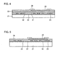
- an electrode pad portion of this semiconductor chip is provided with an insulating film 22, a first level interconnection also serving as an active element 23, an interlayer insulating film 24, an electrode pad 25 and a protective film 26 having an opening, which are formed in this order on semiconductor substrate 21.
- an interconnection and an active element 23 are formed immediately under electrode pad 25 with an interlayer insulating film 24 therebetween. Therefore, interconnection and active element 23 may be damaged and/or interlayer insulating film 24 may be cracked during wire bonding.
- the Japanese Patent Laying-Open No. 1-91439 disclosed an interlayer insulating film, which is made of three layers, which are formed of a plasma nitride film 31, a phase growth oxide film 32 and a vapor growth oxide film 33 containing impurity. This provides a structure having a good coverage and a large strength enough to withstand wire bonding.
- a plasma nitride film 31 a phase growth oxide film 32 and a vapor growth oxide film 33 containing impurity.
- a reference number 21 indicates a semiconductor substrate
- 22 indicates an oxide film
- 23 indicates an interconnection and active element
- 24 indicates an interlayer insulating film
- 25 indicates an electrode pad
- 26 indicates a protective film
- 31 indicates a plasma nitride film
- 32 indicates a vapor growth oxide film
- 33 indicates a vapor growth oxide film containing impurity
- 34 indicates an insulating film having a high adhesion to the electrode pad.
- a portion under the electrode pad may be damaged when bonding the tape carrier to an inner lead, and the pad may be peeled off.
- the quality of the finished interlayer film cannot be controlled without difficulty.
- a semiconductor device includes an interconnection or active element formed on a substrate, and an electrode pad formed on the interconnection or active element with an interlayer insulating film therebetween, and is provided with a projecting electrode formed on the surface of the electrode pad for protecting the interconnection or active element during bonding to an external terminal.
- the projecting electrode is preferably formed of at least one kind of material selected from a group consisting of Ni, Cu, Cu alloy and Ni alloy.
- the projecting electrode has a surface film made of at least one kind of material selected from a group consisting of Au, Pt and Ag.
- the projecting electrode is formed only in a formation region of the electrode pad.
- the projecting electrode has a height ranging from 0.5 ⁇ m to 10 ⁇ m.
- the surface film has a thickness ranging from 0.05 ⁇ m to 2 ⁇ m.
- the projecting electrode may be formed of an NiP layer having a phosphorus content of 7% to 11%.
- a semiconductor device includes a substrate, an active element, an electrode pad, an impact relieving layer and an external interconnection.
- the interconnection or active element is formed on the substrate.
- the electrode pad is formed on the interconnection or active element with an interlayer insulating film therebetween.
- the impact relieving layer is formed on the electrode pad for relieving an impact during bonding to an underlying portion of the electrode pad.
- the external interconnection is joined to the impact relieving layer by the bonding.
- the semiconductor device is provided with a protective film extending from a position above the interlayer insulating film to a position above a periphery of the electrode pad, and having an opening on the electrode pad.
- the impact relieving layer extends from a position above the electrode pad located in the opening to a position above the protective film.
- the external interconnection preferably includes a bonding wire or lead.
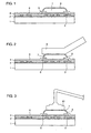
- Fig. 1 is a cross section showing a sectional structure of a pad of a semiconductor chip according to the invention.
- a reference number 1 indicates a semiconductor substrate
- 2 indicates an oxide film
- 3 indicates an interconnection and active element
- 4 indicates an interlayer insulating film
- 5 indicates an electrode pad
- 6 indicates a protective film
- 7 indicates an NiP layer (projecting electrode)
- 8 indicates an Au layer (surface layer).
- insulating layer 2, first-level interconnection and active layer 3, interlayer insulating film 4, electrode pad 5 and protective film 6 having an opening are formed in this order on semiconductor substrate 1.
- NiP layer 7 which contains 7% to 11% phosphorus and forms the projecting electrode of 5 ⁇ m in height as well as Au layer 8 which is 1 ⁇ m in thickness and forms a surface film for protecting the surface of the projecting electrode are formed in this order in the opening.
- NiP layer 7 and Au layer 8 are formed by electroless plating. For withstanding impacts during wire bonding and inner lead bonding, NiP layer 7 must have a height of 0.5 ⁇ m or more.
- the height of NiP layer 7 is preferably 10 ⁇ m or less in view of reduction of a time required for forming NiP layer 7.
- a similar effect can be achieved by a layer which is made of a material selected from a group including Ni, Cu, Ni alloy and Cu alloy.
- Au layer 8 is merely required to have a thickness of 0.05 ⁇ m or more. Even in the case where it is to be used for eutectic bonding with Sn, Au layer 8 is merely required to have a thickness of 2 ⁇ m or more. For reduction of the time required for forming Au layer 8, Au layer 8 preferably has a thickness in a range from 0.05 ⁇ m to 2 ⁇ m.
- the layer may be made of a noble metal such as Pt or Ag, or may be formed of a composite layer containing the noble metal, in which case a similar effect can be achieved.
- NiP layer 7 and Au layer 8 A method of forming NiP layer 7 and Au layer 8 will now be described.
- NiP layer 7 having a thickness of 5 ⁇ m measured from protective film 6. Deposition of NiP by this electroless plating has a selectivity.
- Ni layer is formed by a replacement reaction, which occurs between Ni and the Zn layer formed on the surface of electrode pad 5. Then, electroless plating progresses on the surface of the Ni layer owing to the autocatalysis. Accordingly, it is not necessary to form a resist pattern for plating. Further, it is not necessary to form a conductive film for plating on the wafer surface owing to the electroless plating.
- the electroless Ni plating solution used for the above is a general solution which is primarily made of nickel sulfate and sodium hypophosphite.
- Au layer 8 is formed on NiP layer 7.
- Ni on the surface of NiP layer 7 is replaced with Au using a substitution Au plating solution.
- This reaction is a replacement reaction, and Au layer 8 which is formed by this reaction can have a thickness of 0.1 ⁇ m or less. This thickness is large enough to protect the surface of NiP layer 7 by Au layer 8.
- electroless Au plating is further performed to increase the thickness of Au layer 8 to 1 ⁇ m.
- the electroless Au plating solution is primarily made of Au sodium sulfite.
- NiP layer 7 covers the opening of protective film 6, and does not have a portion protruding from a region where electrode pad 5 is formed.
- NiP layer 7 protected by Au layer 8 covers the protection opening, and serves to protect electrode pad 5 from corrosion and others. Owing to the structure where NiP layer 7 does not protrude from electrode pad 5, a stress can be relieved so that peeling of the pad and scooping of the underlying semiconductor substrate can be prevented.
- Fig. 2 is a cross section of the semiconductor chip of the TCP.
- insulating layer 2 In the semiconductor chip, insulating layer 2, first-level interconnection and active layer 3, interlayer insulating film 4, electrode pad 5 and protective film 6 having an opening are formed in this order on semiconductor substrate 1.
- NiP layer 7 containing 7% to 11% phosphorus as well as Au layer 8 are formed in this order in the opening.
- a tape carrier (not shown) has an insulating film having a device hole, and a conductor pattern is adhered onto this insulating film by adhesive. A conductor pattern which is integral with the foregoing conductor pattern is extended into the device hole, and a conductor lead 9 is coated with Sn plating.
- the bonding between the semiconductor chip and the tape carrier is achieved by Au-Sn eutectic crystal, which is formed by thermo compression bonding between Au layer 8 on electrode pad 5 and the Sn layer of conductor lead 9.
- Fig. 3 is a cross section of the semiconductor chip according to the invention, which is housed in a plastic mold package and is mounted on a substrate (printed board or ceramic board: not shown). Even in the structure where a wire 10 is bonded onto projecting electrode 7 as shown in Fig. 3, damages which may be caused to electrode pad 5 and the underlying portion by the wire bonding can be prevented, similarly to the case of the TCP.
- the description has been given on the example in which the hard projecting electrode is formed of Ni-contained metal. Instead of this, Cu-contained metal may be used as a hard material of the projecting electrode which can be formed of electroless plating.
- the projecting electrode relieves the impact which may occur during wire bonding or inner lead bonding, even when the wire bonding or inner lead bonding is performed on the electrode pad. Therefore, no damage is caused to the electrode pad as well as the interlayer insulating film, and the interconnection layer and active layer under the pad. Accordingly, it is possible to improve yield during assembly as well as reliability of connection. Since the hard projecting electrode is formed in the protective film opening on the electrode pad, it is possible to measure a shearing strength in a lateral direction and detect an adhesive strength so that adhesion can be determined before the assembly.
- the structure in the prior art is not provided with a projecting electrode, and therefore is not provided with a catch, hook or the like so that measurement is physically impossible in the prior art. By forming the projecting electrode, a tool of measuring the shearing strength or the like can be hooked on the projecting electrode, and thereby the measurement of the shearing strength can be performed.
- the surface film made of an Ag layer, Pt layer, Au layer or the like By forming the surface film made of an Ag layer, Pt layer, Au layer or the like on the surface of the projecting electrode, the surface oxidation of the projecting electrode can be prevented. Further, no problem arises even if it is used for eutectic bonding between the Au layer and Sn.
- the Cu layer, Ni layer, Cu alloy layer, Ni alloy layer, Ag layer, Pt layer and Au layer can be formed by electroless plating, complicated steps for electrolytic plating are not required.
- the projecting electrode By forming the projecting electrode in the electrode pad formation region, it is possible to prevent peeling of the electrode pad and scooping of the underlying semiconductor substrate, which may be caused by a stress applied from the projecting electrode.
Landscapes
- Wire Bonding (AREA)
- Internal Circuitry In Semiconductor Integrated Circuit Devices (AREA)
Abstract
Description
- The present invention relates to semiconductor device, and particularly a semiconductor device of an area pad type.
- Chips of an area pad type are now becoming practically available. In the area pad type, an electrode pad is formed on an interconnection or an active element for eliminating a region which is occupied only by the electrode pad, and thereby chip sizes are reduced. As shown in Fig. 5, an electrode pad portion of this semiconductor chip is provided with an
insulating film 22, a first level interconnection also serving as anactive element 23, an interlayerinsulating film 24, anelectrode pad 25 and aprotective film 26 having an opening, which are formed in this order onsemiconductor substrate 21. In this case, an interconnection and anactive element 23 are formed immediately underelectrode pad 25 with aninterlayer insulating film 24 therebetween. Therefore, interconnection andactive element 23 may be damaged and/or interlayer insulatingfilm 24 may be cracked during wire bonding. - In connection with the above problems, the Japanese Patent Laying-Open No. 1-91439 disclosed an interlayer insulating film, which is made of three layers, which are formed of a
plasma nitride film 31, a phasegrowth oxide film 32 and a vaporgrowth oxide film 33 containing impurity. This provides a structure having a good coverage and a large strength enough to withstand wire bonding. In Figs. 4 and 5, areference number 21 indicates a semiconductor substrate, 22 indicates an oxide film, 23 indicates an interconnection and active element, 24 indicates an interlayer insulating film, 25 indicates an electrode pad, 26 indicates a protective film, 31 indicates a plasma nitride film, 32 indicates a vapor growth oxide film, 33 indicates a vapor growth oxide film containing impurity, and 34 indicates an insulating film having a high adhesion to the electrode pad. - In a TCP (Tape Carrier Package) structure in which an Au bump is formed on an electrode pad, a portion under the electrode pad may be damaged when bonding the tape carrier to an inner lead, and the pad may be peeled off.
- Techniques relating to formation of an Ni bump on an electrode pad have been disclosed in Japanese Patent Laying-Open No. 8-264541 and others. However, this publication has not disclosed a structure, in which an interconnection or active element is arranged under an electrode pad with an interlayer insulating film therebetween.
- However, the foregoing countermeasures require a significant change in wafer manufacturing step, and complicate the manufacturing steps. For employing the above countermeasures in various kinds of devices, an interlayer film must be changed in every process. However, change to the interlayer film cannot be made without difficulty because it affects the quality and characteristics of the devices.
- If the pad is not provided with a projection, the quality of the finished interlayer film cannot be controlled without difficulty. For controlling the quality of the interlayer film, it is necessary to break the wafer for determining the section, resulting in increase in cost. It is also difficult to measure the adhesion between the interlayer film and the electrode pad. Accordingly, even when a certain trouble occurred due to insufficient adhesion between them, the problem cannot be found before performing actual assembly so that products including such troubles may be placed on the market, resulting in another problem.
- According to an aspect of the invention, a semiconductor device includes an interconnection or active element formed on a substrate, and an electrode pad formed on the interconnection or active element with an interlayer insulating film therebetween, and is provided with a projecting electrode formed on the surface of the electrode pad for protecting the interconnection or active element during bonding to an external terminal.
- The projecting electrode is preferably formed of at least one kind of material selected from a group consisting of Ni, Cu, Cu alloy and Ni alloy.
- Preferably, the projecting electrode has a surface film made of at least one kind of material selected from a group consisting of Au, Pt and Ag.
- The projecting electrode is formed only in a formation region of the electrode pad.
- The projecting electrode has a height ranging from 0.5 µm to 10 µm.
- The surface film has a thickness ranging from 0.05 µm to 2 µm.
- The projecting electrode may be formed of an NiP layer having a phosphorus content of 7% to 11%.
- According to another aspect of the invention, a semiconductor device includes a substrate, an active element, an electrode pad, an impact relieving layer and an external interconnection. The interconnection or active element is formed on the substrate. The electrode pad is formed on the interconnection or active element with an interlayer insulating film therebetween. The impact relieving layer is formed on the electrode pad for relieving an impact during bonding to an underlying portion of the electrode pad. The external interconnection is joined to the impact relieving layer by the bonding.
- The semiconductor device is provided with a protective film extending from a position above the interlayer insulating film to a position above a periphery of the electrode pad, and having an opening on the electrode pad. In this structure, the impact relieving layer extends from a position above the electrode pad located in the opening to a position above the protective film.
- The external interconnection preferably includes a bonding wire or lead.
- The foregoing and other objects, features, aspects and advantages of the present invention will become more apparent from the following detailed description of the present invention when taken in conjunction with the accompanying drawings.
-
- Fig. 1 is a cross section showing a sectional structure of a pad of a semiconductor chip according to the invention;
- Fig. 2 is a cross section showing the sectional structure of the pad of the semiconductor chip according to the invention together with a TCP attached thereto;
- Fig. 3 is a cross section showing the sectional structure of the pad of the semiconductor chip according to the invention together with a plastic mold package and a substrate (printed board or ceramic board);
- Fig. 4 is a cross section showing by way of example the pad structure of the semiconductor chip in the prior art; and
- Fig. 5 is a cross section showing another example of the pad structure of the semiconductor chip in the prior art.
-
- The invention will now be described in greater detail with reference to embodiments.
- Fig. 1 is a cross section showing a sectional structure of a pad of a semiconductor chip according to the invention. A
reference number 1 indicates a semiconductor substrate, 2 indicates an oxide film, 3 indicates an interconnection and active element, 4 indicates an interlayer insulating film, 5 indicates an electrode pad, 6 indicates a protective film, 7 indicates an NiP layer (projecting electrode) and 8 indicates an Au layer (surface layer). - As shown in Fig. 1,
insulating layer 2, first-level interconnection andactive layer 3, interlayerinsulating film 4,electrode pad 5 andprotective film 6 having an opening are formed in this order onsemiconductor substrate 1.NiP layer 7 which contains 7% to 11% phosphorus and forms the projecting electrode of 5 µm in height as well asAu layer 8 which is 1 µm in thickness and forms a surface film for protecting the surface of the projecting electrode are formed in this order in the opening.NiP layer 7 andAu layer 8 are formed by electroless plating. For withstanding impacts during wire bonding and inner lead bonding,NiP layer 7 must have a height of 0.5 µm or more. Also, the height ofNiP layer 7 is preferably 10 µm or less in view of reduction of a time required for formingNiP layer 7. Instead of the NiP layer, a similar effect can be achieved by a layer which is made of a material selected from a group including Ni, Cu, Ni alloy and Cu alloy. - For preventing surface oxidation of
NiP layer 7,Au layer 8 is merely required to have a thickness of 0.05 µm or more. Even in the case where it is to be used for eutectic bonding with Sn,Au layer 8 is merely required to have a thickness of 2 µm or more. For reduction of the time required for formingAu layer 8,Au layer 8 preferably has a thickness in a range from 0.05 µm to 2 µm. Instead ofAu layer 8, the layer may be made of a noble metal such as Pt or Ag, or may be formed of a composite layer containing the noble metal, in which case a similar effect can be achieved. - A method of forming
NiP layer 7 andAu layer 8 will now be described. - First, A1 on the surface of
electrode pad 5, which is exposed through the opening formed inprotective film 6, is replaced with Zn allowing a replacement (substitution) reaction with Ni. Then, the chip is immersed into a plating solution, and electroless plating is performed to formNiP layer 7 having a thickness of 5 µm measured fromprotective film 6. Deposition of NiP by this electroless plating has a selectivity. - An Ni layer is formed by a replacement reaction, which occurs between Ni and the Zn layer formed on the surface of
electrode pad 5. Then, electroless plating progresses on the surface of the Ni layer owing to the autocatalysis. Accordingly, it is not necessary to form a resist pattern for plating. Further, it is not necessary to form a conductive film for plating on the wafer surface owing to the electroless plating. - The electroless Ni plating solution used for the above is a general solution which is primarily made of nickel sulfate and sodium hypophosphite.
- Then,
Au layer 8 is formed onNiP layer 7. Ni on the surface ofNiP layer 7 is replaced with Au using a substitution Au plating solution. This reaction is a replacement reaction, andAu layer 8 which is formed by this reaction can have a thickness of 0.1 µm or less. This thickness is large enough to protect the surface ofNiP layer 7 byAu layer 8. - Further, electroless Au plating is further performed to increase the thickness of
Au layer 8 to 1 µm. The electroless Au plating solution is primarily made of Au sodium sulfite. - At this time,
NiP layer 7 covers the opening ofprotective film 6, and does not have a portion protruding from a region whereelectrode pad 5 is formed. Owing to this structure,NiP layer 7 protected byAu layer 8 covers the protection opening, and serves to protectelectrode pad 5 from corrosion and others. Owing to the structure whereNiP layer 7 does not protrude fromelectrode pad 5, a stress can be relieved so that peeling of the pad and scooping of the underlying semiconductor substrate can be prevented. - Since strengths of
electrode pad 5 and its underlying portion can be measured through NiP layer, the adhesion can be controlled. - Fig. 2 is a cross section of the semiconductor chip of the TCP. In the semiconductor chip, insulating
layer 2, first-level interconnection andactive layer 3,interlayer insulating film 4,electrode pad 5 andprotective film 6 having an opening are formed in this order onsemiconductor substrate 1.NiP layer 7 containing 7% to 11% phosphorus as well asAu layer 8 are formed in this order in the opening. - A tape carrier (not shown) has an insulating film having a device hole, and a conductor pattern is adhered onto this insulating film by adhesive. A conductor pattern which is integral with the foregoing conductor pattern is extended into the device hole, and a
conductor lead 9 is coated with Sn plating. - In the TCP described above, the bonding between the semiconductor chip and the tape carrier is achieved by Au-Sn eutectic crystal, which is formed by thermo compression bonding between
Au layer 8 onelectrode pad 5 and the Sn layer ofconductor lead 9. - After the thermo compression deposition,
conductor lead 9 and projectingelectrode 7 were removed, and the states ofelectrode pad 5 and its underlying portion were determined. Even under such conditions that the load was 50 gram-weight (0.49 newton) per electrode and the temperature was 560°C, no damage was caused. Under the same conditions, a projecting electrode made of only Au was determined. In this case, it was found that the electrode pad and the underlying portion were damaged. - Fig. 3 is a cross section of the semiconductor chip according to the invention, which is housed in a plastic mold package and is mounted on a substrate (printed board or ceramic board: not shown). Even in the structure where a
wire 10 is bonded onto projectingelectrode 7 as shown in Fig. 3, damages which may be caused toelectrode pad 5 and the underlying portion by the wire bonding can be prevented, similarly to the case of the TCP. The description has been given on the example in which the hard projecting electrode is formed of Ni-contained metal. Instead of this, Cu-contained metal may be used as a hard material of the projecting electrode which can be formed of electroless plating. - According to the invention, as described above, the projecting electrode relieves the impact which may occur during wire bonding or inner lead bonding, even when the wire bonding or inner lead bonding is performed on the electrode pad. Therefore, no damage is caused to the electrode pad as well as the interlayer insulating film, and the interconnection layer and active layer under the pad. Accordingly, it is possible to improve yield during assembly as well as reliability of connection. Since the hard projecting electrode is formed in the protective film opening on the electrode pad, it is possible to measure a shearing strength in a lateral direction and detect an adhesive strength so that adhesion can be determined before the assembly. The structure in the prior art is not provided with a projecting electrode, and therefore is not provided with a catch, hook or the like so that measurement is physically impossible in the prior art. By forming the projecting electrode, a tool of measuring the shearing strength or the like can be hooked on the projecting electrode, and thereby the measurement of the shearing strength can be performed.
- By forming the surface film made of an Ag layer, Pt layer, Au layer or the like on the surface of the projecting electrode, the surface oxidation of the projecting electrode can be prevented. Further, no problem arises even if it is used for eutectic bonding between the Au layer and Sn.
- Since the Cu layer, Ni layer, Cu alloy layer, Ni alloy layer, Ag layer, Pt layer and Au layer can be formed by electroless plating, complicated steps for electrolytic plating are not required.
- By forming the projecting electrode in the electrode pad formation region, it is possible to prevent peeling of the electrode pad and scooping of the underlying semiconductor substrate, which may be caused by a stress applied from the projecting electrode.
- Although the present invention has been described and illustrated in detail, it is clearly understood that the same is by way of illustration and example only and is not to be taken by way of limitation, the spirit and scope of the present invention being limited only by the terms of the appended claims.
Claims (10)
- A semiconductor device comprising an interconnection or active element (3) formed on a substrate (1), and an electrode pad (5) formed on said interconnection or active element (3) with an interlayer insulating film (4) therebetween, wherein
a projecting electrode (7) is formed on the surface of said electrode pad (5) for protecting said interconnection or active element (3) during bonding to an external terminal. - The semiconductor device according to claim 1, wherein
said projecting electrode (7) is formed of at least one kind of material selected from a group consisting of Ni, Cu, Cu alloy and Ni alloy. - The semiconductor device according to claim 1, wherein
said projecting electrode (7) has a surface film (8) made of at least one kind of material selected from a group consisting of Au, Pt and Ag. - The semiconductor device according to claim 1, wherein
said projecting electrode (7) is formed only in a formation region of said electrode pad (5). - The semiconductor device according to claim 1, wherein
said projecting electrode (7) has a height ranging from 0.5 µm to 10 µm. - The semiconductor device according to claim 1, wherein
said surface film (8) has a thickness ranging from 0.05 µm to 2 µm. - The semiconductor device according to claim 1, whereinsaid projecting electrode (7) is formed of an NiP layer, andsaid NiP layer has a phosphorus content of 7% to 11%.
- A semiconductor device comprising:a substrate (1);an interconnection or active element (3) formed on said substrate (1);an electrode pad (5) formed on said interconnection or active element (3) with an interlayer insulating film (4) therebetween;an impact relieving layer (7) formed on said electrode pad (5) for relieving an impact during bonding to an underlying portion of said electrode pad (5); andan external interconnection (9, 10) joined to said impact relieving layer (7) by the bonding.
- The semiconductor device according to claim 8, further comprising:a protective film (6) extending from a position above said interlayer insulating film (4) to a position above a periphery of said electrode pad (5), and having an opening on said electrode pad (5), whereinsaid impact relieving layer (7) extends from a position above said electrode pad (5) located in said opening to a position above said protective film (6).
- The semiconductor device according to claim 8, wherein
said external interconnection (9, 10) includes a bonding wire or lead.
Applications Claiming Priority (2)
| Application Number | Priority Date | Filing Date | Title |
|---|---|---|---|
| JP33863998 | 1998-11-30 | ||
| JP33863998A JP3398609B2 (en) | 1998-11-30 | 1998-11-30 | Semiconductor device |
Publications (2)
| Publication Number | Publication Date |
|---|---|
| EP1006576A1 true EP1006576A1 (en) | 2000-06-07 |
| EP1006576B1 EP1006576B1 (en) | 2003-11-05 |
Family
ID=18320076
Family Applications (1)
| Application Number | Title | Priority Date | Filing Date |
|---|---|---|---|
| EP99309158A Expired - Lifetime EP1006576B1 (en) | 1998-11-30 | 1999-11-17 | Semiconductor device |
Country Status (6)
| Country | Link |
|---|---|
| US (1) | US20020056901A1 (en) |
| EP (1) | EP1006576B1 (en) |
| JP (1) | JP3398609B2 (en) |
| KR (1) | KR100356770B1 (en) |
| DE (1) | DE69912565T2 (en) |
| TW (1) | TW440962B (en) |
Cited By (6)
| Publication number | Priority date | Publication date | Assignee | Title |
|---|---|---|---|---|
| EP1320129A1 (en) * | 2001-12-14 | 2003-06-18 | STMicroelectronics S.r.l. | Semiconductor electronic device and method of manufacturing thereof. |
| WO2004059722A1 (en) * | 2002-12-24 | 2004-07-15 | Denso Corporation | Semiconductor sensor and plating method for semiconductor device |
| WO2004105133A1 (en) * | 2003-05-26 | 2004-12-02 | Axalto Sa | Wire bonding on in-line connection pads |
| WO2008110216A1 (en) * | 2007-03-15 | 2008-09-18 | L'air Liquide Societe Anonyme Pour L'etude Et L'exploitation Des Procedes Georges Claude | Copper interconnection for flat panel display manufacturing |
| US7851913B2 (en) | 2006-11-06 | 2010-12-14 | Infineon Technologies Ag | Semiconductor device including a power device with first metal layer and second metal layer laterally spaced apart |
| EP3336889A1 (en) * | 2016-12-12 | 2018-06-20 | Infineon Technologies Austria AG | Semiconductor device, electronic component and method |
Families Citing this family (23)
| Publication number | Priority date | Publication date | Assignee | Title |
|---|---|---|---|---|
| JP3405697B2 (en) | 1999-09-20 | 2003-05-12 | ローム株式会社 | Semiconductor chip |
| KR100385165B1 (en) * | 2000-09-25 | 2003-05-22 | 삼성테크윈 주식회사 | Semiconductor package and the fabrication method of the same |
| JP3727272B2 (en) | 2002-01-15 | 2005-12-14 | 沖電気工業株式会社 | Semiconductor device and manufacturing method of semiconductor device |
| JP2003229517A (en) * | 2002-01-31 | 2003-08-15 | Fujitsu Hitachi Plasma Display Ltd | Semiconductor chip mounting board and flat display |
| KR20030094692A (en) * | 2002-06-07 | 2003-12-18 | 삼성테크윈 주식회사 | Method of forming electroless solder bumps |
| JP2005116632A (en) | 2003-10-03 | 2005-04-28 | Rohm Co Ltd | Semiconductor device manufacturing method and semiconductor device |
| JP4661122B2 (en) * | 2004-05-18 | 2011-03-30 | ソニー株式会社 | Component mounting wiring board and mounting method of components on wiring board |
| JP4604641B2 (en) * | 2004-10-18 | 2011-01-05 | 株式会社デンソー | Semiconductor device |
| DE102005028951B4 (en) | 2005-06-22 | 2018-05-30 | Infineon Technologies Ag | Arrangement for the electrical connection of a semiconductor circuit arrangement with an external contact device |
| DE102005033469B4 (en) | 2005-07-18 | 2019-05-09 | Infineon Technologies Ag | Method for producing a semiconductor module |
| JP2008124437A (en) | 2006-10-19 | 2008-05-29 | Matsushita Electric Ind Co Ltd | Semiconductor wafer, manufacturing method thereof, and manufacturing method of semiconductor chip |
| US8293587B2 (en) | 2007-10-11 | 2012-10-23 | International Business Machines Corporation | Multilayer pillar for reduced stress interconnect and method of making same |
| JP4806468B2 (en) * | 2008-02-29 | 2011-11-02 | 三洋電機株式会社 | Semiconductor module |
| JP4588091B2 (en) | 2008-02-29 | 2010-11-24 | 三洋電機株式会社 | Manufacturing method of semiconductor module |
| JP2009246218A (en) | 2008-03-31 | 2009-10-22 | Renesas Technology Corp | Semiconductor device and method for manufacturing the same |
| JP5331610B2 (en) | 2008-12-03 | 2013-10-30 | ルネサスエレクトロニクス株式会社 | Semiconductor integrated circuit device |
| JP2010141112A (en) * | 2008-12-11 | 2010-06-24 | Sharp Corp | Semiconductor device and method of manufacturing semiconductor device |
| US20120261812A1 (en) * | 2011-04-14 | 2012-10-18 | Topacio Roden R | Semiconductor chip with patterned underbump metallization |
| JP2012160739A (en) * | 2012-03-14 | 2012-08-23 | Renesas Electronics Corp | Semiconductor device |
| JP2013229491A (en) * | 2012-04-26 | 2013-11-07 | Kyocera Corp | Electrode structure, semiconductor element, semiconductor device, thermal head, and thermal printer |
| US9576923B2 (en) | 2014-04-01 | 2017-02-21 | Ati Technologies Ulc | Semiconductor chip with patterned underbump metallization and polymer film |
| JP2018186144A (en) | 2017-04-25 | 2018-11-22 | 株式会社村田製作所 | Semiconductor device and power amplifier module |
| DE102023205979A1 (en) | 2023-06-26 | 2025-01-02 | Robert Bosch Gesellschaft mit beschränkter Haftung | contact system with a contact carrier and a bonding wire |
Citations (4)
| Publication number | Priority date | Publication date | Assignee | Title |
|---|---|---|---|---|
| JPS528785A (en) * | 1975-07-10 | 1977-01-22 | Citizen Watch Co Ltd | Semiconductor device electrode structure |
| JPH0214527A (en) * | 1988-11-11 | 1990-01-18 | Seiko Epson Corp | Semiconductor device |
| JPH02296336A (en) * | 1989-05-10 | 1990-12-06 | Seiko Epson Corp | Manufacture of semiconductor circuit bump |
| EP0646959A1 (en) * | 1993-09-30 | 1995-04-05 | Consorzio per la Ricerca sulla Microelettronica nel Mezzogiorno - CoRiMMe | Metallization and bonding process for manufacturing power semiconductor devices |
-
1998
- 1998-11-30 JP JP33863998A patent/JP3398609B2/en not_active Expired - Lifetime
-
1999
- 1999-11-17 DE DE69912565T patent/DE69912565T2/en not_active Expired - Lifetime
- 1999-11-17 EP EP99309158A patent/EP1006576B1/en not_active Expired - Lifetime
- 1999-11-17 TW TW088120029A patent/TW440962B/en not_active IP Right Cessation
- 1999-11-26 KR KR1019990052984A patent/KR100356770B1/en not_active Expired - Fee Related
- 1999-11-29 US US09/449,864 patent/US20020056901A1/en not_active Abandoned
Patent Citations (4)
| Publication number | Priority date | Publication date | Assignee | Title |
|---|---|---|---|---|
| JPS528785A (en) * | 1975-07-10 | 1977-01-22 | Citizen Watch Co Ltd | Semiconductor device electrode structure |
| JPH0214527A (en) * | 1988-11-11 | 1990-01-18 | Seiko Epson Corp | Semiconductor device |
| JPH02296336A (en) * | 1989-05-10 | 1990-12-06 | Seiko Epson Corp | Manufacture of semiconductor circuit bump |
| EP0646959A1 (en) * | 1993-09-30 | 1995-04-05 | Consorzio per la Ricerca sulla Microelettronica nel Mezzogiorno - CoRiMMe | Metallization and bonding process for manufacturing power semiconductor devices |
Non-Patent Citations (3)
| Title |
|---|
| PATENT ABSTRACTS OF JAPAN vol. 001, no. 072 (E - 028) 13 July 1977 (1977-07-13) * |
| PATENT ABSTRACTS OF JAPAN vol. 014, no. 156 (E - 0908) 26 March 1990 (1990-03-26) * |
| PATENT ABSTRACTS OF JAPAN vol. 015, no. 078 (E - 1037) 22 February 1991 (1991-02-22) * |
Cited By (10)
| Publication number | Priority date | Publication date | Assignee | Title |
|---|---|---|---|---|
| EP1320129A1 (en) * | 2001-12-14 | 2003-06-18 | STMicroelectronics S.r.l. | Semiconductor electronic device and method of manufacturing thereof. |
| US6815789B2 (en) | 2001-12-14 | 2004-11-09 | Stmicroelectronics S.R.L. | Semiconductor electronic device and method of manufacturing thereof |
| US7459387B2 (en) | 2001-12-14 | 2008-12-02 | Stmicroelectronics S.R.L. | Semiconductor electronic device and method of manufacturing thereof |
| WO2004059722A1 (en) * | 2002-12-24 | 2004-07-15 | Denso Corporation | Semiconductor sensor and plating method for semiconductor device |
| CN101145532B (en) * | 2002-12-24 | 2010-06-02 | 株式会社电装 | Method for electroplating semiconductor devices |
| WO2004105133A1 (en) * | 2003-05-26 | 2004-12-02 | Axalto Sa | Wire bonding on in-line connection pads |
| US7851913B2 (en) | 2006-11-06 | 2010-12-14 | Infineon Technologies Ag | Semiconductor device including a power device with first metal layer and second metal layer laterally spaced apart |
| WO2008110216A1 (en) * | 2007-03-15 | 2008-09-18 | L'air Liquide Societe Anonyme Pour L'etude Et L'exploitation Des Procedes Georges Claude | Copper interconnection for flat panel display manufacturing |
| EP3336889A1 (en) * | 2016-12-12 | 2018-06-20 | Infineon Technologies Austria AG | Semiconductor device, electronic component and method |
| US11380612B2 (en) | 2016-12-12 | 2022-07-05 | Infineon Technologies Austria Ag | Semiconductor device, electronic component and method |
Also Published As
| Publication number | Publication date |
|---|---|
| KR20000035730A (en) | 2000-06-26 |
| EP1006576B1 (en) | 2003-11-05 |
| KR100356770B1 (en) | 2002-10-19 |
| TW440962B (en) | 2001-06-16 |
| US20020056901A1 (en) | 2002-05-16 |
| DE69912565T2 (en) | 2004-09-16 |
| JP2000164623A (en) | 2000-06-16 |
| DE69912565D1 (en) | 2003-12-11 |
| JP3398609B2 (en) | 2003-04-21 |
Similar Documents
| Publication | Publication Date | Title |
|---|---|---|
| EP1006576B1 (en) | Semiconductor device | |
| US6607941B2 (en) | Process and structure improvements to shellcase style packaging technology | |
| USRE46466E1 (en) | Method for fabricating low resistance, low inductance interconnections in high current semiconductor devices | |
| US7855103B2 (en) | Wirebond structure and method to connect to a microelectronic die | |
| EP1564810B1 (en) | Semiconductor device and manufacturing method thereof | |
| US5631499A (en) | Semiconductor device comprising fine bump electrode having small side etch portion and stable characteristics | |
| US7485967B2 (en) | Semiconductor device with via hole for electric connection | |
| US9385008B2 (en) | Semiconductor component of semiconductor chip size with flip-chip-like external contacts | |
| US5132772A (en) | Semiconductor device having tape automated bonding (TAB) leads which facilitate lead bonding | |
| EP1653509A2 (en) | Semiconductor device and manufacturing method of the same | |
| EP1653508A2 (en) | Semiconductor device and manufacturing method of the same | |
| EP1686622A2 (en) | Semiconductor device and manufacturing method of the same | |
| US20050242446A1 (en) | Integrated circuit package with different hardness bump pad and bump and manufacturing method therefor | |
| US20010013651A1 (en) | Semiconductor device and manufacturing method therefor | |
| US12374622B2 (en) | Semiconductor device with improved internal and external electrode structure | |
| JPH07201865A (en) | Semiconductor device with bumps | |
| CN218788372U (en) | Flip chip and flip chip packaging structure | |
| WO1997015070A2 (en) | Fabrication method and contact bump structure for high-density surface-mount connections of solid-state device chips | |
| US6500528B1 (en) | Enhancements in sheet processing and lead formation | |
| JPS63107031A (en) | Semiconductor device | |
| JPH0555298A (en) | Tape carrier for tab |
Legal Events
| Date | Code | Title | Description |
|---|---|---|---|
| PUAI | Public reference made under article 153(3) epc to a published international application that has entered the european phase |
Free format text: ORIGINAL CODE: 0009012 |
|
| AK | Designated contracting states |
Kind code of ref document: A1 Designated state(s): AT BE CH LI |
|
| AX | Request for extension of the european patent |
Free format text: AL;LT;LV;MK;RO;SI |
|
| 17P | Request for examination filed |
Effective date: 20000712 |
|
| AKX | Designation fees paid |
Free format text: AT BE CH LI |
|
| REG | Reference to a national code |
Ref country code: DE Ref legal event code: 8566 |
|
| 17Q | First examination report despatched |
Effective date: 20000922 |
|
| GRAH | Despatch of communication of intention to grant a patent |
Free format text: ORIGINAL CODE: EPIDOS IGRA |
|
| GRAH | Despatch of communication of intention to grant a patent |
Free format text: ORIGINAL CODE: EPIDOS IGRA |
|
| GRAA | (expected) grant |
Free format text: ORIGINAL CODE: 0009210 |
|
| RBV | Designated contracting states (corrected) |
Designated state(s): DE FR GB |
|
| AK | Designated contracting states |
Kind code of ref document: B1 Designated state(s): DE FR GB |
|
| REG | Reference to a national code |
Ref country code: GB Ref legal event code: FG4D |
|
| REF | Corresponds to: |
Ref document number: 69912565 Country of ref document: DE Date of ref document: 20031211 Kind code of ref document: P |
|
| ET | Fr: translation filed | ||
| PLBE | No opposition filed within time limit |
Free format text: ORIGINAL CODE: 0009261 |
|
| STAA | Information on the status of an ep patent application or granted ep patent |
Free format text: STATUS: NO OPPOSITION FILED WITHIN TIME LIMIT |
|
| 26N | No opposition filed |
Effective date: 20040806 |
|
| PGFP | Annual fee paid to national office [announced via postgrant information from national office to epo] |
Ref country code: GB Payment date: 20121114 Year of fee payment: 14 |
|
| PGFP | Annual fee paid to national office [announced via postgrant information from national office to epo] |
Ref country code: FR Payment date: 20131108 Year of fee payment: 15 Ref country code: DE Payment date: 20131113 Year of fee payment: 15 |
|
| GBPC | Gb: european patent ceased through non-payment of renewal fee |
Effective date: 20131117 |
|
| PG25 | Lapsed in a contracting state [announced via postgrant information from national office to epo] |
Ref country code: GB Free format text: LAPSE BECAUSE OF NON-PAYMENT OF DUE FEES Effective date: 20131117 |
|
| REG | Reference to a national code |
Ref country code: DE Ref legal event code: R119 Ref document number: 69912565 Country of ref document: DE |
|
| REG | Reference to a national code |
Ref country code: FR Ref legal event code: ST Effective date: 20150731 |
|
| PG25 | Lapsed in a contracting state [announced via postgrant information from national office to epo] |
Ref country code: DE Free format text: LAPSE BECAUSE OF NON-PAYMENT OF DUE FEES Effective date: 20150602 |
|
| PG25 | Lapsed in a contracting state [announced via postgrant information from national office to epo] |
Ref country code: FR Free format text: LAPSE BECAUSE OF NON-PAYMENT OF DUE FEES Effective date: 20141201 |