EP1000438B1 - Combination de renforcateur de l'image et circuit d'alimentation en courant avec une tension variant dans le temps appliquée à la photocathode - Google Patents
Combination de renforcateur de l'image et circuit d'alimentation en courant avec une tension variant dans le temps appliquée à la photocathode Download PDFInfo
- Publication number
- EP1000438B1 EP1000438B1 EP98937070A EP98937070A EP1000438B1 EP 1000438 B1 EP1000438 B1 EP 1000438B1 EP 98937070 A EP98937070 A EP 98937070A EP 98937070 A EP98937070 A EP 98937070A EP 1000438 B1 EP1000438 B1 EP 1000438B1
- Authority
- EP
- European Patent Office
- Prior art keywords
- photocathode
- voltage
- power supply
- supply circuit
- scene
- Prior art date
- Legal status (The legal status is an assumption and is not a legal conclusion. Google has not performed a legal analysis and makes no representation as to the accuracy of the status listed.)
- Expired - Lifetime
Links
Images
Classifications
-
- H—ELECTRICITY
- H01—ELECTRIC ELEMENTS
- H01J—ELECTRIC DISCHARGE TUBES OR DISCHARGE LAMPS
- H01J31/00—Cathode ray tubes; Electron beam tubes
- H01J31/08—Cathode ray tubes; Electron beam tubes having a screen on or from which an image or pattern is formed, picked up, converted, or stored
- H01J31/50—Image-conversion or image-amplification tubes, i.e. having optical, X-ray, or analogous input, and optical output
-
- H—ELECTRICITY
- H01—ELECTRIC ELEMENTS
- H01J—ELECTRIC DISCHARGE TUBES OR DISCHARGE LAMPS
- H01J29/00—Details of cathode-ray tubes or of electron-beam tubes of the types covered by group H01J31/00
- H01J29/98—Circuit arrangements not adapted to a particular application of the tube and not otherwise provided for
-
- H—ELECTRICITY
- H01—ELECTRIC ELEMENTS
- H01J—ELECTRIC DISCHARGE TUBES OR DISCHARGE LAMPS
- H01J2231/00—Cathode ray tubes or electron beam tubes
- H01J2231/50—Imaging and conversion tubes
- H01J2231/501—Imaging and conversion tubes including multiplication stage
- H01J2231/5013—Imaging and conversion tubes including multiplication stage with secondary emission electrodes
- H01J2231/5016—Michrochannel plates [MCP]
Definitions
- the present invention is in the field of night vision devices of the light amplification type. More particularly, the present invention relates to an image intensifier tube (I 2 T) and a power supply for the I 2 T which operates the tube in a unique way to improve the resolution and reliability of the device under bright scene conditions. A method of operating the I 2 T and a method of operating the power supply are disclosed also.
- a night vision device of the light amplification type can provide a visible image replicating the night time scene.
- Such night vision devices generally include an objective lens which focuses invisible infrared light from the night time scene onto the transparent light-receiving face of an I 2 T. At its opposite image-face, the image intensifier tube provides an image in visible yellow-green phosphorescent light, which is then presented to a user of the device via an eye piece lens.
- a contemporary night vision device will generally use an I 2 T with a photocathode behind the light-receiving face of the tube.
- the photocathode is responsive to photons of infrared light to liberate photoelectrons.
- These photoelectrons are moved by a prevailing electrostatic field to a microchannel plate having a great multitude of dynodes, or microchannels, with an interior surface substantially defined by a material having a high coefficient of secondary electron emissivity.
- the photoelectrons entering the microchannels cause a cascade of secondary emission electrons to move along the microchannels so that a spatial output pattern of electrons which replicates an input pattern, and at a considerably higher electron density than the input pattern results.
- This pattern of electrons is moved from the microchannel plate to a phosphorescent screen by another electrostatic field to produce a visible image.
- a power supply for the I 2 T provides the electrostatic field potentials referred to above, and also provides a field and current flow to the microchannel plate(s).
- Conventional night vision devices i.e., since the 1970's and to the present day
- ABC automatic brightness control
- BSP bright source protection
- ABC maintains the brightness of the image provided to the user substantially constant despite changes in the brightness (in infrared and the near-infrared portion of the spectrum) of the scene being viewed.
- BSP prevents the I 2 T from being damaged by an excessively high current level in the event that a bright source, such as a flare or fire, comes into the field of view.
- BSP and sometimes even ABC can be implemented by reducing the voltage on the photocathode as the intensity of the scene being viewed increases. Changes in this intensity are typically reflected by changes in the overall current flowing through the photocathode.
- the voltage on the photocathode cannot be reduced below a threshold level called the charge voltage for the tube.
- the charge voltage is the minimum level of voltage which is necessary for the photocathode to liberate electrons of sufficient energy to penetrate the ion barrier at the front face of the microchannel plate. If the applied voltage is less than the charge voltage, the photocathode will not function at all.
- the circuitry which reduces the voltage applied to the photocathode in response to high intensity scene levels therefore, must insure that the applied voltage does not drop below the charge voltage. In the prior art, this has typically been done by a clamping circuit which clamps the voltage applied to the photocathode to no less than a pre-determined minimum amount.
- One object of the present invention is to obviate these as well as other problems in prior art night vision devices and the power supplies associates with them.
- Another object of the present invention is to improve the resolution of night vision devices under very bright scene conditions.
- Another object of the present invention is to improve the reliability of night vision devices under very bright scene conditions.
- Another object of the present invention is to improve BSP and ABC under very bright scene conditions.
- a still further object of the present invention is to reduce the average current flowing in the photocathode of a night vision device during bright scene conditions, without applying a voltage to the photocathode below the charge voltage for the photocathode.
- Another object of the present invention is to improve the resolution, reliability, and BSP and ABC of a prior art night vision device by making merely a minor change to it.
- the invention is implemented by merely making a slight change to a prior art circuit.
- the slight change of the circuitry of the prior art device causes its clamping voltage to be an alternating current, rather than the direct current which the prior art circuit supplied prior to the modification.
- the time-varying voltage which the modified prior art circuit generates has substantially the appearance of a half-wave rectified sine wave. This time-varying voltage, moreover, is only applied during periods when a substantial reduction in the voltage to the photocathode is needed to compensate for scene light which is very high in average intensity.
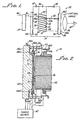
- Night vision device 10 generally comprises a forward objective optical lens assembly 12 (illustrated schematically as a functional block element - which may include one or more lens elements).
- This objective lens 12 focuses incoming light from a distant night-time scene on the front light-receiving end 14a of an I 2 T 14 (as will be seen, this surface is defined by a transparent window portion of the tube - to be further described below).
- the I 2 T provides an image at light output end 14b in phosphorescent yellow-green visible light which replicates the night-time scene.
- This night time scene would generally be not visible (or would be only poorly visible) to a human's diurnal vision.
- This visible image is presented by an eye piece lens illustrated schematically as a single lens 16 producing a virtual image of the rear light-output end of the tube 14 at the user's eye 18.
- I 2 T 14 includes a photocathode 20 which is responsive to photons of infrared light to liberate photoelectrons, a microchannel plate 22 which receives the photoelectrons in a pattern replicating the night-time scene, and which provides an amplified pattern of electrons also replicating this scene, and a display electrode assembly 24.
- the display electrode assembly 24 may be considered as having an aluminized phosphor coating or phosphor screen 26. When this phosphor coating is impacted by the electron shower from microchannel plate 22, it produces a visible image replicating the pattern of the electron shower. Because the electron shower pattern still replicates the scene viewed via lens 12, a user of the device can effectively seen in the dark, by only star light or other low-level illumination.
- a transparent window portion 24a of the assembly 24 conveys the image from screen 26 outwardly of the tube 14 so that it can be presented to the user 18.
- the output electrode assembly may include a charge coupled device (CCD).
- CCD charge coupled device
- the reference numeral 26 would indicate such a CCD, with the output of the image intensifier tube being in the form of an image signal from this CCD.
- the user of such a device would view the image information on a display, such as a liquid crystal display, or cathode ray tube.
- microchannel plate 22 is located just behind photocathode 20, with the microchannel plate 22 having an electron-receiving face 28 and an opposite electron-discharge face 30.
- This microchannel plate 22 further contains a plurality of angulated microchannels 32 which open on the electron-receiving face 28 and on the opposite electron-discharge face 30. Microchannels 32 are separated by passage walls 34.
- Display electrode assembly 24 is typically formed of an aluminized phosphor screen 26 deposited on the vacuum-exposed surface of the optically transparent material of window portion 24a.
- the focusing eye piece lens 16 is located behind the display electrode assembly 24 and allows an observer 18 to view a correctly oriented image corresponding to the initially received low-level image.
- I 2 T 14 the individual components of I 2 T 14 are all mounted and supported in a tube or chamber (to be further explained below) having forward and rear transparent plates cooperating to define a chamber which has been evacuated to a low pressure. This evacuation allows electrons liberated into the free space within the tube to be transferred between the various components by prevailing electrostatic fields without atmospheric interference that could possibly decrease the signal-to-noise ratio.
- photocathode 20 is mounted immediately behind objective lens 12 on the inner vacuum-exposed surface of the window portion of the tube and before microchannel plate 22.
- this photocathode 20 is a circular disk-like structure having a predetermined construction of semiconductor materials, and is mounted on a substrate in a well known manner.
- Suitable photocathode materials are generally semiconductors such as gallium arsenide; or alkali metals, such as compounds of sodium, potassium, cesium, and antimony (commercially available as S-20), carried on a readily available transparent substrate.
- S-20 sulfur-senide
- a variety of glass and fiber optic substrate materials are commercially available.
- photocathode 20 in response to photons 36 entering the forward end of night vision device 10 and passing through objective lens 12, photocathode 20 has an active surface 38 from which are emitted photoelectrons in numbers proportionate to and at locations replicative of the received optical energy of the night-time scene being viewed.
- the image received will be too dim to be viewed with human natural vision, and may be entirely or partially of infrared radiation which is invisible to the human eye.
- the shower of photoelectrons emitted from the photocathode are representative of the image entering the forward end of I 2 T 14.
- the path of a typical photoelectron emitted from the photon input point on the photocathode 20 is represented in Fig. 1 by dashed line 40.
- Photoelectrons 40 emitted from photocathode 20 gain energy through an electric field of predetermined intensity gradient established between photocathode 20 and electron-receiving face 28, which field gradient is provided by power source 42.
- power source 42 will apply an electrostatic field voltage on the order of 200 to 800 volts to create a field of the desired intensity.
- these photoelectrons 40 After accelerating over a distance between the photocathode 20 and the input surface 28 of the microchannel plate 22, these photoelectrons 40 enter microchannels 32 of microchannel plate 22.
- the photoelectrons 40 are amplified by emission of secondary electrons to produce a proportionately larger number of electrons upon passage through microchannel plate 22.
- This amplified shower of secondary-emission electrons 44 also accelerated by a respective electrostatic field generated by power source 46, then exits microchannels 32 of microchannel plate 22 at electron-discharge face 30.
- the amplified shower of photoelectrons and secondary emission electrons is again accelerated in an established electrostatic field provided by power source 48.
- This field is established between the electron-discharge face 30 and display electrode assembly 24.
- the power source 48 produces a field on the order of 3,000 to 7,000 volts, and more preferably on the order of 6,000 volts in order to impart the desired energy to the multiplied electrons 44.
- the shower of photoelectrons and secondary-emission electrons 44 (those ordinarily skilled in the art will know that considered statistically, the shower 44 is almost or entirely devoid of photoelectrons and is made up entirely or almost entirely of secondary emission electrons. Statistically, the probability of a photoelectron avoiding absorption in the microchannels 32 is low). However, the shower 44 is several orders of magnitude more intense than the initial shower of photoelectrons 40, but is still in a pattern replicating the image focused on photocathode 20. This amplified shower of electrons falls on the phosphor screen 26 of display electrode assembly 24 to produce an image in visible light.
- the I 2 T 14 is seen to include a tubular body 50, which is closed at opposite ends by a front light-receiving window 52, and by a rear fiber-optic image output window 54.
- the window 54 defines the light output surface 14b for the tube 14, and carries the coating 26, as will be further described.
- the rear window 54 may be an image-inverting type (i.e., with optical fibers bonded together and rotated 180° between the opposite faces of this window 54 in order to provide an erect image to the user 18.
- the window member 54 is not necessarily of such inverting type. Both of the windows 52 and 54 are sealingly engaged with the body 50, so that an interior chamber 56 of the body 50 can be maintained at a vacuum relative to ambient.
- the tubular body 50 is made up of plural metal rings, each indicated with the general numeral 58 with an alphabetical suffix added thereto (i.e., 58a, 58b, 58c, and 58d) as is necessary to distinguish the individual rings from one another.
- the tubular body sections 58 are spaced apart and are electrically insulated from one another by interposed insulator rings, each of which is indicated with the general numeral 60, again with an alphabetical suffix added thereto (i.e., 60a, 60b, and 60c).
- the sections 58 and insulators 60 are sealingly attached to one another.
- End sections 58a and 58d are likewise sealingly attached to the respective windows 52 and 54.
- a power supply 62 which provides sources 42, 46, and 48, as described above, and which is effective during operation of the I 2 T 14 to maintain an electrostatic field most negative at the section 58a and most positive at the section 58d.
- the front window 52 carries on its rear surface within the chamber 56 the photocathode 20.
- the section 58a is electrically continuous with the photocathode by use of a thin metallization (indicated with reference numeral 58a') extending between the section 58a and the photocathode 20.
- a thin metallization indicated with reference numeral 58a'
- the photocathode by this electrical connection and because of its semi-conductive nature, has an electrostatic charge distributed across the areas of this disk-like photocathode structure.
- a conductive coating or layer is provided at each of the opposite faces 28 and 30 of the microchannel plate 22 (as is indicated by arrowed numerals 28a and 30a).
- Power supply 46 is conductive with these coatings by connection to housing sections 58b and 58c.
- the power supply 48 is conductive with a conductive layer or coating (possibly an aluminum metallization, as mentioned above) at the display electrode assembly 24 by use of a metallization also extending across the vacuum-exposed surfaces of the window member 54, as is indicated by arrowed numeral 54a.
- image intensifier tube is used in a generic sense.
- the tube being powered may be configured as an electron multiplier tube in which the output is an electrical signal rather than a visible image.
- the tube being powered may be of the photodetector, phosphorescence detector, or scintillation detector type, in which the output is also an electrical signal rather than a visible image.
- Such tubes are generally used, for example, to detect a phosphorescent response in a chemical reagent exposed to exciting light of another color or wavelength, or in a detector for high-energy events having as a result of their occurrence the production of a small number of photons (i.e., as few as one photon per event).
- tubes having a photocathode and a dynode may experience some or all of the difficulties in operation which are described above in the context of night vision devices. Accordingly, it will be appreciated that a power supply embodying principles of this invention may be used in such applications.
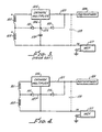
- Figure 3 is a section of a prior art power supply used to deliver high voltage to the photocathode of a prior art night vision device.
- the power supply section includes secondary windings 101 and 103 of a power supply's transformer (the primary winding of which is not shown). Winding 103 is a low voltage winding, while winding 101 is high voltage winding, and these are connected in series as seen in Figure 3.
- the output from the high voltage winding 101 is delivered to a cathode multiplier circuit 105. As is well known in the art, this circuit multiplies and rectifies the series combination voltage received from the windings 101 and 103. The output of the cathode multiplier 105 is delivered through a resistor 107 to the photocathode 109.
- the prior art power supply section shown in Figure 3 also includes a clamping circuit.
- This circuit consists of the low voltage winding 103 being rectified by a diode 111 and filtered by a capacitor 113. The DC voltage developed across the capacitor 113 is then used to clamp the voltage on the photocathode 109 through the use of a clamping diode 115.
- the common connection 106 to the cathode multiplier 105 is also connected to this DC voltage.
- the circuit shown in Figure 3 also shows an MCP 117.
- the intrinsic capacitance between the photocathode 109 and the MCP 117 is shown as a dotted-line capacitor 119.
- the cathode multiplier 105 in Figure 3 operates to multiple and rectify the high voltage coming from the winding 101.
- the output of the cathode multiplier 105 is delivered to the photocathode 109 through the voltage-dropping resistor 107.
- the current through the photocathode 109 also increases.
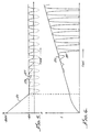
- FIG. 5 This relationship between the current which is traveling through the photocathode 109 and the voltage which is delivered to it during low-to-modest scene intensities is illustrated by line segment 121 in Fig. 5.
- the X axis of Fig. 5 represents time.
- the Y axis of Fig. 5 represents the voltage being delivered to the photocathode.
- the photocathode 109 will effectively stop functioning if the voltage applied to it is less than its charge voltage.
- the clamping diode 105 turns on when the voltage to the photocathode 109 goes below a pre-determined threshold (e.g., 40 volts).
- the pre-determined threshold is designed to be higher than the charge voltage of the photocathode. Once the clamping diode 115 turns on, it effectively clamps the voltage delivered to the photocathode 109 to the clamping voltage developed across the capacitor 113, less the voltage drop of the clamping diode 115.
- Line 125 in Figure 6 illustrates the current which is traveling through the photocathode 109 while the voltage to the photocathode 109 is varying as shown in lines 121 and 123 in Figure 5.
- the current to the photocathode 109 continues to climb after the voltage is clamped.
- the level of the clamping voltage must be set to insure continued operation of all photocathodes to which the circuitry in Figure 3 is connected, and because of substantial variations in the charge voltage of these photocathodes, the clamping level must by necessity be substantially higher than the charge voltages for most of the photocathodes. As shown in Figure 6, this causes the current through the photocathode 109 to increase substantially with increasing scene intensities, even after the clamping level is reached. In turn, this causes undesirable degradation in the resolution and reliability of the photocathode 109.
- FIG 4 is a schematic illustration of a section of a power supply used to deliver high voltage to the photocathode of a night vision device made in accordance with one embodiment of the present invention. As should be apparent, it is the exact same circuit shown in Figure 3, with two modifications.
- the common connection 106 from the cathode multiplier 105 is connected directly to the input to the MCP 117; and the filtering capacitor 113 has been removed.
- a clamping voltage is also developed at point 127 in Figure 4. Unlike the DC clamping voltage which is developed at point 123 in Figure 3, however, it is a time-varying AC voltage at point 127 in Figure 4. The reason for this difference, of course, is the removal of the filtering capacitor 113 from the circuit shown in Figure 3.
- the operation of the circuit in Figure 4 is the same as the operation of the circuit in Figure 3.
- the voltage to the photocathode 109 continues to decrease as a function of the current traveling through the photocathode 109, as shown by the line segment 121 in Figure 5.
- a significant difference materializes.
- a time varying clamping voltage 127 is instead applied, all as shown in Figure 5.
- the magnitude of the variations in the time-varying clamping voltage 127 continue to increase as the intensity of the scene continues to increase until the variations approximate the appearance of a half-wave rectified sine wave, as also shown in Figure 5.
- the falling edges of the time-varying waveform are softened by the residual current contained in the effective capacitance 119 between the photocathode 109 and the MCP 117.
- This time-varying voltage is delivered to the photocathode 109 even during periods when the scene intensity and thus average current through the photocathode 109 is not changing.
Landscapes
- Image-Pickup Tubes, Image-Amplification Tubes, And Storage Tubes (AREA)
Claims (10)
- Combinaison d'un tube amplificateur d'image (14) et d'un circuit d'alimentation en courant (42, 46, 48), le tube amplificateur d'image fournissant une image visible de la scène en cours de visionnage, le tube amplificateur d'image incluant une photocathode (20) recevant des photons de la scène et relâchant des photo-électrons selon un motif reproduisant la scène, une plaque de micro-canal (22) recevant les photo-électrons et fournissant une pluie d'électrons d'émission secondaire selon un motif reproduisant la scène, et un écran (26) recevant la pluie d'électrons d'émission secondaire et produisant une image visible reproduisant la scène; la combinaison du tube incluant une source de courant électrique à un niveau de tension sélectionné, et un circuit d'alimentation en courant recevant ledit courant électrique au dit niveau de tension sélectionné pour fournir en réponse un courant électrique à un niveau de tension plus élevé à ladite photocathode, aux faces opposées de ladite plaque de micro-canal, et au dit écran, caractérisée en ce que ledit circuit d'alimentation en courant inclut également un moyen pour alimenter ladite photocathode audit niveau de tension plus élevé substantiellement redressé en onde sinusoïdale mono alternée.
- Dispositif selon la revendication 1, caractérisé en ce que le circuit d'alimentation en courant inclut un moyen de fournir un niveau de tension d'onde sinusoïdale mono alternée à la photocathode pendant les périodes où l'intensité moyenne de luminosité de la scène est supérieure à un niveau sélectionné et où une réduction du courant de la photocathode est nécessaire pour compenser.
- Circuit d'alimentation en courant selon la revendication 1, caractérisé en ce que le dit circuit d'alimentation en courant inclut un moyen pour alimenter la photocathode en haute tension substantiellement redressée en onde sinusoïdale mono alternée pendant les périodes où la brillance moyenne de la scène est supérieure à un niveau déterminé et où une réduction du courant alimentant la photocathode est nécessaire pour compenser.
- Circuit d'alimentation en courant selon la revendication 2 ou 3, caractérisé en ce que ledit circuit d'alimentation en courant inclut un circuit d'écrêtement ayant une source de courant alternatif.
- Circuit d'alimentation en courant selon la revendication 4, caractérisé en ce que le circuit d'écrêtement inclut une source basse tension (103) et une source haute tension (101), et une diode (111) reliée à un raccordement intermédiaire entre la dite source basse tension et la dite source haute tension et la dite photocathode.
- Circuit d'alimentation en courant selon la revendication 5, caractérisé en ce que le circuit d'écrêtement inclut deux diodes (111, 115) connectées en série à la photocathode et à un raccordement intermédiaire entre la source basse tension et la source haute tension.
- Méthode de réduction du courant alimentant la photocathode d'un tube amplificateur d'image selon la revendication 1, où la dite photocathode reçoit de la lumière de la scène dont l'intensité moyenne est égale ou supérieure à une certaine valeur, la dite méthode incluant l'étape d'application à la dite photocathode d'une tension variable dans le temps ayant tension ondulatoire qui est essentiellement une onde sinusoïdale mono alternée.
- Méthode selon la revendication 7, caractérisée en ce que l'étape d'application à la dite photocathode d'une tension variable dans le temps ayant tension ondulatoire essentiellement sinusoïdale mono alternée est réalisée par l'inclusion dans le circuit d'alimentation en courant d'une paire de sources de tension, où une des sources de tension est une source basse tension et l'autre est une source haute tension.
- Méthode selon la revendication 8, caractérisée en ce que l'étape d'application à la dite photocathode d'une tension variable dans le temps ayant tension ondulatoire essentiellement sinusoïdale mono alternée est réalisée par la connexion en série de l'une des deux sources de tension et de l'autre source de tension, et par la connexion d'une diode entre un raccord intermédiaire entre lesdites deux sources de voltages reliées en série et la dite photocathode.
- Méthode selon la revendication 7, caractérisée en ce que l'étape d'application à la dite photocathode d'une tension variable dans le temps ayant tension ondulatoire essentiellement sinusoïdale mono alternée est réalisée par la limitation de la capacité réelle de filtrage entre ladite photocathode et une plaque de micro-canal du dispositif de vision de nuit essentiellement à la seule capacité inhérente offerte par la juxtaposition de la photocathode et la plaque de micro-canal elles-mêmes, et substantiellement sans aucun ajout d'un condensateur de filtrage distinct.
Applications Claiming Priority (3)
| Application Number | Priority Date | Filing Date | Title |
|---|---|---|---|
| US08/901,424 US5942747A (en) | 1997-07-28 | 1997-07-28 | Night vision device with voltage to photocathode having a rectified half-sine wave component |
| US901424 | 1997-07-28 | ||
| PCT/US1998/015357 WO1999005698A1 (fr) | 1997-07-28 | 1998-07-15 | Appareil de vision nocturne dans lequel une tension variant dans le temps est appliquee a la photocathode |
Publications (3)
| Publication Number | Publication Date |
|---|---|
| EP1000438A1 EP1000438A1 (fr) | 2000-05-17 |
| EP1000438A4 EP1000438A4 (fr) | 2000-08-02 |
| EP1000438B1 true EP1000438B1 (fr) | 2004-07-07 |
Family
ID=25414156
Family Applications (1)
| Application Number | Title | Priority Date | Filing Date |
|---|---|---|---|
| EP98937070A Expired - Lifetime EP1000438B1 (fr) | 1997-07-28 | 1998-07-15 | Combination de renforcateur de l'image et circuit d'alimentation en courant avec une tension variant dans le temps appliquée à la photocathode |
Country Status (4)
| Country | Link |
|---|---|
| US (1) | US5942747A (fr) |
| EP (1) | EP1000438B1 (fr) |
| IL (1) | IL133204A (fr) |
| WO (1) | WO1999005698A1 (fr) |
Families Citing this family (7)
| Publication number | Priority date | Publication date | Assignee | Title |
|---|---|---|---|---|
| US6278104B1 (en) | 1999-09-30 | 2001-08-21 | Litton Systems, Inc. | Power supply for night viewers |
| GB201116778D0 (en) * | 2011-09-29 | 2011-11-09 | Secr Defence | Bright source protection for image intensification devices |
| US9230783B2 (en) * | 2012-06-28 | 2016-01-05 | Exelis, Inc. | Clamped cathode power supply for image intensifier |
| US8872094B2 (en) * | 2012-07-25 | 2014-10-28 | The Boeing Company | Microplasma night vision device |
| EP3171388A1 (fr) * | 2015-11-18 | 2017-05-24 | Université de Strasbourg | Tube intensificateur d'image à sélection temporelle |
| US10734183B2 (en) * | 2018-12-18 | 2020-08-04 | Elbit Systems Of America, Llc | Digital shutter control for bright flash recover in night vision equipment |
| US11101119B2 (en) | 2018-12-20 | 2021-08-24 | Elbit Systems Of America, Llc | Usage and temperature compensation of performance parameters for night vision device |
Citations (2)
| Publication number | Priority date | Publication date | Assignee | Title |
|---|---|---|---|---|
| US2991366A (en) * | 1957-11-29 | 1961-07-04 | Salzberg Bernard | Semiconductor apparatus |
| US4804901A (en) * | 1987-11-13 | 1989-02-14 | Kilo-Watt-Ch-Dog, Inc. | Motor starting circuit |
Family Cites Families (7)
| Publication number | Priority date | Publication date | Assignee | Title |
|---|---|---|---|---|
| US4037132A (en) * | 1976-01-06 | 1977-07-19 | International Telephone And Telegraph Corporation | Image tube power supply |
| US4442349A (en) * | 1980-09-15 | 1984-04-10 | Baird Corporation | Circuitry for the generation and synchronous detection of optical pulsed signals |
| US4882481A (en) * | 1988-10-19 | 1989-11-21 | Sperry Marine Inc. | Automatic brightness control for image intensifiers |
| US4952793A (en) * | 1989-04-14 | 1990-08-28 | Sperry Marine Inc. | Circuit for gating an image intensifier |
| US4935616A (en) * | 1989-08-14 | 1990-06-19 | The United States Of America As Represented By The Department Of Energy | Range imaging laser radar |
| US5146077A (en) * | 1991-03-19 | 1992-09-08 | Itt Corporation | Gated voltage apparatus for high light resolution and bright source protection of image intensifier tube |
| US5336881A (en) * | 1993-03-01 | 1994-08-09 | Itt Corporation | High light resolution control of an image intensifier tube |
-
1997
- 1997-07-28 US US08/901,424 patent/US5942747A/en not_active Expired - Lifetime
-
1998
- 1998-07-15 EP EP98937070A patent/EP1000438B1/fr not_active Expired - Lifetime
- 1998-07-15 WO PCT/US1998/015357 patent/WO1999005698A1/fr active IP Right Grant
- 1998-07-15 IL IL13320498A patent/IL133204A/xx not_active IP Right Cessation
Patent Citations (2)
| Publication number | Priority date | Publication date | Assignee | Title |
|---|---|---|---|---|
| US2991366A (en) * | 1957-11-29 | 1961-07-04 | Salzberg Bernard | Semiconductor apparatus |
| US4804901A (en) * | 1987-11-13 | 1989-02-14 | Kilo-Watt-Ch-Dog, Inc. | Motor starting circuit |
Also Published As
| Publication number | Publication date |
|---|---|
| US5942747A (en) | 1999-08-24 |
| EP1000438A1 (fr) | 2000-05-17 |
| EP1000438A4 (fr) | 2000-08-02 |
| IL133204A (en) | 2005-12-18 |
| IL133204A0 (en) | 2001-03-19 |
| WO1999005698A1 (fr) | 1999-02-04 |
Similar Documents
| Publication | Publication Date | Title |
|---|---|---|
| US5146077A (en) | Gated voltage apparatus for high light resolution and bright source protection of image intensifier tube | |
| CA2458532C (fr) | Detecteur a semiconducteur hybride intensifie | |
| US6278104B1 (en) | Power supply for night viewers | |
| US5949063A (en) | Night vision device having improved automatic brightness control and bright-source protection, improved power supply for such a night vision device, and method of its operation | |
| US5510673A (en) | Shock resistant cascaded microchannel plate assemblies and methods of use | |
| US4603250A (en) | Image intensifier with time programmed variable gain | |
| US5883381A (en) | Night vision device having series regulator in power supply for MCP voltage control | |
| EP1000438B1 (fr) | Combination de renforcateur de l'image et circuit d'alimentation en courant avec une tension variant dans le temps appliquée à la photocathode | |
| US4924080A (en) | Electromagnetic interference protection for image intensifier tube | |
| US6624414B1 (en) | Image intensifier tube with IR up-conversion phosphor on the input side | |
| JP2003520389A (ja) | ナイト・ビジョン・デバイス及び方法 | |
| US6040000A (en) | Method and apparatus for a microchannel plate having a fissured coating | |
| EP1057208B1 (fr) | Appareil de vision nocturne a tube intensificateur d'image | |
| US6320180B1 (en) | Method and system for enhanced vision employing an improved image intensifier and gated power supply | |
| US6049168A (en) | Method and system for manufacturing microchannel plates | |
| US7462090B1 (en) | Method and system for detecting radiation incorporating a hardened photocathode | |
| US3665247A (en) | Power regulating means for light amplifier tubes | |
| EP0619596B1 (fr) | Intensificateur d'images | |
| US6297494B1 (en) | Method and system for enhanced vision employing an improved image intensifier with a gated power supply and reduced halo | |
| Verona | Image intensifiers: Past and present | |
| Stoudenheimer | Image intensifier developments in the RCA electron tube division | |
| US2203225A (en) | Electron discharge device utilizing electron multiplication | |
| US2774901A (en) | Tube for electro-magnetic images | |
| Karim et al. | Intensifier and Cathode-Ray Tube Technologies | |
| RU2187169C2 (ru) | Электронно-оптический преобразователь |
Legal Events
| Date | Code | Title | Description |
|---|---|---|---|
| PUAI | Public reference made under article 153(3) epc to a published international application that has entered the european phase |
Free format text: ORIGINAL CODE: 0009012 |
|
| 17P | Request for examination filed |
Effective date: 20000225 |
|
| AK | Designated contracting states |
Kind code of ref document: A1 Designated state(s): NL |
|
| A4 | Supplementary search report drawn up and despatched |
Effective date: 20000616 |
|
| AK | Designated contracting states |
Kind code of ref document: A4 Designated state(s): NL |
|
| RIC1 | Information provided on ipc code assigned before grant |
Free format text: 7H 01J 40/14 A, 7H 01J 29/98 B, 7H 01J 31/50 B |
|
| 17Q | First examination report despatched |
Effective date: 20030211 |
|
| RTI1 | Title (correction) |
Free format text: IMAGE INTENSIFIER TUBE AND POWER SUPPLY CIRCUIT COMBINATION WITH TIME-VARYING VOLTAGE TO THE PHOTOCATHODE |
|
| GRAP | Despatch of communication of intention to grant a patent |
Free format text: ORIGINAL CODE: EPIDOSNIGR1 |
|
| GRAS | Grant fee paid |
Free format text: ORIGINAL CODE: EPIDOSNIGR3 |
|
| GRAA | (expected) grant |
Free format text: ORIGINAL CODE: 0009210 |
|
| AK | Designated contracting states |
Kind code of ref document: B1 Designated state(s): NL |
|
| PLBE | No opposition filed within time limit |
Free format text: ORIGINAL CODE: 0009261 |
|
| STAA | Information on the status of an ep patent application or granted ep patent |
Free format text: STATUS: NO OPPOSITION FILED WITHIN TIME LIMIT |
|
| 26N | No opposition filed |
Effective date: 20050408 |
|
| REG | Reference to a national code |
Ref country code: NL Ref legal event code: TD Effective date: 20100705 |
|
| PGFP | Annual fee paid to national office [announced via postgrant information from national office to epo] |
Ref country code: NL Payment date: 20170719 Year of fee payment: 20 |
|
| REG | Reference to a national code |
Ref country code: NL Ref legal event code: MK Effective date: 20180714 |