EP0993159A2 - Schätzung von Trägerfrequenzverschiebung - Google Patents
Schätzung von Trägerfrequenzverschiebung Download PDFInfo
- Publication number
- EP0993159A2 EP0993159A2 EP99119399A EP99119399A EP0993159A2 EP 0993159 A2 EP0993159 A2 EP 0993159A2 EP 99119399 A EP99119399 A EP 99119399A EP 99119399 A EP99119399 A EP 99119399A EP 0993159 A2 EP0993159 A2 EP 0993159A2
- Authority
- EP
- European Patent Office
- Prior art keywords
- symbol
- subsection
- denoted
- frequency offset
- analog
- Prior art date
- Legal status (The legal status is an assumption and is not a legal conclusion. Google has not performed a legal analysis and makes no representation as to the accuracy of the status listed.)
- Granted
Links
Images


Classifications
-
- H—ELECTRICITY
- H04—ELECTRIC COMMUNICATION TECHNIQUE
- H04L—TRANSMISSION OF DIGITAL INFORMATION, e.g. TELEGRAPHIC COMMUNICATION
- H04L27/00—Modulated-carrier systems
- H04L27/18—Phase-modulated carrier systems, i.e. using phase-shift keying
- H04L27/22—Demodulator circuits; Receiver circuits
Definitions
- the present invention relates to a method for rapid carrier frequency estimation in a communication system.
- Communication systems feature a transmitter and a receiver. In order for communication to occur, a transmitted signal must be accurately processed by the receiver for accurate recovery of the information contained within the signal.
- radio frequency signals are subject to distortion such as amplitude and phase distortion and carrier frequency offset.
- Amplitude and phase distortion which cause time dispersion, are known as channel response.
- the transmission frame may include synchronization fields, which are required for correct processing of the frame to overcome the above-mentioned distortions, yet which must be minimized in order to maximize the available bandwidth.
- each burst may include synchronization fields. For example, these fields may appear at the beginning of the burst, and then they form the header.
- the synchronization overhead must be decreased as much as possible, such that the synchronization field must be as short as is practical.
- Part of the processing of the synchronization field involves the estimation of the carrier frequency offset.
- the frequencies by which the signal are modulated, upconverted, downconverted and demodulated have some deviation from their ideal values. The sum of all these deviations is the carrier frequency offset
- the estimation of the carrier frequency offset is necessary for processing the received signal. Methods for rapidly estimating the carrier frequency offset in the presence of channel distortion such as ISI (intersymbol interference) would therefore be very useful.
- the analog-to-digital processing unit features an analog-to-digital converter and Y i is an output of the analog-to-digital converter.
- the analog-to-digital processing unit features a receive filter and Y i is an output of the receive filter.
- the steps of the method are repeated for a plurality of frames n , such that a plurality of n frequency offsets is calculated, the method further comprising the step of: (g) averaging the plurality of n frequency offsets to obtain the frequency offset
- a method for estimating a frequency offset of at least one frame containing at least one synchronization field being divided into at least a first subsection and a second subsection separated by a spacer portion, the at least two subsections being composed of substantially equivalent pseudorandom symbols, the first subsection featuring at least three portions, a first portion having a first symbol denoted symbol i 1 , a second portion having a first symbol denoted symbol i 2 and a last symbol denoted symbol i 3 , and a third portion having a last symbol denoted symbol i 4 , the second subsection also featuring at least three portions, a first portion having a first symbol denoted symbol i 5 , a second portion having a first symbol denoted symbol i 6 and a last symbol denoted symbol i 7 , and a third portion having a last symbol denoted symbol i 8 , the frame being received by a receiver from a transmitter, the receiver including at least an analog-to-digital processing unit
- a signal which corresponds to a particular burst S i ( i being an integer) is defined as having been produced by processing at least a portion of burst S i , for example by sampling an analog signal obtained from the received burst S i to produce a "corresponding" digital sampled signal.
- the present invention is of a method for precise and rapid estimation of the carrier frequency offset for a communication system which includes a transmitter and a receiver.
- the method of the present invention estimates the carrier frequency offset from the synchronization field, which preferably features a sequence of pseudorandom symbols which appears at least twice within the synchronization field.
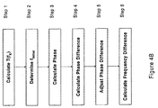
- the phase angle for each of these repeated sequences is then used to determine the phase difference, from which the frequency offset is calculated.
- the method also includes a coarse frequency estimate which is performed first, for example if the frequency offset is particularly large.
- FIG. 1 shows an exemplary system for communication according to the background art.
- a system 10 features a transmitter 12 and a receiver 14 .
- Radio-frequency signals are transmitted from transmitter 12 and are received by receiver 14 , although of course other types of signals could be substituted.
- the method of the present invention would also be suitable for voice-band modems.
- the following discussion centers upon radio-frequency signals without intending to be limiting in any way.
- the signal originates as a digital signal which is processed by transmitter 12 to yield an analog radio-frequency signal before transmission. As described in greater detail below, this processing includes encoding, digital to analog conversion, modulation and then upconversion to the frequency of the transmitted signal.
- Receiver 14 receives this analog signal, and then downconverts and demodulates the signal. This demodulated signal is then processed to obtain a digital signal output. The steps of processing the demodulated signal attempt to obtain a digital signal output which is as similar as possible to the original digital signal input at transmitter 12 . Again, as described in greater detail below, this processing includes downconversion, demodulation, analog to digital conversion, further processing and then decoding. The further processing is necessary because the analog signal which is received by receiver 14 is not identical to the analog signal which was transmitted by transmitter 12 . Alterations occur to the analog signal as a result of interference, radio-frequency carrier offsets and channel response.
- transmitter 12 receives a digital input which is received by an encoder 30 .
- Encoder 30 maps the digital bitstream input into symbols.
- a "symbol” is a k -bit sized chunk into which the transmission signal is divided.
- the digital signal is then split into two signal components designated as "I” (in phase) and "Q" (quadrature). Each digital signal component is preferably filtered by one of two digital transmit filters 32 .
- the digital signal is converted to an analog signal by one of two digital-to-analog converters 34 .
- the analog signal is then filtered by one of two analog low pass filters 36 , designated as "LPF".
- Radio-frequency transmitter unit 38 preferably includes a modulator 40 and a radio-frequency upconverter 42 .
- Modulator 40 combines the "I” and “Q” components together and modulates these components on a chosen carrier, such that the signal is now an intermediate frequency signal.
- Radio-frequency upconverter 42 is required to convert the intermediate frequency signal to the frequency of the transmitted radio-frequency signal, which is typically a higher value than the frequency of the intermediate frequency signal.
- Radio-frequency receiver unit 24 preferably includes a radio-frequency downconverter 44 and a demodulator 46 .
- Radio-frequency downconverter 44 is required to convert the frequency of the transmitted radio-frequency signal to an intermediate frequency signal.
- the intermediate frequency signal passes to demodulator 46 , which splits the signal into the two components of "I" and "Q".
- the digital signals then are further processed by one of two digital receive filters 52 .
- digital receive filters 52 filter noise to improve the signal to noise ratio.
- analog-to-digital converters 50 and digital receive filters 52 are also collectively designated an “analog-to-digital processing unit 53 ".
- the filtered signal is passed to a receiver back-end 54 to produce a digital output during steady state processing of the signal.
- the method of the present invention is preferably operative during the processing of the synchronization field itself, more preferably before an equalizer has been trained, if such an equalizer is present, and hence more preferably before the signal is equalized.
- the digital processing within receiver back-end 54 includes compensation for both carrier frequency offset and phase offset, and for ISI (intersymbol interference).
- the method of the present invention enables the carrier frequency offset to be estimated much more rapidly and with shorter synchronization fields (described with regard to Figure 3), as described in greater detail below with regard to Figures 4A and 4B.
- every frame 70 includes a synchronization field 72 and a traffic portion 74 (as illustrated, relative proportions are not shown).
- Synchronization field 72 is present for rapid and efficient synchronization.
- Synchronization field 72 preferably appears at the beginning of frame 70 , in which case synchronization field 72 is the "header" of frame 70 .
- Synchronization field 72 is optionally divided into at least two subsections 76 and 77 , each of which contains a predefined sequence of pseudorandom symbols, and which are preferably substantially equivalent, such that the processing of both subsections 76 and 77 would preferably yield the same or substantially similar ISI .
- Each subsection 76 and 77 is preferably separated by a spacer portion 78 which is at least of a predefined length. More preferably, the length of spacer portion 78 is preferably similar to that of one subsection 76 or 77 .
- each subsection 76 or 77 is further divided into at least three sequences of pseudorandom symbols 80 (hereinafter collectively referred as "sequences 80 "), each of which can also be described as a portion of each subsection 76 or 77 .
- sequences 80 are composed of a plurality of symbols.
- each of the three sequences 80 is a different sequence of pseudorandom symbols.
- a first sequence 82 of the three sequences 80 is substantially equivalent for both first subsection 76 (designated as "subsection 1") and for second subsection 77 (designated as "subsection 2").
- a second sequence 84 is substantially equivalent for both first subsection 76 and for second subsection 77
- a third sequence 86 is also substantially equivalent for both first subsection 76 and for second subsection 77 .
- the first symbol for first sequence 82 is symbol i 1 ; the first symbol for second sequence 84 is symbol i 2 ; the last symbol for second sequence 84 is symbol i 3 ; and the last symbol for third sequence 86 is symbol i 4 .
- the first symbol for first sequence 82 is symbol i 5 ; the first symbol for second sequence 84 is symbol i 6 ; the last symbol for second sequence 84 is symbol i 7 ; and the last symbol for third sequence 86 is symbol i 8 .
- first sequence 82 and third sequence 86 are both preferably included to minimize distortions of the symbols of second sequence 84 from previous and following symbols, such that symbols i 2 through i 3 and symbols i 6 through i 7 are both distorted by ISI to the same, or to a substantially similar, degree.
- the presence of first sequence 82 of a sufficient length enables the ISI caused by symbols prior to symbol i 1 to have substantially decayed by the time symbol i 2 is received.
- third sequence 86 has a sufficient length, then ISI caused by symbols after symbol i 4 does not substantially affect symbol i 3 .
- first sequence 82 and third sequence 86 act as ISI buffers for second sequence 84 .
- the signal processing is at the stage when synchronization field 72 only is being processed by the receiver of a receiver-transmitter pair, and the equalizer is not yet operative, if such an equalizer is present. Therefore, the signal being processed still has ISI (intersymbol interference), and inaccuracies of channel response. More preferably, the signal has already been processed by the receive filters of Figure 2B, although alternatively the signal could be received directly from the analog-to-digital converters for processing according to the method of the present invention. Furthermore, more preferably synchronization field 72 is the header of frame 70 . The type of transmission is optionally bursty, such that frame 70 is a burst, or alternatively the transmissions could be continuous.
- the timing of the reception of synchronization field 72 by the receiver of the receiver-transmitter pair must be predetermined, such that a particular transmission structure is predetermined and is known in advance by the receiver.
- the receiver itself could control or determine the transmission structure.
- timing of the sampling of the analog-to-digital converter is not necessarily optimal, the timing must at least be consistent from subsection 1 to subsection 2. Optimal timing is preferred because the method of the present invention gives better performance with such optimal timing. If the timing is not optimal but is consistent, then preferably the sampling rate is greater than one sample per symbol, in order to overcome any deficiencies of the sampling timing.
- One example of a system in which timing is consistent but not optimal is given in the U.S. Patent Application filed on the same day as this Application, entitled “Method For Rapid Synchronization Of A Point to Multipoint Communication System" and incorporated by reference as if fully set forth herein.
- the sampling timing is set by the base station transmit clock, such that the sampling timing of the terminal station and base station receive clocks is set according to the base station transmit clock, and such that the terminal station transmit clock is also determined according to the base station transmit clock.
- the base station timing is known and is consistent, but is not necessarily optimal.
- the steps of the method of the present invention are performed as follows, preferably by a data processor in receiver back-end 54 , for example as software being stored on a non-volatile memory in receiver back-end 54 .
- the steps of the method of the present invention could be performed by dedicated hardware, or by a combination of hardware and software, also known as "firmware".
- firmware One of ordinary skill in the art could easily implement the method of the present invention for functioning as software, hardware, or firmware.
- the steps of the method are performed by a receiver which receives at least one frame, containing at least one synchronization field, from a transmitter.
- Bold font indicates column vectors, while elements of a vector are in regular font with a subscript.
- Y is designated as either the output of the receive filter or alternatively of the analog-to-digital converter from processing the header, since the values of Y are optionally and preferably received from the receive filter, or alternatively are directly received from the analog-to-digital converter.
- This calculated frequency difference is the carrier frequency offset, which could be used for the remaining processing of the signal as shown in Figure 2B
- these calculations are repeated each time a synchronization field is sent. More preferably, the synchronization field is repeatably transmitted n times, such that n estimates of the carrier frequency offset are calculated and are then averaged to obtain a weighted carrier frequency offset estimate.
- more weight could optionally be given to more recently calculated estimates of the frequency offset, since the frequency varies over time and the more recently calculated estimates of the frequency offset would therefore be based upon more recently received synchronization fields.
- each symbol is sampled once. For example, if the symbol timing recovery is known to be optimal, then this assumption is correct. However, if the symbol timing recovery is known to be consistent but not optimal, then each symbol may be sampled more than once or "oversampled". In this situation, a certain number of samples must be discarded or "downsampled", such that there is only one sample processed per symbol. For example, if each symbol is sampled twice, then one sample must be kept and one sample must be discarded according to a consistent scheme, such that all even samples or all odd samples are discarded for example. Preferably, this consistent scheme is such that the samples are kept at the most optimum phase.
- the advantages of the method of the present invention are as follows. First, the estimate of the phase is degraded both by additive noise and by ISI (intersymbol interference). Since subsections 1 and 2 are identical, both suffer from the same ISI and hence both have the same bias due to ISI. However, since the phase difference is calculated, the bias due to ISI is canceled out of the calculations. Therefore, the method of the present invention remains operative even under conditions of severe ISI and does not require the signal to be equalized.
- ISI symbol interference
- subsections 1 and 2 include one or more sequences of pseudorandom symbols of more than one frequency, to prevent strong attenuation of the received signals if a deep notch exists at a particular frequency.
- sequences of pseudorandom symbols of a plurality of frequencies are suitable for the adaptation of equalizers, thus permitting one synchronization field to be used for both equalizer adaptation and for the estimate of the carrier frequency offset according to the present invention.
- f initial there is an initial frequency offset, f initial , which is used to calculate the estimated frequency offset, which could be obtained from a coarse frequency estimate as described in further detail below.
- f initial an initial frequency offset
- stage 2 the frequency offset estimate itself, or "fine frequency offset estimate" is calculated.
- the frequency offset is greater than 1/(2 ⁇ t)
- the two stage method is strongly preferred.
- the two stage method of the present invention includes the calculation of a coarse frequency offset as f initial prior to the performance of the above steps of the one stage method of the present invention.
- the assumptions are similar to those described above with regard to the method of Figure 4A.
- one example of a two stage method according to the present invention is performed as follows.
- the DFT discrete Fourier transform
- the maximum absolute value in the frequency domain is determined, and the corresponding frequency is then selected as the coarse estimate.
- the set of frequencies ⁇ f k ⁇ between f min and f max is chosen such that the error of the come estimate is no greater than f tol .
- f initial is determined as the value of the frequency f k for which the set of values T( f k ) is maximized.
- This calculated frequency difference is the carrier frequency offset, which could be used for the remaining processing shown in Figure 2.
Landscapes
- Engineering & Computer Science (AREA)
- Computer Networks & Wireless Communication (AREA)
- Signal Processing (AREA)
- Synchronisation In Digital Transmission Systems (AREA)
- Digital Transmission Methods That Use Modulated Carrier Waves (AREA)
- Transmitters (AREA)
- Channel Selection Circuits, Automatic Tuning Circuits (AREA)
- Stabilization Of Oscillater, Synchronisation, Frequency Synthesizers (AREA)
- Monitoring And Testing Of Transmission In General (AREA)
- Radio Relay Systems (AREA)
Applications Claiming Priority (2)
| Application Number | Priority Date | Filing Date | Title |
|---|---|---|---|
| US162996 | 1998-09-30 | ||
| US09/162,996 US6731710B1 (en) | 1998-09-30 | 1998-09-30 | Method for rapid carrier frequency estimation in a communication system |
Publications (3)
| Publication Number | Publication Date |
|---|---|
| EP0993159A2 true EP0993159A2 (de) | 2000-04-12 |
| EP0993159A3 EP0993159A3 (de) | 2002-03-06 |
| EP0993159B1 EP0993159B1 (de) | 2004-07-07 |
Family
ID=22588007
Family Applications (1)
| Application Number | Title | Priority Date | Filing Date |
|---|---|---|---|
| EP99119399A Expired - Lifetime EP0993159B1 (de) | 1998-09-30 | 1999-09-30 | Schätzung von Trägerfrequenzverschiebung |
Country Status (6)
| Country | Link |
|---|---|
| US (1) | US6731710B1 (de) |
| EP (1) | EP0993159B1 (de) |
| AT (1) | ATE270803T1 (de) |
| DE (1) | DE69918508T2 (de) |
| ES (1) | ES2224518T3 (de) |
| IL (1) | IL131951A (de) |
Cited By (3)
| Publication number | Priority date | Publication date | Assignee | Title |
|---|---|---|---|---|
| SG109499A1 (en) * | 2002-06-17 | 2005-03-30 | Oki Techno Ct Singapore Pte | Frequency estimation in a burst radio receiver |
| WO2009152395A3 (en) * | 2008-06-12 | 2010-02-04 | Qualcomm Incorporated | Method and system for carrier frequency offset estimation and correction in ofdm/ofdma systems |
| CN110311874A (zh) * | 2019-07-18 | 2019-10-08 | 锐迪科微电子(上海)有限公司 | 载波频偏确定方法及装置 |
Families Citing this family (8)
| Publication number | Priority date | Publication date | Assignee | Title |
|---|---|---|---|---|
| WO2001081948A2 (en) * | 2000-04-25 | 2001-11-01 | Eskom | Low noise to signal evaluation |
| US7239431B2 (en) * | 2001-04-04 | 2007-07-03 | Agere Systems Inc. | System and method for recovering primary channel operation in a facsimile receiver and facsimile machine incorporating the same |
| DE50105257D1 (de) * | 2001-11-16 | 2005-03-10 | Com Res Gmbh Solutions For Com | Verfahren und System zur Frequenzoffsetschätzung für Trägermodulierte digitale Kommunikationssysteme |
| US7460839B2 (en) | 2004-07-19 | 2008-12-02 | Purewave Networks, Inc. | Non-simultaneous frequency diversity in radio communication systems |
| US7263335B2 (en) | 2004-07-19 | 2007-08-28 | Purewave Networks, Inc. | Multi-connection, non-simultaneous frequency diversity in radio communication systems |
| US8031747B2 (en) | 2009-04-29 | 2011-10-04 | Juniper Networks, Inc. | Apparatus and method of compensating for clock frequency and phase variations by processing packet delay values |
| KR101298591B1 (ko) * | 2009-12-17 | 2013-08-26 | 한국전자통신연구원 | 무선 통신 시스템에서 데이터 송수신 장치 및 방법 |
| KR102025324B1 (ko) * | 2017-09-27 | 2019-09-25 | (주)에프씨아이 | 주파수 오프셋 추정 방법 |
Family Cites Families (3)
| Publication number | Priority date | Publication date | Assignee | Title |
|---|---|---|---|---|
| US6334219B1 (en) * | 1994-09-26 | 2001-12-25 | Adc Telecommunications Inc. | Channel selection for a hybrid fiber coax network |
| SE514986C2 (sv) * | 1995-03-01 | 2001-05-28 | Telia Ab | Metod och anordning för synkronisering vid OFDM-system |
| US6097770A (en) * | 1996-10-31 | 2000-08-01 | Lucent Technologies Inc. | Frequency offset estimation for wireless systems based on channel impulse response |
-
1998
- 1998-09-30 US US09/162,996 patent/US6731710B1/en not_active Expired - Fee Related
-
1999
- 1999-09-16 IL IL13195199A patent/IL131951A/en not_active IP Right Cessation
- 1999-09-30 EP EP99119399A patent/EP0993159B1/de not_active Expired - Lifetime
- 1999-09-30 DE DE69918508T patent/DE69918508T2/de not_active Expired - Lifetime
- 1999-09-30 AT AT99119399T patent/ATE270803T1/de not_active IP Right Cessation
- 1999-09-30 ES ES99119399T patent/ES2224518T3/es not_active Expired - Lifetime
Cited By (3)
| Publication number | Priority date | Publication date | Assignee | Title |
|---|---|---|---|---|
| SG109499A1 (en) * | 2002-06-17 | 2005-03-30 | Oki Techno Ct Singapore Pte | Frequency estimation in a burst radio receiver |
| WO2009152395A3 (en) * | 2008-06-12 | 2010-02-04 | Qualcomm Incorporated | Method and system for carrier frequency offset estimation and correction in ofdm/ofdma systems |
| CN110311874A (zh) * | 2019-07-18 | 2019-10-08 | 锐迪科微电子(上海)有限公司 | 载波频偏确定方法及装置 |
Also Published As
| Publication number | Publication date |
|---|---|
| ES2224518T3 (es) | 2005-03-01 |
| DE69918508D1 (de) | 2004-08-12 |
| EP0993159A3 (de) | 2002-03-06 |
| IL131951A0 (en) | 2001-03-19 |
| EP0993159B1 (de) | 2004-07-07 |
| US6731710B1 (en) | 2004-05-04 |
| DE69918508T2 (de) | 2005-07-28 |
| ATE270803T1 (de) | 2004-07-15 |
| IL131951A (en) | 2004-01-04 |
Similar Documents
| Publication | Publication Date | Title |
|---|---|---|
| EP0683576B1 (de) | Digitales OFDM-Rundfunksystem, sowie Übertragungs- und Empfangsvorrichtung für Digitalrundfunk | |
| US5870438A (en) | Fast resynchronization system for high-speed data transmission | |
| US6584164B1 (en) | Method for forming a training sequence | |
| US6363131B1 (en) | Method and apparatus for joint timing synchronization and frequency offset estimation | |
| EP1313283B1 (de) | Taktsynchronisierung für auf OFDM basierte drahtlose Netzwerke | |
| EP0955754B1 (de) | Verfahren un Anordnung zum Erreichen und Aufrechterhalten der Symbolsynchronisierung in einem OFDM-Übertragungssystem | |
| EP1608122B1 (de) | Verfahren und System zur Kommunikation unter Benutzung übertragener Symbole die mit verschiedenen Zeitdauern assoziiert sind | |
| JP2001268041A (ja) | 直交周波数分割多重システムにおけるサンプリングオフセット補正 | |
| JP2010521939A (ja) | 複数のフィルタバンクを用いる多重搬送波受信機のロバストな同期方法及びそれに対応する受信機とトランシーバ | |
| WO2001020863A9 (en) | Method and apparatus for carrier phase tracking | |
| JPH08237218A (ja) | 周波数同調回路からなる直交周波数分割多重信号用の送信機及び受信機 | |
| EP0851642A2 (de) | Mehrträgerempfänger mit Ausgleich von Frequenzverschiebungen und von frequenzabhängigen Verzerrungen | |
| EP0993159B1 (de) | Schätzung von Trägerfrequenzverschiebung | |
| EP0573696B1 (de) | Taktwiedergewinnungsverfahren und -system | |
| CN112583571B (zh) | 一种信号的采样方法及装置 | |
| WO2007006202A1 (fr) | Système et procédé de transmission qotdma | |
| EP0700189B1 (de) | Verfahren und Vorrichtung für die Entzerrung von digitalen Signalen im Frequenzbereich | |
| EP1780970B1 (de) | Frequenzkorrektur für ein Mehrträgersystem | |
| US7130360B2 (en) | Apparatus and method for receiving digital signal | |
| EP1018253B1 (de) | Abtastfrequenzeinstellung in einem mehrträger-empfänger | |
| US6845133B2 (en) | Method and device for processing signals of a digital transmission system | |
| US8223865B2 (en) | Method for the blind estimation of OFDM signal parameters by adapted filtering | |
| JP2002232389A (ja) | Ofdm受信装置 | |
| JP2001044963A (ja) | 受信装置 | |
| JP2000022660A (ja) | ディジタル通信装置 |
Legal Events
| Date | Code | Title | Description |
|---|---|---|---|
| PUAI | Public reference made under article 153(3) epc to a published international application that has entered the european phase |
Free format text: ORIGINAL CODE: 0009012 |
|
| AK | Designated contracting states |
Kind code of ref document: A2 Designated state(s): AT BE CH CY DE DK ES FI FR GB GR IE IT LI LU MC NL PT SE |
|
| AX | Request for extension of the european patent |
Free format text: AL;LT;LV;MK;RO;SI |
|
| PUAL | Search report despatched |
Free format text: ORIGINAL CODE: 0009013 |
|
| RIC1 | Information provided on ipc code assigned before grant |
Free format text: 7H 04L 27/22 A, 7H 04L 27/227 B, 7H 04L 27/38 B, 7H 04J 3/06 B, 7H 04L 7/04 B |
|
| AK | Designated contracting states |
Kind code of ref document: A3 Designated state(s): AT BE CH CY DE DK ES FI FR GB GR IE IT LI LU MC NL PT SE |
|
| AX | Request for extension of the european patent |
Free format text: AL;LT;LV;MK;RO;SI |
|
| 17P | Request for examination filed |
Effective date: 20020904 |
|
| AKX | Designation fees paid |
Free format text: AT BE CH CY DE DK ES FI FR GB GR IE IT LI LU MC NL PT SE |
|
| GRAP | Despatch of communication of intention to grant a patent |
Free format text: ORIGINAL CODE: EPIDOSNIGR1 |
|
| GRAS | Grant fee paid |
Free format text: ORIGINAL CODE: EPIDOSNIGR3 |
|
| GRAA | (expected) grant |
Free format text: ORIGINAL CODE: 0009210 |
|
| AK | Designated contracting states |
Kind code of ref document: B1 Designated state(s): AT BE CH CY DE DK ES FI FR GB GR IE IT LI LU MC NL PT SE |
|
| PG25 | Lapsed in a contracting state [announced via postgrant information from national office to epo] |
Ref country code: NL Free format text: LAPSE BECAUSE OF FAILURE TO SUBMIT A TRANSLATION OF THE DESCRIPTION OR TO PAY THE FEE WITHIN THE PRESCRIBED TIME-LIMIT Effective date: 20040707 Ref country code: LI Free format text: LAPSE BECAUSE OF FAILURE TO SUBMIT A TRANSLATION OF THE DESCRIPTION OR TO PAY THE FEE WITHIN THE PRESCRIBED TIME-LIMIT Effective date: 20040707 Ref country code: IT Free format text: LAPSE BECAUSE OF FAILURE TO SUBMIT A TRANSLATION OF THE DESCRIPTION OR TO PAY THE FEE WITHIN THE PRESCRIBED TIME-LIMIT;WARNING: LAPSES OF ITALIAN PATENTS WITH EFFECTIVE DATE BEFORE 2007 MAY HAVE OCCURRED AT ANY TIME BEFORE 2007. THE CORRECT EFFECTIVE DATE MAY BE DIFFERENT FROM THE ONE RECORDED. Effective date: 20040707 Ref country code: FI Free format text: LAPSE BECAUSE OF FAILURE TO SUBMIT A TRANSLATION OF THE DESCRIPTION OR TO PAY THE FEE WITHIN THE PRESCRIBED TIME-LIMIT Effective date: 20040707 Ref country code: CY Free format text: LAPSE BECAUSE OF FAILURE TO SUBMIT A TRANSLATION OF THE DESCRIPTION OR TO PAY THE FEE WITHIN THE PRESCRIBED TIME-LIMIT Effective date: 20040707 Ref country code: CH Free format text: LAPSE BECAUSE OF FAILURE TO SUBMIT A TRANSLATION OF THE DESCRIPTION OR TO PAY THE FEE WITHIN THE PRESCRIBED TIME-LIMIT Effective date: 20040707 Ref country code: BE Free format text: LAPSE BECAUSE OF FAILURE TO SUBMIT A TRANSLATION OF THE DESCRIPTION OR TO PAY THE FEE WITHIN THE PRESCRIBED TIME-LIMIT Effective date: 20040707 Ref country code: AT Free format text: LAPSE BECAUSE OF FAILURE TO SUBMIT A TRANSLATION OF THE DESCRIPTION OR TO PAY THE FEE WITHIN THE PRESCRIBED TIME-LIMIT Effective date: 20040707 |
|
| REG | Reference to a national code |
Ref country code: GB Ref legal event code: FG4D |
|
| REG | Reference to a national code |
Ref country code: CH Ref legal event code: EP |
|
| REG | Reference to a national code |
Ref country code: IE Ref legal event code: FG4D |
|
| REF | Corresponds to: |
Ref document number: 69918508 Country of ref document: DE Date of ref document: 20040812 Kind code of ref document: P |
|
| PG25 | Lapsed in a contracting state [announced via postgrant information from national office to epo] |
Ref country code: MC Free format text: LAPSE BECAUSE OF NON-PAYMENT OF DUE FEES Effective date: 20040930 Ref country code: LU Free format text: LAPSE BECAUSE OF NON-PAYMENT OF DUE FEES Effective date: 20040930 Ref country code: IE Free format text: LAPSE BECAUSE OF NON-PAYMENT OF DUE FEES Effective date: 20040930 |
|
| PG25 | Lapsed in a contracting state [announced via postgrant information from national office to epo] |
Ref country code: SE Free format text: LAPSE BECAUSE OF FAILURE TO SUBMIT A TRANSLATION OF THE DESCRIPTION OR TO PAY THE FEE WITHIN THE PRESCRIBED TIME-LIMIT Effective date: 20041007 Ref country code: GR Free format text: LAPSE BECAUSE OF FAILURE TO SUBMIT A TRANSLATION OF THE DESCRIPTION OR TO PAY THE FEE WITHIN THE PRESCRIBED TIME-LIMIT Effective date: 20041007 Ref country code: DK Free format text: LAPSE BECAUSE OF FAILURE TO SUBMIT A TRANSLATION OF THE DESCRIPTION OR TO PAY THE FEE WITHIN THE PRESCRIBED TIME-LIMIT Effective date: 20041007 |
|
| NLV1 | Nl: lapsed or annulled due to failure to fulfill the requirements of art. 29p and 29m of the patents act | ||
| REG | Reference to a national code |
Ref country code: CH Ref legal event code: PL |
|
| REG | Reference to a national code |
Ref country code: ES Ref legal event code: FG2A Ref document number: 2224518 Country of ref document: ES Kind code of ref document: T3 |
|
| PLBE | No opposition filed within time limit |
Free format text: ORIGINAL CODE: 0009261 |
|
| STAA | Information on the status of an ep patent application or granted ep patent |
Free format text: STATUS: NO OPPOSITION FILED WITHIN TIME LIMIT |
|
| ET | Fr: translation filed | ||
| 26N | No opposition filed |
Effective date: 20050408 |
|
| REG | Reference to a national code |
Ref country code: IE Ref legal event code: MM4A |
|
| PG25 | Lapsed in a contracting state [announced via postgrant information from national office to epo] |
Ref country code: PT Free format text: LAPSE BECAUSE OF NON-PAYMENT OF DUE FEES Effective date: 20041207 |
|
| REG | Reference to a national code |
Ref country code: GB Ref legal event code: 732E |
|
| REG | Reference to a national code |
Ref country code: FR Ref legal event code: TP Ref country code: FR Ref legal event code: CD |
|
| PGFP | Annual fee paid to national office [announced via postgrant information from national office to epo] |
Ref country code: DE Payment date: 20140923 Year of fee payment: 16 |
|
| PGFP | Annual fee paid to national office [announced via postgrant information from national office to epo] |
Ref country code: GB Payment date: 20140924 Year of fee payment: 16 Ref country code: ES Payment date: 20140812 Year of fee payment: 16 |
|
| PGFP | Annual fee paid to national office [announced via postgrant information from national office to epo] |
Ref country code: FR Payment date: 20140906 Year of fee payment: 16 |
|
| REG | Reference to a national code |
Ref country code: DE Ref legal event code: R119 Ref document number: 69918508 Country of ref document: DE |
|
| GBPC | Gb: european patent ceased through non-payment of renewal fee |
Effective date: 20150930 |
|
| REG | Reference to a national code |
Ref country code: FR Ref legal event code: ST Effective date: 20160531 |
|
| PG25 | Lapsed in a contracting state [announced via postgrant information from national office to epo] |
Ref country code: DE Free format text: LAPSE BECAUSE OF NON-PAYMENT OF DUE FEES Effective date: 20160401 Ref country code: GB Free format text: LAPSE BECAUSE OF NON-PAYMENT OF DUE FEES Effective date: 20150930 |
|
| PG25 | Lapsed in a contracting state [announced via postgrant information from national office to epo] |
Ref country code: FR Free format text: LAPSE BECAUSE OF NON-PAYMENT OF DUE FEES Effective date: 20150930 |
|
| REG | Reference to a national code |
Ref country code: ES Ref legal event code: FD2A Effective date: 20161026 |
|
| PG25 | Lapsed in a contracting state [announced via postgrant information from national office to epo] |
Ref country code: ES Free format text: LAPSE BECAUSE OF NON-PAYMENT OF DUE FEES Effective date: 20151001 |