EP0989446A2 - Verfahen zur Herstellung eine nichtlineare optische Dünnschicht - Google Patents
Verfahen zur Herstellung eine nichtlineare optische Dünnschicht Download PDFInfo
- Publication number
- EP0989446A2 EP0989446A2 EP99117340A EP99117340A EP0989446A2 EP 0989446 A2 EP0989446 A2 EP 0989446A2 EP 99117340 A EP99117340 A EP 99117340A EP 99117340 A EP99117340 A EP 99117340A EP 0989446 A2 EP0989446 A2 EP 0989446A2
- Authority
- EP
- European Patent Office
- Prior art keywords
- thin film
- sio
- geo
- nonlinear optical
- manufacturing
- Prior art date
- Legal status (The legal status is an assumption and is not a legal conclusion. Google has not performed a legal analysis and makes no representation as to the accuracy of the status listed.)
- Withdrawn
Links
Images


Classifications
-
- G—PHYSICS
- G02—OPTICS
- G02F—OPTICAL DEVICES OR ARRANGEMENTS FOR THE CONTROL OF LIGHT BY MODIFICATION OF THE OPTICAL PROPERTIES OF THE MEDIA OF THE ELEMENTS INVOLVED THEREIN; NON-LINEAR OPTICS; FREQUENCY-CHANGING OF LIGHT; OPTICAL LOGIC ELEMENTS; OPTICAL ANALOGUE/DIGITAL CONVERTERS
- G02F1/00—Devices or arrangements for the control of the intensity, colour, phase, polarisation or direction of light arriving from an independent light source, e.g. switching, gating or modulating; Non-linear optics
- G02F1/35—Non-linear optics
- G02F1/355—Non-linear optics characterised by the materials used
- G02F1/3558—Poled materials, e.g. with periodic poling; Fabrication of domain inverted structures, e.g. for quasi-phase-matching [QPM]
Definitions
- the present invention relates to a method for manufacturing a nonlinear optical thin film, and more particularly to a method for manufacturing a nonlinear optical thin film using silica glass.
- Nonlinear optical materials with a light control function have been proposed for applications to optoelectronics.
- LiNbO 3 lithium niobate
- LiNbO 3 lithium niobate
- nonlinear optical materials based on silica glass do not necessarily have sufficient optical characteristics, so that their characteristics need to be improved further for practical use.
- the present invention has been made to solve the above problem and has as its object to provide a method for manufacturing a silica-glass-based nonlinear optical thin film having sufficient nonlinear optical characteristics.
- a method for manufacturing a nonlinear optical thin film comprising forming a thin film of SiO 2 -GeO 2 system on a substrate by electron beam evaporation while performing ion beam assist and performing poling by applying an electric field to the thin film.
- the method for manufacturing a nonlinear optical thin film uses any of argon, helium and neon ions for ion-beam assist.
- the method for manufacturing a nonlinear optical thin film performs poling by applying an electric field simultaneously with electron beam evaporation.
- the method for manufacturing a nonlinear optical thin film uses a target deficient in oxygen in electron beam evaporation.
- the method for manufacturing a nonlinear optical thin film comprises forming a thin film of SiO 2 -GeO 2 system on a substrate by electron beam evaporation while performing ion beam assist and orientation including ion beam assist at lower energy than that in the thin film forming step, wherein the ion-beam radiation facilitates orientation.
- Fig. 1 is a composition example of a system for embodying a method for manufacturing a nonlinear optical thin film according to the present invention.
- a substrate 12 of glass for example, is located within a vacuum deposition chamber 10.
- a hearth liner (crucible) 14 holding SiO 2 -GeO 2 glass is disposed, and the SiO 2 -GeO 2 glass is irradiated by an electron beam and evaporates, so that a SiO 2 -GeO 2 -system thin film is formed on the surface of the substrate 12 by electron-beam evaporation.
- sputtering or the like may be used besides electron-beam evaporation.
- the SiO 2 -GeO 2 thin film formed on the surface of the substrate 12 dipoles (GeE' centers) as the origins of nonlinear optical characteristics are liable to be produced among the elements Ge. This is why the SiO 2 -GeO 2 thin film exhibits nonlinear optical characteristics.
- the GeO 2 concentration of SiO 2 -GeO 2 used in this first embodiment is 5 to 90mol%.
- argon ions Ar +
- ions to be irradiated helium (He) ions or neon (Ne) ions or the like in addition to argon ions may be used.
- Fig. 2 shows the process in which a dipole is formed by ion irradiation. As shown in Fig.
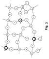
- Fig. 3 is a schematic diagram of the atomic bond state of the SiO 2 -GeO 2 -system thin film shown in a plan view. Fig. 3 shows that the portions indicated by Ge ⁇ are dipoles. The nonlinear optical characteristics originate from the Ge ⁇ portions present in the SiO 2 -GeO 2 -system thin film.
- the operation of applying an electric field to the SiO 2 -GeO 2 -system thin film is referred to as poling.
- the intensity of an electric field used in this case ranges from 50 to 200kv/cm.
- electrodes structured as shown in Figs. 5 to 12 are used.
- the field-applying electrodes are varied with respect to electrode location, whether or not an insulating film is provided and insulating film thickness, because the thickness or the like of the thin film differs with the usage of the deposited the SiO 2 -GeO 2 -system thin film.
- the substrate 12 used is SiO 2 glass measuring 40 ⁇ 40 ⁇ 1mm.
- a SiO 2 -GeO 2 -system thin film 16 is formed by the method mentioned above, and on top of this film, an insulating film 18 of SiO 2 is deposited by vacuum deposition if necessary.
- Ag electrodes 20 for applying an electric field are formed with a thickness of 1 ⁇ m by vacuum deposition.
- the SiO 2 -GeO 2 -system thin film 16 is 2 ⁇ m in thickness, on top of which a SiO 2 insulating film 18 is formed with a thickness of 3 ⁇ m.
- This structure is intended to prevent dielectric breakdown while poling is performed with a high field intensity.
- a SiO 2 -GeO 2 -system thin film 16 with a thickness of 8 ⁇ m is formed on the same SiO 2 substrate 12 as in Fig. 5.
- the Ag electrodes 20 are formed in a similar arrangement to that of Fig. 5.
- the SiO 2 -GeO 2 -system thin film 16 is formed so thick as 8 ⁇ m that dielectric breakdown is less liable to occur, for which reason the SiO 2 insulating film 18 provided in Fig. 5 is omitted here.
- the relation among the substrate 12, the SiO 2 -GeO 2 -system thin film 16 and the insulating film 18 is the same as in Fig. 5, and the thicknesses of the substrate 12 and the SiO 2 -GeO 2 -system thin film 16 are the same as those in Fig. 5.
- both Ag electrodes 20 are disposed between the substrate 12 and the SiO 2 -GeO 2 -system thin film 16. Therefore, the thickness of the SiO 2 insulating film 18 is 2 ⁇ m, thinner by 1 ⁇ m than the 3 ⁇ m in Fig. 5.
- both Ag electrodes 20 are disposed between the SiO 2 insulating film 18 and the SiO 2 -GeO 2 -system thin film 16.
- the SiO 2 insulating film 18 to prevent dielectric breakdown is as thick as 4 ⁇ m.
- the Ag electrodes 20 are disposed between the SiO 2 -GeO 2 -system thin film 16 and the substrate 12.
- the SiO 2 -GeO 2 -system thin film 16 is formed with a large thickness of 4 ⁇ m, thereby obviating the need to provide the SiO 2 insulating film 18.
- the Ag electrodes 20 are placed on the SiO 2 -GeO 2 -system thin film 16.
- a difference from Fig.8 is that in place of the SiO 2 thin film insulating film 18 for dielectric breakdown prevention, another SiO 2 -GeO 2 -system thin film 16 is formed on top of the Ag electrodes 20.
- the SiO 2 -GeO 2 -system thin film 16 on the substrate 12 is 2 ⁇ m thick and the other SiO 2 -GeO 2 -system thin film 16 on the Ag electrodes 20 is 4 ⁇ m thick.
- the Ag electrodes 20 are formed on the SiO 2 -GeO 2 -system thin film 16 and the Ag electrodes 20 are covered with an adhesive 22, such as Araldite.
- the adhesive 22 is used to prevent dielectric breakdown.
- the Ag electrodes 20 are formed on the SiO 2 -GeO 2 -system thin film 16, but a SiO 2 film formed by a sol-gel method is used as the insulating film to prevent dielectric breakdown. Meanwhile, because the SiO 2 film made by the sol-gel method has undergone a dip process, the underside of the substrate 12 is also covered with a SiO 2 film.
- the SiO 2 -GeO 2 -system thin film 16 with electrodes, formed as described, and the substrate 12 are subjected to poling by poling equipment shown in Fig. 13.
- Flourinert 28 which is an inactive insulating oil, is poured into a glass vessel 26 placed on a hot plate 24.
- the Flourinert 28 has a boiling temperature of 215°C and a dielectric strength of 200kv/cm.
- the SiO 2 -GeO 2 -system thin film 16, mounted on the substrate 12 and including electrodes 20, is dipped in the Flourinert 28, and is acted on by an electric field with a predetermined intensity when a voltage is applied across the Ag electrodes 20.
- the Flourinert 28 is heated by the hot plate 24 and its temperature is measured with a thermocouple 30.
- Figs. 14(a),14(b) and 14(c) jointly show the relation between the temperatures of the Flourinert 28 and the field intensity applied to the SiO 2 -GeO 2 -system thin film 16 when poling is performed in the poling equipment shown in Fig. 13.
- Fig. 14(a) shows temperature changes of the Flourinert 28 during poling.
- the Flourinert temperature is changed as follows. The Flourinert temperature is gradually raised from room temperature, and when a predetermined poling temperature is reached, the temperature is held constant for a specified time and is gradually decreased to room temperature.
- Fig. 14(b) shows a pattern of changing the intensity of an electric field applied to the SiO 2 -GeO 2 -system thin film 16 in accordance with temperature changes shown in Fig. 14(a).
- a poling temperature of 200°C is adopted.
- the field intensity is held constant at V1 (50kv/cm), and when the poling temperature is reached, the field intensity is raised to V2 (100kV/cm).
- the field intensity is held constant at V2 for the same specified time as that in Fig. 14(a).
- the field intensity is again lowered to V1 and the Flourinert temperature is gradually decreased.
- the reason why the field intensity is held at a low value while the temperature is low is that if a high field intensity is applied at low temperatures, dielectric breakdown is likely to occur.
- a poling temperature of 250°C is adopted, the field intensity V1 at the first stage is 70kV/cm and the field intensity V2 at the second stage is 120kv/cm.
- the field intensity is continuously raised by degrees from V1 to V2. After this, while the Flourinert temperature is held at the poling temperature, the field intensity is also held at V2. After the lapse of a specified time, the field intensity is decreased continuously from V2 to V1 in step with decreasing temperature.
- the field intensity is held at a relatively low level, and when the temperature of the Flourinert 28 reaches the target poling temperature, a higher field intensity is set.
- a high field intensity can be applied without incurring dielectric breakdown, so that the dipoles can be oriented appropriately.
- the SiO 2 -GeO 2 -system thin film 16 can be made to exhibit sufficiently nonlinear characteristics.
- a specified field intensity is still applied without reducing to zero. This facilitates the orientation of the dipoles to thereby improve the nonlinear optical characteristics.
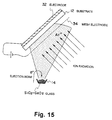
- Fig. 15 shows a modification of the method for manufacturing a nonlinear optical thin film according to the present invention.
- poling is performed simultaneously with forming the SiO 2 -GeO 2 -system thin film 16 on the substrate 12. More specifically, an electrode 32 for poling is formed on the reverse side of the substrate 12 and a mesh electrode 34 is arranged in front of the side of the substrate 12 where the SiO 2 -GeO 2 -system thin film 16 is deposited by electron beam evaporation.
- Fig. 16 is a plan view of the mesh electrode 34. As illustrated in Fig. 16, the mesh electrode 34 has formed therein a specified number of holes 36 to pass therethrough SiO 2 -GeO 2 molecules to be deposited by electron beam evaporation and Ar + ions for ion radiation.
- Fig. 17 shows the principle of a modification of the method for manufacturing a nonlinear optical thin film according to the present invention.
- an oxygen-deficient material is used for the SiO 2 -GeO 2 -system glass to be irradiated with an electron beam to produce the SiO 2 -GeO 2 -system thin film 16.
- This method makes it possible to increase the quantity of produced dipoles origins of the nonlinear optical characteristics. The reason is as follows.
- the oxygen deficiency grows in the SiO 2 -GeO 2 -system thin film, thus yielding a probability of existence of an O 3 -Ge-Ge-O 3 bond as an origin of a dipole, that is, a GeE' center, and increasing the dipole density.
- the O 3 -Ge-Ge-O 3 bond shown in Fig. 17 tends to have the Ge-Ge bond broken by ultraviolet rays or ions and the Ge atoms are liable to be changed into dipoles (GeE' centers).
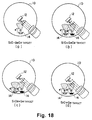
- Fig. 18(a) to 18(d) show examples of oxygen-deficient materials used as targets for electron beam evaporation.
- one hearth liner 14 is provided to hold SiO-GeO 2 and is used as a target.
- two hearth liners 14 are provided, one to hold SiO and the other to hold GeO 2 , and are respectively used as targets of electron radiation.
- Fig. 18(c) also, two hearth liners 14 are provided to hold SiO 2 and Gerespectively and are used as targets of electron radiation.
- Fig. 18(d) too, two hearth liners 14 are provided to hold SiO and Gerespectively and are used as targets of electron radiation.
- SiO, SiO 2 , Ge and GeO 2 may be in a granular or tablet or any other form and may be used independently of each other, or oxygen-deficient tablets of those materials that have been hot-pressed may be used.
- the nonlinear optical characteristics of a SiO 2 -GeO 2 -system thin film thus formed are measured with equipment as illustrated in Fig. 19.
- a sample of a SiO 2 -GeO 2 -system thin film, manufactured by the method for manufacturing a nonlinear optical thin film according to the present invention is irradiated by a laser beam from a Nd:YAG laser, and a wavelength of light coming from the sample is detected by a detector.
- the wavelength of the laser beam is 1064nm, and if the sample has nonlinear optical characteristics, a second harmonic generation (SHG), in other words, light having a wavelength which is 1/2 of the wavelength of the laser beam, is produced.
- SHG second harmonic generation
- the detector measures a wavelength of 532nm.
- the measurement results are shown in Fig. 20.
- the horizontal axis indicates incident angles of the laser beam and the vertical axis indicates the intensities of second harmonic waves.
- the second harmonic waves can be recognized which correspond to the incident angles of the laser beam and it has been clarified that the SiO 2 -GeO 2 system thin film used as the sample have nonlinear optical characteristics.
- nonlinear optical thin films can be formed from glass materials as excellent optical transmission materials. It therefore follows that a nonlinear optical thin film can be formed of the same material as with the core of an optical fiber for transmission, so that loss due to differences in physical properties, such as refractive index and thermal expansion coefficient, can be reduced.
- a SiO 2 -GeO 2 -system glass can be used to realize optical integrated circuits capable of high-speed operations with reduced loss.
- Table 1 shows the evaluation results of characteristics of the SiO 2 -GeO 2 -system thin film according to the present invention compared with those of a ferrodielectric (LiNbO 3 ) and an organic material (MNA: 2-methyl-4-nitroaniline), which have been used as nonlinear thin films.
- the SiO 2 -GeO 2 -system thin film according to the present invention is equivalent to commercially available LiNbO 3 in nonlinear optical characteristics, but is superior to LiNbO 3 and NMA in other characteristics.
- the SiO 2 -GeO 2 -system thin film has no difference in physical properties from optical fiber, which is made of a glass material, and is excellent in connectability with optical fiber.
- a SiO 2 -GeO 2 -system glass, provided as the target, is deposited on a substrate by electron beam evaporation. Because the deposition process is assisted by ion beam assist, dipoles are produced in the deposited SiO 2 -GeO 2 -system thin film. By orienting the dipoles by poling, the deposited thin film can be made into a nonlinear optical thin film with nonlinear optical characteristics.
- the dipoles formed in the SiO 2 -GeO 2 -system thin film can be oriented efficiently.
- the dipoles in the SiO 2 -GeO 2 -system thin film can be formed more easily, thereby improving the nonlinear optical characteristics of the film.
- Figs. 21(a) to 21(c) show the steps of the manufacturing method of a nonlinear optical thin film according to a second embodiment.
- a SiO 2 -GeO 2 -system thin film 16 is deposited on the surface of a substrate 12 by electron beam evaporation by irradiating an electron beam to a SiO 2 -GeO 2 -system glass charged in a hearth liner, not shown.
- this deposition process is assisted by ion beam assist, in which argon ions (Ar + ) are applied.
- the injected energy of argon ions in this case ranges from 1keV to 1MeV.
- ions for use in ion beam assist ions of inert gases such as helium (He) and neon (Ne) may be used in addition to argon.
- the argon ions collide with the molecules of SiO 2 -GeO 2 , thereby forming dipoles (GeE' centers) as the generator of nonlinearity.
- the substrate 12 is heated to about 300°C, for example, the dipoles can be formed more efficiently.
- argon ions can be accumulated on the surface of the SiO 2 -GeO 2 -system thin film 16.
- the substrate 12 has formed on the reverse side thereof a lower electrode 38, which is grounded. Therefore, an electric field is produced between the argon ions (positive ions) accumulated on the SiO 2 -GeO 2 -system thin film 16 and the lower electrode 38, and by this electric field, the dipoles 40 in the SiO 2 -GeO 2 -system thin film 16 are oriented in a fixed direction.
- the SiO 2 -GeO 2 -system thin film 16 is provided with nonlinearity.
- the SiO 2 -GeO 2 -system thin film 16 is formed on the surface of the substrate 12, by changing the injected energy of argon ions for ion beam assist, dipoles as the origins of nonlinearity can be formed and oriented, thus obviating the need to perform an additional poling process after the SiO 2 -GeO 2 -system thin film 16 has been deposited.
- the SiO 2 -GeO 2 -system thin film 16 can be grown to a desired thickness.
- the lower electrode 38 in such a shape as a waveguide pattern, for example, only those dipoles 40 of a specific portion on the substrate 12 can be oriented, and in other words, the dipoles 40 can be easily oriented in a desired pattern. Thus, it becomes easy to produce a waveguide or similar devices.
- pattern control in the orientation process mentioned above can also be performed in such a way as scanning an argon ion beam for ion beam assist in a specified pattern on the deposited film.
- This method obviates the need of photolithography to form the lower electrode 38 in a specified pattern.
- waveguides of different patterns can be produced. Therefore, it becomes easy to produce three-dimensional structures that have quadratic nonlinearity stacked in a number of layers.
- the SiO 2 -GeO 2 -system thin film 16 After the SiO 2 -GeO 2 -system thin film 16 has been formed, by changing the injected energy of argon ions and utilizing the etching effect of ions, for example, it is possible to create fine structures, such as a periodic structure and an optical waveguide in a maskless process.
- the formation and orientation of dipoles can be done in a series of processes by forming a SiO 2 -GeO 2 -system thin film while assisted by ion beam assist and controlling the injected energy of the ions.
Landscapes
- Physics & Mathematics (AREA)
- Nonlinear Science (AREA)
- General Physics & Mathematics (AREA)
- Optics & Photonics (AREA)
- Physical Vapour Deposition (AREA)
- Optical Modulation, Optical Deflection, Nonlinear Optics, Optical Demodulation, Optical Logic Elements (AREA)
- Surface Treatment Of Glass (AREA)
- Optical Integrated Circuits (AREA)
Applications Claiming Priority (4)
| Application Number | Priority Date | Filing Date | Title |
|---|---|---|---|
| JP26812698 | 1998-09-22 | ||
| JP10268126A JP2000098435A (ja) | 1998-09-22 | 1998-09-22 | 非線形光学薄膜の製造方法 |
| JP475099 | 1999-01-11 | ||
| JP11004750A JP2000206578A (ja) | 1999-01-11 | 1999-01-11 | 非線形光学シリカ薄膜の製造方法 |
Publications (2)
| Publication Number | Publication Date |
|---|---|
| EP0989446A2 true EP0989446A2 (de) | 2000-03-29 |
| EP0989446A3 EP0989446A3 (de) | 2001-10-17 |
Family
ID=26338579
Family Applications (1)
| Application Number | Title | Priority Date | Filing Date |
|---|---|---|---|
| EP99117340A Withdrawn EP0989446A3 (de) | 1998-09-22 | 1999-09-03 | Verfahren zur Herstellung einer nichtlinearen optischen Dünnschicht |
Country Status (5)
| Country | Link |
|---|---|
| US (1) | US6358572B1 (de) |
| EP (1) | EP0989446A3 (de) |
| KR (1) | KR100320644B1 (de) |
| AU (1) | AU721595B2 (de) |
| CA (1) | CA2281265C (de) |
Families Citing this family (3)
| Publication number | Priority date | Publication date | Assignee | Title |
|---|---|---|---|---|
| KR100909428B1 (ko) * | 2007-12-08 | 2009-07-28 | 주식회사 유성진공 | 이온빔 보조 전자빔 다층막 증착장치 |
| DE102013207903A1 (de) * | 2013-04-30 | 2014-10-30 | Carl Zeiss Vision International Gmbh | Verfahren zum Beschichten einer Brillenlinse |
| CN111500985B (zh) * | 2020-05-19 | 2022-08-02 | 中国科学院光电技术研究所 | 一种用于低应力全介质光学薄膜的制备方法 |
Citations (2)
| Publication number | Priority date | Publication date | Assignee | Title |
|---|---|---|---|---|
| EP0978754A2 (de) * | 1998-08-07 | 2000-02-09 | Toyota Jidosha Kabushiki Kaisha | Verfahren zur Herstellung einer nichtlinearen optischen Dünnschicht aus Siliziumdioxid und nichtlineares optisches Element aus Siliziumdioxid |
| EP1063557A1 (de) * | 1998-03-12 | 2000-12-27 | Toyota Jidosha Kabushiki Kaisha | Verfahren zur herstellung optisch nichtlinearer dünnfilmwellenleiter sowie optisch nichtlineare dünnfilmwellenleiter |
Family Cites Families (13)
| Publication number | Priority date | Publication date | Assignee | Title |
|---|---|---|---|---|
| JPH0642003B2 (ja) * | 1983-09-20 | 1994-06-01 | オリンパス光学工業株式会社 | 光学部品の反射防止膜とその形成方法 |
| US4906524A (en) * | 1987-05-29 | 1990-03-06 | Orient Watch Co., Ltd. | Surface-coated article and a method for the preparation thereof |
| JPH03202461A (ja) * | 1989-12-29 | 1991-09-04 | Nissin Electric Co Ltd | 高絶縁酸化ケイ素薄膜の形成方法 |
| DE4128547A1 (de) * | 1991-08-28 | 1993-03-04 | Leybold Ag | Verfahren und vorrichtung fuer die herstellung einer entspiegelungsschicht auf linsen |
| CH683776A5 (de) * | 1991-12-05 | 1994-05-13 | Alusuisse Lonza Services Ag | Beschichten einer Substratfläche mit einer Permeationssperre. |
| DE59309018D1 (de) * | 1992-07-02 | 1998-11-05 | Balzers Hochvakuum | Verfahren zur Herstellung einer Metalloxidschicht, Vakuumbehandlungsanlage hierfür sowie mit mindestens einer Metalloxidschicht beschichteter Teil |
| US5462779A (en) * | 1992-10-02 | 1995-10-31 | Consorzio Ce.Te.V. Centro Tecnologie Del Vuoto | Thin film multilayer structure as permeation barrier on plastic film |
| JP2991892B2 (ja) | 1993-05-28 | 1999-12-20 | 信越石英株式会社 | 非線形光学シリカガラスおよびその製造方法 |
| JP2900759B2 (ja) * | 1993-07-20 | 1999-06-02 | 信越化学工業株式会社 | 珪素酸化物蒸着用材料及び蒸着フィルム |
| IT1272248B (it) * | 1994-05-12 | 1997-06-16 | Univ Roma | Fotorivelatore a spettro variabile controllato in tensione, per applicazioni di rivelazione e ricostruzione di immagini bidimensionalia colori |
| US5703710A (en) * | 1994-09-09 | 1997-12-30 | Deacon Research | Method for manipulating optical energy using poled structure |
| JP3119131B2 (ja) * | 1995-08-01 | 2000-12-18 | トヨタ自動車株式会社 | シリコン薄膜の製造方法及びこの方法を用いた太陽電池の製造方法 |
| JP2775416B2 (ja) * | 1995-12-08 | 1998-07-16 | 工業技術院長 | 紫外光照射により体積変化するガラス材料 |
-
1999
- 1999-08-31 CA CA002281265A patent/CA2281265C/en not_active Expired - Fee Related
- 1999-09-03 EP EP99117340A patent/EP0989446A3/de not_active Withdrawn
- 1999-09-11 KR KR1019990038862A patent/KR100320644B1/ko not_active IP Right Cessation
- 1999-09-20 US US09/398,314 patent/US6358572B1/en not_active Expired - Fee Related
- 1999-09-21 AU AU48826/99A patent/AU721595B2/en not_active Ceased
Patent Citations (2)
| Publication number | Priority date | Publication date | Assignee | Title |
|---|---|---|---|---|
| EP1063557A1 (de) * | 1998-03-12 | 2000-12-27 | Toyota Jidosha Kabushiki Kaisha | Verfahren zur herstellung optisch nichtlinearer dünnfilmwellenleiter sowie optisch nichtlineare dünnfilmwellenleiter |
| EP0978754A2 (de) * | 1998-08-07 | 2000-02-09 | Toyota Jidosha Kabushiki Kaisha | Verfahren zur Herstellung einer nichtlinearen optischen Dünnschicht aus Siliziumdioxid und nichtlineares optisches Element aus Siliziumdioxid |
Non-Patent Citations (2)
| Title |
|---|
| SUGIHARA ET AL.: "Thermally poled silicate thin films with large second harmonic generation" OPTICAL SOCIETY OF AMERICA, vol. 15, no. 1, 1 January 1998 (1998-01-01), pages 421-425, XP002174040 * |
| TAKAHASHI M ET AL: "DEFECT FORMATION IN GEO2-SIO2 GLASS BY POLING WITH ARF LASER EXCITATION" APPLIED PHYSICS LETTERS, AMERICAN INSTITUTE OF PHYSICS. NEW YORK, US, vol. 71, no. 8, 25 August 1997 (1997-08-25), pages 993-995, XP000720200 ISSN: 0003-6951 * |
Also Published As
| Publication number | Publication date |
|---|---|
| KR100320644B1 (ko) | 2002-03-13 |
| KR20000023092A (ko) | 2000-04-25 |
| CA2281265A1 (en) | 2000-03-22 |
| US6358572B1 (en) | 2002-03-19 |
| CA2281265C (en) | 2003-12-16 |
| EP0989446A3 (de) | 2001-10-17 |
| AU4882699A (en) | 2000-04-06 |
| AU721595B2 (en) | 2000-07-06 |
Similar Documents
| Publication | Publication Date | Title |
|---|---|---|
| US7132373B2 (en) | Thin metal oxide film and process for producing the same | |
| DE69016538T2 (de) | Verfahren zur Herstellung eines Orientierungsfilms für eine Flüssigkristallanzeigevorrichtung. | |
| Kanetake et al. | Nonlinear optical properties of highly oriented polydiacetylene evaporated films | |
| Burghoff et al. | Structural properties of femtosecond laser-induced modifications in LiNbO 3 | |
| EP0324550B1 (de) | Dünnschichtmusterstruktur | |
| CA2225422C (en) | Laser surface treatment device and method | |
| Rück et al. | Production of buried waveguides in PMMA by high energy ion implantation | |
| EP0989446A2 (de) | Verfahen zur Herstellung eine nichtlineare optische Dünnschicht | |
| Bhat et al. | Irradiation effects on the optical properties of a new NLO mixed borate crystal | |
| US4111520A (en) | Fabrication of optical waveguides | |
| EP1271224A1 (de) | Herstellungsverfahren von Abstandshaltern für Flachbildschirme | |
| CN108681181B (zh) | 显微二阶非线性极化率光学元件的激光辅助热极化设备及方法 | |
| Kameyama et al. | Identification of defects associated with second-order optical nonlinearity in thermally poled high-purity silica glasses | |
| US6627842B1 (en) | Micro-protrusion arrays fabricated by e-beam exposure | |
| Primak | Expansion, crazing and exfoliation of lithium niobate on ion bombardment and comparison results for sapphire | |
| JP2000098435A (ja) | 非線形光学薄膜の製造方法 | |
| KR100441716B1 (ko) | 광비선형 재료 및 그 제조방법 | |
| Moretti et al. | Waveguides fabricated in LiNbO3 by proton implantation | |
| Murr et al. | Scanning electron microscope study of laser‐damaged beryllium thin films | |
| RU2795387C1 (ru) | Способ формирования оптического волновода в кристалле ниобата лития | |
| Buchal et al. | Ion implantation of optical ferroelectrics | |
| Lu et al. | Laser damage threshold of vanadium dioxide film | |
| GB2272434A (en) | Electro-optic modulators and optical frequency convertors in glass waveguides | |
| JP2001013535A (ja) | 非線形光学薄膜の製造方法 | |
| Quagliano et al. | An Investigation of the Chemical and Physical Properties of Pristine, Electrochromically Damaged, and Photochromically Damaged KTiOPO4 (KTP) using Surface Analytical and Optical Spectroscopic Techniques |
Legal Events
| Date | Code | Title | Description |
|---|---|---|---|
| PUAI | Public reference made under article 153(3) epc to a published international application that has entered the european phase |
Free format text: ORIGINAL CODE: 0009012 |
|
| 17P | Request for examination filed |
Effective date: 19990903 |
|
| AK | Designated contracting states |
Kind code of ref document: A2 Designated state(s): AT BE CH CY DE DK ES FI FR GB GR IE IT LI LU MC NL PT SE Kind code of ref document: A2 Designated state(s): DE FR GB IT NL SE |
|
| AX | Request for extension of the european patent |
Free format text: AL;LT;LV;MK;RO;SI |
|
| PUAL | Search report despatched |
Free format text: ORIGINAL CODE: 0009013 |
|
| RIC1 | Information provided on ipc code assigned before grant |
Free format text: 7G 02F 1/35 A, 7G 02F 1/355 B |
|
| AK | Designated contracting states |
Kind code of ref document: A3 Designated state(s): AT BE CH CY DE DK ES FI FR GB GR IE IT LI LU MC NL PT SE |
|
| AX | Request for extension of the european patent |
Free format text: AL;LT;LV;MK;RO;SI |
|
| AKX | Designation fees paid |
Free format text: DE FR GB IT NL SE |
|
| STAA | Information on the status of an ep patent application or granted ep patent |
Free format text: STATUS: THE APPLICATION IS DEEMED TO BE WITHDRAWN |
|
| 18D | Application deemed to be withdrawn |
Effective date: 20060401 |