EP0987826A2 - Circuit de commutation pour un émetteur-récepteur radio - Google Patents
Circuit de commutation pour un émetteur-récepteur radio Download PDFInfo
- Publication number
- EP0987826A2 EP0987826A2 EP99307229A EP99307229A EP0987826A2 EP 0987826 A2 EP0987826 A2 EP 0987826A2 EP 99307229 A EP99307229 A EP 99307229A EP 99307229 A EP99307229 A EP 99307229A EP 0987826 A2 EP0987826 A2 EP 0987826A2
- Authority
- EP
- European Patent Office
- Prior art keywords
- transmitter
- receiver
- antenna
- output signal
- radio transceiver
- Prior art date
- Legal status (The legal status is an assumption and is not a legal conclusion. Google has not performed a legal analysis and makes no representation as to the accuracy of the status listed.)
- Withdrawn
Links
Images

Classifications
-
- H—ELECTRICITY
- H04—ELECTRIC COMMUNICATION TECHNIQUE
- H04B—TRANSMISSION
- H04B1/00—Details of transmission systems, not covered by a single one of groups H04B3/00 - H04B13/00; Details of transmission systems not characterised by the medium used for transmission
- H04B1/38—Transceivers, i.e. devices in which transmitter and receiver form a structural unit and in which at least one part is used for functions of transmitting and receiving
- H04B1/40—Circuits
- H04B1/44—Transmit/receive switching
- H04B1/48—Transmit/receive switching in circuits for connecting transmitter and receiver to a common transmission path, e.g. by energy of transmitter
Definitions
- the invention is generally related to radio transceiver circuits and particularly but not exclusively to pin diode switches used for switching radio transceivers.
- Known radio transceiver circuits with a receiver and a transmitter usually use one common antenna for transmitting and receiving radio signals.
- a switch connects either the input line of the receiver or the output line of the transmitter to the antenna.
- This switch can be a single pole double throw type and is required to isolate the transmitter from the receiver in receive mode and to isolate the receiver from the transmitter in transmit mode. In its off mode it also provides a high impedance for matching. Due to its functions it is referred to as a transmit/receive switch or T/R switch.
- GaAs FET switches which are readily commercially available but are expensive and relatively large. They generally require two control lines to provide the bias voltages for tuming on the transistors.
- a PIN diode switch presents a high impedance to RF frequencies unless a DC bias current is present. When a DC bias current is passed through the diode, the diode is turned on and provides a low resistance RF path between anode and cathode of the diode.
- the PIN diodes are typically coupled together with their cathodes. They are selectively biased by a bias current provided by a switchable power supply. If the power supply for one PIN diode is turned on a bias current flows through the pin diode and if this is e.g. the PIN diode in the receiver path a signal received by the antenna passes the PIN diode, which is now in its conductive state and enters the receiver input stage. The PIN diode in the transmitter path, which is not biased during receive mode, isolates the antenna from the transmitter output stage at the same time.
- blocking capacitors are necessary to isolate the transmitter, the receiver and the antenna from the DC bias current.
- At least three RF chokes are needed for blocking the RF frequency signal from the common ground of the transceiver and from the power supply.
- PIN diode switches One problem with PIN diode switches is that the isolation of the PIN diode switch may not be high enough when the PIN diode is not biased to repress the transmitted signal from the receiver input. Therefore it might be necessary to provide a negative bias current for the PIN diode in the receive path, but providing a negative voltage is also undesirable.
- radio transceiver circuit comprising an antenna, a transmitter, a receiver, an antenna switching circuit for selectively connecting the transmitter and the receiver to the antenna, and a power source for both the transmitter and the receiver, the antenna switching circuit having two semiconductor elements, each having a conductive electrical state and a substantially non-conductive electrical state, one of the semiconductor elements being coupled between the antenna and the transmitter, the other of semiconductor elements being coupled between the antenna and the receiver, whereby the power source is operable to provide the current for powering the transmitter during operation of the transmitter and the receiver during operation of the receiver, current being sought by the transmitter setting the one semiconductor element to its conductive electrical state, current being sought by the receiver setting the other semiconductor element to its conductive electrical state thereby selectively coupling the receiver and the transmitter to the antenna.
- the semiconductive elements are preferably PIN diodes.
- the power supply (Vcc) for biasing the PIN diodes and supplying the transmitter and receiver with the needed biasing current is advantageously connected to the circuit node where the antenna is connected to the anodes or cathodes (dependent on the sign of the power supply) of the PIN diodes through a choke.
- the choke which is coupled between the power source and the antenna is having a high impedance for RF signals and a low impedance for DC signals in order to provide the DC current for the PIN diodes, the receiver and transmitter circuit and block the RF signal from the power supply.
- the choke can be one of the matching components for the antenna which is used for providing the correct impedance matching for the antenna.
- the transmitter and the receiver circuit include open collector output stages.
- the power amplifier of the transmitter contains an open collector output stage and the bias current is feeding directly into the output of the power amplifier for biasing. This bias current is also used for biasing the PIN diode in the path between the antenna and the transmitter. This power amplifier could be advantageously the last power amplifier stage of the transmitter.
- components of the receiver for example a mixer of the receiver, could contain an open collector output stage and the mixer of the receiver requires the current which is used for biasing the PIN diode which is coupled between the antenna and the receiver.
- the transmitter is operated with a balanced output signal.
- the power amplifier of the transmitter produces a first output signal with the half of the amplitude required for transmission and a second output signal also with the half of the amplitude required for transmission which is inverted to the first output signal.
- the second output signal is phase shifted by a phase shifting element, which can be for example a balun, and added to the first output signal to provide the required transmitter output signal.
- the summation signal of the inverted and non-inverted transmitter output signal is then connected to the PIN diode in the transmitter path and the output signal of the transmitter is connected to the antenna during operation of the transmitter.
- a method of operating a semiconductor element switch of a transceiver for selectively coupling an antenna to the transmitter and receiver, the semiconductor element switch having two semiconductor elements each having a conductive electrical state and a substantially non-conductive electrical state, the current sought from a power source by a transmitter of the transceiver during operation of the transmitter or by a receiver of the transceiver during operation of the receiver being used to set the respective semiconductor element into a conductive electrical state thereby connecting the antenna to the transmitter during operation of the transmitter and to the receiver during operation of the receiver.
- a radio transceiver circuit comprising a transmitter having means for providing a balanced output signal with an inverted output signal and a non inverted output signal , and a receiver, the inverted transmitter output signal is phase shifted by a first phase shifting element and a second phase shifting element and combined with the non inverted output signal to provide an output signal, the first and second phase shifting elements are arranged such that the combined signal of the inverted and non inverted transmitter output signals is substantially zero at a node where the two phase shifting elements are coupled together, and said receiver is coupled to said node.
- phase shifting elements i.e. baluns
- the phase shifting elements are arranged in a way that the sum of the signals of the inverted and non-inverted transmitter output signal becomes substantially zero at the connection point of the phase shifting elements.
- the input line of the receiver is connected to the connection point of the two phase shifting element.
- two PIN diodes for de-coupling the transmitter circuitry from the receiver circuitry are located within the inverted and non inverted output signal path of the transmitter providing a balanced output signal. While the transmitter is not operating these PIN diodes are in their non-conductive electrical state because the transmitter does not require a current for operation which bias the PIN diodes.
- This invention facilitates a receive path from the antenna to the receiver without using any kind of switching or de-coupling element for de-coupling the receiver path from the antenna path.
- a transceiver circuit according to the prior art with a transmitter 1 and a receiver 2.
- Transmitter 1 and receiver 2 are coupled to a circuit node A via DC-blocking capacitors 3 and 4 and PIN diodes 15 and 16 having their cathodes coupled together.
- Antenna 21 is connected to the circuit node A via a DC blocking capacitor 22.
- the switch 19 is closed and a biasing current I B is feeding from the power source 24a through switch 19, choke 17, PIN diode 15 and choke 23 to ground. This way the diode 15 is set into its conductive electrical state and the signal to be transmitted can pass from transmitter 1 through PIN Diode 15 through capacitor 22 to the antenna 21.
- Switches 19 and 20 may be controlled by a microprocessor which also controls other operations of the transceiver.
- receive mode switch 20 In receive mode switch 20 is closed and the PIN diode 16 is biased this way. Switch 19 is opened to set pin diode 15 in a non-conductive electrical state. A signal received by antenna 21 passes through capacitor 22 and PIN diode 16, DC blocking capacitor 4 to the input stage of receiver 2.
- the main disadvantage for this kind of transceiver switching circuit is that the current I B is only needed for biasing the PIN diodes 15 and 16 in transmit and receive mode. In each case an external current must be supplied by the control circuitry to bias the PIN diodes. Furthermore the blocking capacitors 3 and 4 are necessary to isolate the transmitter output stage and the receiver input stage from the DC bias current. Another disadvantage is that two control lines containing the switches 19 and 20 and the chokes 17 and 18 are required.
- the radio transceiver circuit basically comprises an antenna 21, a transmitter 11, a receiver 12, an antenna switching circuit connecting the transmitter 11 and the receiver 12 to the antenna 21 and a power source Vcc 24.
- the antenna switching circuit is a construction of two semiconductor elements, namely PIN diodes 15 and 16, having a conductive electrical state and a substantially non-conductive electrical state coupled together with their anodes which are connected to the circuit node A and by this to the antenna 21.
- Antenna 21 is coupled through DC blocking capacitor 22 to circuit node A.
- the power source Vcc 24 is coupled through the RF blocking choke 23 to the circuit node A.
- the currents I BTX , I BRX sought from the power source by means of receiver 12 or transmitter 11 during operation of said means are directed through the respective PIN diodes (15,16) which are set to their conductive electrical state by this currents and thereby the transmitter is connected to the antenna when the transmitter is in operation and the receiver is coupled to the antenna when the receiver is in operation.
- the current I BTX biasing the PIN diode 15 during transmit mode also enters the output of the final power amplifier 18.
- Power Amplifier 18 contains an open collector output stage which is known to persons skilled in the art.
- the current I BTX is feeding into the output of the amplifier 18 for biasing the transmitter 14 during transmit mode.
- PIN diode 15 is turned on automatically by the bias current I BTX of the power amplifier 18.
- the bias current I BTX is feeding from the power source Vcc 24 through choke 23 and PIN diode 15 to the power amplifier 18 and through line 51 to ground.
- the power amplifier 17 uses an own power source 54 but it has to be understood if for example the bias current sought by the power amplifier 18 is not high enough for biasing PIN diode 15 the bias currents of power amplifiers 17 and 18 can be coupled together for biasing PIN diode 15. Furthermore it is possible only to use the bias current sought by power amplifier 17 that may be sufficient to bias PIN diode 15 and set it into its electrically conductive state.
- the bias currents sought by any parts of transmitter 11 can be chosen such that a minimum but sufficient current I BTX is fed through the PIN diode for biasing.
- the receiver 12 of Fig. 2 contains basically a Low Noise Amplifier (LNA) 13 and a mixer 14. During operation of receiver 12 the mixer 14 and the LNA 13 require bias currents for their open collector output stages. In this case the bias current of the mixer 14 is used to bias also the PIN diode 16.
- the bias current I BTX is feeding from power source Vcc 24 through choke 23, pin diode 16 and RF choke 27 to the mixer 14 for biasing the mixer 14 and through connection line 53 to ground.
- LNA 13 is connected to a supplementary power source 55 for biasing.
- the receiver part it may be possible to use the biasing current of the LNA 13 if it is high enough for biasing the PIN diode 16 or to couple together the bias currents of mixer 14 and LNA 13 for biasing the PIN diode 16. Also bias currents used by any other stages of the receiver could be used for biasing PIN diode 16. Also the mixer 14 in this case contains an open collector output stage and the current I BRX is used for biasing.
- the signal leaving the LNA 13 is then down-converted by the mixer 14 to an intermediate frequency. Further receiver stages may be necessary to amplify and down-convert the received signal.
- the signal leaving receiver 12 is further processed and could be finally fed to a loudspeaker for speech transmission or to a microprocessor for data transmission.
- a DC blocking capacitor 28 is used to block the bias current I BRX from the input stage of LNA 13.
- the PIN diode bias currents are now regulated by the open collector output stages and so they are less susceptible to noise which could otherwise disturb the system.
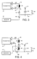
- Fig. 3 shows a variant of the transceiver circuit presented in Fig. 2 which is substantially the same except the output stage of transmitter 31.
- Transmitter 31 contains a balanced output signal. This balanced output signal is characterised by an non-inverted output signal TX and an inverted output signal TX . Both output signals have about the half amplitude of the final output signal which is fed to the antenna 21.
- the inverted output signal TX is phase shifted by a delay line 33.
- Delay line 33 can be for example a balancing transformer which is known as a balun to persons skilled in the art.
- Balun 33 shifts the inverted output signal for Z degrees.
- Z is 180 in general but for systems where the output frequency varies between two frequencies, known as frequency bands, the balun is designed in a way that a ideal 180 degree phase shift is obtained for a frequency in the middle of this band and an acceptable phase shift is obtained for the lowest and the highest possible frequency of the output signal.
- the balun is designed for 180 degree phase shift at 2.45 GHz.
- the inverted and non-inverted output signal are combined at the cathode of PIN diode 15.
- the optimal output signal is reached at 2.45 GHz but also for transmit frequencies of 2.4 and 2.5 GHz a loss of about 1.5 dB at this borders is acceptable.
- power amplifiers for the inverted output signal and for the non-inverted output signal require currents for biasing their open collector output stages.
- This current is sought from the power source 24 through choke 23 and PIN diode 15 and is then divided into the inverted and non-inverted signal path, i.e. the currents I BTX and I BTX .
- the sum of these two currents is used for biasing PIN diode 15 and set it to its conductive electrical state.
- receiver 32 is the same as the operation of receiver 12 in Fig. 1.
- Receiver 32 might also be a receiver with a balanced input signal with means for phase shifting one half of the incoming signal.
- circuit of Fig. 3 uses the advantages of the invention as they are presented in Fig. 2, i.e. the currents for biasing transmitter and receiver stages are used for biasing the respective PIN diodes in the transmitter and receiver path to the antenna.
- the circuitry as it is shown in Figure 4 also takes advantage of the fact that a current sought by the transmitter for biasing the open collector output stages is used for biasing the PIN diode 15a and 15b but for obtaining a good isolation of the input stage of receiver 32 to the transmitter output signal another approach is disclosed.
- the output signal of the transmitter 31 is balanced like it is presented with reference to Fig. 3 and the accompanying description and consists of an inverted and non-inverted output signal.
- two baluns 45 and 46 are used for phase shifting.
- the first balun 45 shifts the inverted transmitter output signal TX for X degrees.
- X should be substantially around 90 degree ((/4).
- Balun 46 shifts the inverted output signal again for 90 degrees (phase shift Y°), in order to obtain a 180 degree phase shift as described above. Both output signals are combined at circuit node A and the obtained total transmitter output signal is send out through antenna 21.
- baluns 45 and 46 The advantage of this kind of phase shifting with baluns 45 and 46 is, that the non-inverted output signal TX of transmitter 31 also passes the balun 46 where it is (/4 shifted and meets the inverted and (/4 phase shifted output signal TX at connection node B.
- connection node B of the two signals TX and TX leads to a signal with no amplitude at this node (Zero point). It could be possible that also other parts of the switching circuit have got a phase shifting effect, therefore the baluns 45 and 46 have to be dimensioned in a way that these effects are extinguished and the transmitter signal is substantially zero in connection node B.
- the input stage of receiver 42 is connected to connection node B. During transmitter operation no signal from the transmitter path enters the receiver path, this way the receiver is ideally isolated from the transmitter path even if it is directly connected to it at connection node B.
- a received signal is fed through antenna 21, capacitor 22, balun 46 to the input stage of receiver 32.
- This signal is phase shifted also by balun 46 but this does not have any further technical effect on the received radio frequency signal.
- the PIN diodes 15a and 15b de-couple transmitter 31 from the received signal during receive mode. While transmitter 31 is operating the currents I BTX and I BTX for biasing the power amplifier are also fed through PIN diodes 15a and 15b for tuming them on and the transmit signals can pass to antenna 21. During receiver operation, i.e. the transmitter is turned off, the PIN diodes 15a, 15 b are not biased and therefore in their non conductive electrical state and the received signal passing from the antenna 21 to the receiver input stage does not enter the transmitter output stages.
- the receiver may also obtain its biasing current for one or more open collector output stages from power source 24 but this is not necessary with regard to the invention because the biasing current is not needed for biasing any PIN diode in the receiver path.
- PIN diode 15a which de-couples the inverted transmitter output stage during receive mode, is positioned between balun 45 and connection node B with the cathode connected to balun 45 and the anode coupled to the circuit node B.
- PIN diode 15b which de-couples the non-inverted transmitter output stage during receive mode, is positioned between circuit node A and the non-inverted transmitter output stage.
- the power source Vcc 24 together with RF blocking choke 23 can be directly connected to connection node B or any other usable point where it supplies the transmitter with current and bias the PIN diodes (15a,15b) while the transmitter 41 is operating.
- the present invention may include any novel feature or combination of features disclosed herein either explicitly or implicitly or any generalisation thereof irrespective of whether or not it relates to the presently claimed invention or mitigates any or all of the problems addressed.
- any novel feature or combination of features disclosed herein either explicitly or implicitly or any generalisation thereof irrespective of whether or not it relates to the presently claimed invention or mitigates any or all of the problems addressed.
Landscapes
- Engineering & Computer Science (AREA)
- Computer Networks & Wireless Communication (AREA)
- Signal Processing (AREA)
- Transceivers (AREA)
Applications Claiming Priority (2)
| Application Number | Priority Date | Filing Date | Title |
|---|---|---|---|
| GB9820469A GB2341755A (en) | 1998-09-18 | 1998-09-18 | Radio transceiver switching circuit |
| GB9820469 | 1998-09-18 |
Publications (2)
| Publication Number | Publication Date |
|---|---|
| EP0987826A2 true EP0987826A2 (fr) | 2000-03-22 |
| EP0987826A3 EP0987826A3 (fr) | 2004-02-25 |
Family
ID=10839156
Family Applications (1)
| Application Number | Title | Priority Date | Filing Date |
|---|---|---|---|
| EP99307229A Withdrawn EP0987826A3 (fr) | 1998-09-18 | 1999-09-13 | Circuit de commutation pour un émetteur-récepteur radio |
Country Status (3)
| Country | Link |
|---|---|
| US (1) | US6459885B1 (fr) |
| EP (1) | EP0987826A3 (fr) |
| GB (1) | GB2341755A (fr) |
Cited By (1)
| Publication number | Priority date | Publication date | Assignee | Title |
|---|---|---|---|---|
| GB2389485A (en) * | 2002-06-07 | 2003-12-10 | Sony Uk Ltd | Pre-amplification transmit isolation switch in a mobile transceiver front end |
Families Citing this family (15)
| Publication number | Priority date | Publication date | Assignee | Title |
|---|---|---|---|---|
| US6917789B1 (en) * | 1999-10-21 | 2005-07-12 | Broadcom Corporation | Adaptive radio transceiver with an antenna matching circuit |
| DE10053205B4 (de) * | 2000-10-26 | 2017-04-13 | Epcos Ag | Kombinierte Frontendschaltung für drahtlose Übertragungssysteme |
| GB2374203A (en) * | 2001-04-06 | 2002-10-09 | Alexander Dodd | Transmit / receive antenna system with higher receive gain |
| JP2003133972A (ja) * | 2001-10-29 | 2003-05-09 | Fujitsu Ltd | 無線送信機を有する電子装置 |
| US6927647B2 (en) * | 2002-06-11 | 2005-08-09 | Ernesto G. Starri | Two channels, high speed, RF switch |
| JP4029779B2 (ja) * | 2003-06-05 | 2008-01-09 | 株式会社村田製作所 | 高周波モジュールおよび通信装置 |
| US20050255812A1 (en) * | 2004-05-17 | 2005-11-17 | Samsung Electronics Co., Ltd. | RF front-end apparatus in a TDD wireless communication system |
| JP2006050054A (ja) * | 2004-08-02 | 2006-02-16 | Matsushita Electric Ind Co Ltd | 無線電話装置およびその消費電流制御方法 |
| JP2009528781A (ja) * | 2006-02-28 | 2009-08-06 | ルネサンス・ワイヤレス | Rfトランシーバスイッチングシステム |
| KR100965655B1 (ko) * | 2006-03-06 | 2010-06-23 | 삼성전자주식회사 | 통신 시스템에서 신호 송수신 방법 |
| US8099062B1 (en) * | 2008-04-24 | 2012-01-17 | Qualcomm Atheros, Inc. | CMOS transceiver analog front end having a combined power amplifier and low noise amplifier |
| TW201432999A (zh) * | 2012-10-31 | 2014-08-16 | Galtronics Corp Ltd | 寬頻鞭狀天線 |
| US9306613B2 (en) * | 2013-01-10 | 2016-04-05 | Google Technology Holdings LLC | Variable antenna match linearity |
| US9564892B2 (en) | 2015-03-06 | 2017-02-07 | Skyworks Solutions, Inc. | Apparatus and methods for radio frequency PIN diode switches |
| US11152969B2 (en) * | 2018-11-21 | 2021-10-19 | Panasonic Avionics Corporation | Tile based satellite payload systems and associated methods thereof |
Citations (4)
| Publication number | Priority date | Publication date | Assignee | Title |
|---|---|---|---|---|
| US4520476A (en) * | 1982-12-13 | 1985-05-28 | Rockwell International Corporation | Apparatus for enabling the duplex operation of a transmitter and receiver |
| US4637065A (en) * | 1984-05-07 | 1987-01-13 | Motorola, Inc. | Broadband solid state antenna switch |
| US4979232A (en) * | 1989-08-14 | 1990-12-18 | Harris Corporation | Self-biasing solid-state T/R switch |
| JPH1028081A (ja) * | 1996-07-10 | 1998-01-27 | Sony Corp | 平衡伝送装置及び平衡調整回路 |
Family Cites Families (5)
| Publication number | Priority date | Publication date | Assignee | Title |
|---|---|---|---|---|
| US4525863A (en) * | 1983-10-19 | 1985-06-25 | Gte Laboratories Incorporated | Solid state transmit/receive switch |
| GB2273423B (en) * | 1992-12-10 | 1997-04-16 | Motorola Gmbh | An antenna switching circuit and method for operating an antenna switch |
| JPH077449A (ja) * | 1993-06-17 | 1995-01-10 | Oki Electric Ind Co Ltd | アンテナ切り替えスイッチ |
| US5789995A (en) * | 1996-09-20 | 1998-08-04 | Motorola, Inc. | Low loss electronic radio frequency switch |
| US6122488A (en) * | 1998-03-05 | 2000-09-19 | Motorola, Inc. | Method and apparatus for increasing an output impedance of a transmit amplifier during receive mode of a two-way communication unit |
-
1998
- 1998-09-18 GB GB9820469A patent/GB2341755A/en not_active Withdrawn
-
1999
- 1999-09-13 EP EP99307229A patent/EP0987826A3/fr not_active Withdrawn
- 1999-09-17 US US09/397,854 patent/US6459885B1/en not_active Expired - Fee Related
Patent Citations (4)
| Publication number | Priority date | Publication date | Assignee | Title |
|---|---|---|---|---|
| US4520476A (en) * | 1982-12-13 | 1985-05-28 | Rockwell International Corporation | Apparatus for enabling the duplex operation of a transmitter and receiver |
| US4637065A (en) * | 1984-05-07 | 1987-01-13 | Motorola, Inc. | Broadband solid state antenna switch |
| US4979232A (en) * | 1989-08-14 | 1990-12-18 | Harris Corporation | Self-biasing solid-state T/R switch |
| JPH1028081A (ja) * | 1996-07-10 | 1998-01-27 | Sony Corp | 平衡伝送装置及び平衡調整回路 |
Non-Patent Citations (1)
| Title |
|---|
| PATENT ABSTRACTS OF JAPAN vol. 1998, no. 05, 30 April 1998 (1998-04-30) & JP 10 028081 A (SONY CORP), 27 January 1998 (1998-01-27) * |
Cited By (1)
| Publication number | Priority date | Publication date | Assignee | Title |
|---|---|---|---|---|
| GB2389485A (en) * | 2002-06-07 | 2003-12-10 | Sony Uk Ltd | Pre-amplification transmit isolation switch in a mobile transceiver front end |
Also Published As
| Publication number | Publication date |
|---|---|
| GB9820469D0 (en) | 1998-11-11 |
| US6459885B1 (en) | 2002-10-01 |
| GB2341755A8 (en) | 2000-07-10 |
| EP0987826A3 (fr) | 2004-02-25 |
| GB2341755A (en) | 2000-03-22 |
Similar Documents
| Publication | Publication Date | Title |
|---|---|---|
| US6459885B1 (en) | Radio transceiver switching circuit | |
| US7428230B2 (en) | Time-division-duplexing type power amplification module | |
| EP0741463B1 (fr) | Radio émetteur-récepteur semi-duplex produisant une faible atténuation du signal d'émetteur | |
| US6072993A (en) | Portable radio transceiver with diplexer-switch circuit for dual frequency band operation | |
| US8022786B2 (en) | Front-end circuit of the wireless transceiver | |
| US5784687A (en) | Transmitting-receiving circuit for radiocommunication apparatus, semiconductor integrated circuit device including the circuit, and radiocommunication apparatus including the same | |
| US5822684A (en) | Antenna switching circuit and wireless communication system | |
| KR100844398B1 (ko) | 다중 레벨 전력 증폭기 | |
| KR100671651B1 (ko) | 이중 대역 이동 전화의 고조파 억제 장치 및 방법 | |
| US7197284B2 (en) | Antenna switches including field effect transistors | |
| US6667723B2 (en) | System and method for a GPS enabled antenna | |
| US6510310B1 (en) | Dual mode phone architecture utilizing a single transmit-receive switch | |
| US20060009164A1 (en) | Radio frequency switching circuit | |
| EP1402651B1 (fr) | Systeme permettant d'obtenir une antenne gps | |
| US20050107043A1 (en) | Integration of diversity switch in combination with a T/R switch for a radio transceiver on a single chip | |
| US6487395B1 (en) | Radio frequency electronic switch | |
| US6950634B2 (en) | Transceiver circuit arrangement and method | |
| US6351628B1 (en) | Antenna switching circuit | |
| CN1898877B (zh) | 用于vco中不相等功率分配的定向耦合器 | |
| JPWO2009013813A1 (ja) | 送受信回路 | |
| US6693677B1 (en) | Apparatus for commonly using antenna for call signal and television broadcasting signal in radio communication terminal | |
| EP1738478B1 (fr) | Circuit efficace de commutation d'antenne a plusieurs bandes | |
| EP1649476A2 (fr) | Interrupteur bipolaire unidirectionnel radiofrequence | |
| US7643814B2 (en) | Reception arrangement with preamplifier circuit | |
| JPH1093470A (ja) | アンテナ共用回路 |
Legal Events
| Date | Code | Title | Description |
|---|---|---|---|
| PUAI | Public reference made under article 153(3) epc to a published international application that has entered the european phase |
Free format text: ORIGINAL CODE: 0009012 |
|
| AK | Designated contracting states |
Kind code of ref document: A2 Designated state(s): AT BE CH CY DE DK ES FI FR GB GR IE IT LI LU MC NL PT SE |
|
| AX | Request for extension of the european patent |
Free format text: AL;LT;LV;MK;RO;SI |
|
| RIN1 | Information on inventor provided before grant (corrected) |
Inventor name: BURGESS, PAUL |
|
| RAP1 | Party data changed (applicant data changed or rights of an application transferred) |
Owner name: NOKIA CORPORATION |
|
| 17P | Request for examination filed |
Effective date: 20030912 |
|
| PUAL | Search report despatched |
Free format text: ORIGINAL CODE: 0009013 |
|
| AK | Designated contracting states |
Kind code of ref document: A3 Designated state(s): AT BE CH CY DE DK ES FI FR GB GR IE IT LI LU MC NL PT SE |
|
| AX | Request for extension of the european patent |
Extension state: AL LT LV MK RO SI |
|
| 17Q | First examination report despatched |
Effective date: 20040706 |
|
| AKX | Designation fees paid |
Designated state(s): DE FR GB NL |
|
| STAA | Information on the status of an ep patent application or granted ep patent |
Free format text: STATUS: THE APPLICATION IS DEEMED TO BE WITHDRAWN |
|
| 18D | Application deemed to be withdrawn |
Effective date: 20041117 |