EP0987652A2 - IC card and its manufacturing method - Google Patents
IC card and its manufacturing method Download PDFInfo
- Publication number
- EP0987652A2 EP0987652A2 EP99307396A EP99307396A EP0987652A2 EP 0987652 A2 EP0987652 A2 EP 0987652A2 EP 99307396 A EP99307396 A EP 99307396A EP 99307396 A EP99307396 A EP 99307396A EP 0987652 A2 EP0987652 A2 EP 0987652A2
- Authority
- EP
- European Patent Office
- Prior art keywords
- chip
- card
- mirror surface
- etching
- dicing
- Prior art date
- Legal status (The legal status is an assumption and is not a legal conclusion. Google has not performed a legal analysis and makes no representation as to the accuracy of the status listed.)
- Granted
Links
Images


Classifications
-
- G—PHYSICS
- G06—COMPUTING OR CALCULATING; COUNTING
- G06K—GRAPHICAL DATA READING; PRESENTATION OF DATA; RECORD CARRIERS; HANDLING RECORD CARRIERS
- G06K19/00—Record carriers for use with machines and with at least a part designed to carry digital markings
- G06K19/06—Record carriers for use with machines and with at least a part designed to carry digital markings characterised by the kind of the digital marking, e.g. shape, nature, code
- G06K19/067—Record carriers with conductive marks, printed circuits or semiconductor circuit elements, e.g. credit or identity cards also with resonating or responding marks without active components
- G06K19/07—Record carriers with conductive marks, printed circuits or semiconductor circuit elements, e.g. credit or identity cards also with resonating or responding marks without active components with integrated circuit chips
- G06K19/077—Constructional details, e.g. mounting of circuits in the carrier
- G06K19/0772—Physical layout of the record carrier
- G06K19/07728—Physical layout of the record carrier the record carrier comprising means for protection against impact or bending, e.g. protective shells or stress-absorbing layers around the integrated circuit
-
- G—PHYSICS
- G06—COMPUTING OR CALCULATING; COUNTING
- G06K—GRAPHICAL DATA READING; PRESENTATION OF DATA; RECORD CARRIERS; HANDLING RECORD CARRIERS
- G06K19/00—Record carriers for use with machines and with at least a part designed to carry digital markings
- G06K19/06—Record carriers for use with machines and with at least a part designed to carry digital markings characterised by the kind of the digital marking, e.g. shape, nature, code
- G06K19/067—Record carriers with conductive marks, printed circuits or semiconductor circuit elements, e.g. credit or identity cards also with resonating or responding marks without active components
- G06K19/07—Record carriers with conductive marks, printed circuits or semiconductor circuit elements, e.g. credit or identity cards also with resonating or responding marks without active components with integrated circuit chips
- G06K19/077—Constructional details, e.g. mounting of circuits in the carrier
Definitions
- IC cards Integrated Circuit cards
- IC cards can have the following features.
- a card is put in a purse, a card case or carried loose whether it is an IC card or a magnetic card, so the IC card is required to satisfy at least the same specifications as magnetic card, such as the following.
- the IC card has the IC chip, therefore, the IC card has a possibility of damage of the IC chip by transformation such as flexing, bending or otherwise distorting the IC card.
- the following is important in order to improve the reliability of the IC card against transformation.
- Prior art 1 discloses an IC card structure in which the IC chip suppresses transformation by holding and reinforcing the IC chip with a metal plate.
- the IC chip itself should be thin and that defects of the IC chip surface are decreased so that it is hard to destroy it by transformation.
- the bending transformation of the IC chip and the stress of the IC chip surface are proportional to the thickness of the IC chip.
- Silicon used as a material of the IC chip. Silicon is a brittle material. The IC chip is destroyed by mirror surface defects. So, it is desirable to decrease defects of the chip mirror surface.
- Prior art 2 discloses the manufacturing method of removing micro-cracks on the mirror surface of the IC chip by an etching process.
- the Japanese patent Laid-open print No. 4-62921 (prior art 3) uses a plasma etching machine and discloses a removal of the reaction secondary product by two step etching.
- the Japanese patent Laid-open print No. 6-232255 discloses dicing a wafer from the mirror surface of the chip to prevent the chipping that occurs in the mirror surface of the chip.
- the IC chip after dicing is thin, and the area is small. Therefore, it is difficult to selectively etch only the mirror surface of the IC chip by plasma etching, etc. because of the problem of productivity and the transfer.
- isotropical chemical etching, etc. the device surface of the IC chip is eroded by etching.
- the purpose of the present invention is to provide an IC card which has high reliability against transformation by external force.
- an IC card which comprises at least one IC chip having a device surface where a circuit is formed, a mirror surface which is located in the opposite side the device surface, and side surfaces which substantially perpendicular surfaces for the device surface, base plates which are softer than said IC chip, said base plates are laminated and formed external form of the IC card, said IC chip is located inside the IC card; and said mirror surface and said side surfaces are etched, whereby sharp regions of chippings formed said mirror surface and said side surfaces are substantially removed and cracks in the IC chip is prevented.
- a method of manufacturing said IC card external form is formed by laminated base plates which are softer than an IC chip and at least one IC chip is located inside the IC card, which comprises forming a circuit on a wafer device surface, applying a protection agent to said wafer device surface, dicing said wafer to made several IC chips, etching said IC chips, and removing said protection agent, whereby said etching etched a mirror surface of said IC chip which is located in the opposite side the device surface, and side surfaces of said IC chip, which substantially perpendicular surfaces for the device surface and sharp region of chipping formed said mirror surface and said side surfaces are substantially removed and a crack in the IC chip is prevented.
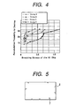
- the inventors determined a breaking stress on the mirror surface and the device surface of the IC chip by a 3-point bending test.
- the test result was analysed by accumulative probability to destroy against breaking stress (Fig. 3).
- Fig. 3(A) illustrates the breaking stress of the mirror surface of the IC chip.
- Fig. 3(B) illustrates the breaking stress of the device surface of the IC chip.
- the breaking stress on the mirror surface of the IC chip is smaller than breaking stress on the device surface of the IC chip and the dispersion of breaking stress also enlarges.
- Fig. 5 the type of defects on the mirror surface after dicing the IC chip are shown.
- the circumference part of the chip has many inherent flaws. This is chipping caused on the mirror surface of the IC card by the process of dicing. From this, the destruction strength of the IC chip declines by the chipping that arises on the mirror surface side by dicing of the manufacturing process of the IC chip.
- Fig. 1 is the sectional view of the IC card that is example of the present invention.
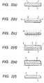
- Fig. 2(a) to (f) show part of the manufacturing process of the IC chip that is the example of the present invention.
- Fig. 3(a) and (b) illustrate relationship found by the inventors between the accumulative probability to destroy and the breaking stress of the IC chip that is used for a conventional IC card.
- Fig. 4 illustrates a relationship found by the inventors between accumulative probability to destroy and the breaking stress by dicing condition of the IC chip that is used for a conventional IC card.
- Fig. 5 represents the state of the mirror surface after dicing of the IC chip that is used for a conventional IC card as found by the inventors.
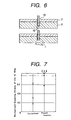
- Fig. 6 represents the generation mechanism of the chipping in the manufacturing process of the IC chip as analysed by the inventors.
- Fig. 7 is the figure that shows the difference between the breaking stresses of the IC chip of the present invention and a conventional IC chip.
- Fig. 1 is a sectional view of the IC card of this example.
- the thickness of the IC card of this example is about 0.46mm.
- Card base material 11 is pasted together by adhesive 12, and IC chip 9 and circuit layer 13 are included.
- IC chip 9 the mirror surface and the side are etched.
- the IC chip being strength is enlarged.
- a protection agent such as epoxy resin is first applied to surface 3 of the device of wafer 1 before mirror surface grinding and dicing as protection agent 2.
- the protection agent does not need to be epoxy resin. It has only to be a material that is not eroded in the etching process (Fig. 2(e)) that is done later. For example, heat curable resin, thermoplastic resin, etc. are fine.
- the purpose of applying the protection agent is that it prevents erosion of the device surface of the IC chip by the etching process (Fig. 2(e)).
- the protection agent is applied before mirror surface grinding and dicing and after the circuit installation. It is contemplated to apply the protection agent after mirror surface grinding.
- the time of the protection agent application is before dicing process, otherwise it is not limited especially.
- the mirror surface grinding process (Fig. 2(b)) is done from the side of the previous mirror surface 4 of the wafer.
- the thickness may be 0.76 - 0.25mm.
- the IC chip needs grinding until the thickness becomes 0.2mm or less.
- the IC chip stored in the IC card likewise with the IC card, is bent by force applied from the outside when carrying and using the IC card. Transformation arises and a stress occurs on the surface of the IC chip.
- the thickness of the IC chip is defined as T
- the Young's modulus of the IC chip is defined as E
- radius of curvature of the IC chip is defined as R.
- the thickness of the IC chip is reduced, the bending stress of the IC chip is reduced for a bending transformation of an IC chip of the same radius of curvature. Therefore, as for the IC chip, it is desirable that it is ground as thin as possible. However, grinding flaws 6 arises in mirror surfaces 5 of wafer 1 at the time of mirror surfaces grinding.
- the IC card of which the thickness is 0.46mm or more.
- the IC chip of which the bending strength is high can be manufactured. Manufacturing of the IC card of high reliability is enabled.
- Dicing process (Fig. 2(c)) of the next ground IC chip is done. Dicing uses a blade of 20 ⁇ m thickness here. The protection agent also is cut with the wafer by dicing process (Fig. 2(c)). There is a fear of the occurrence of chipping 7 in the circumference part of the IC chip by dicing process (Fig. 2(c)). A chipping generation mechanism is shown in Fig. 6. When blade 10 cuts protection agents 2 and wafer 1, the part of wafer that is not cut destroys the part from which wafer was cut as starting point 15. This destruction is called chipping. It is thought that the vibration that is given to wafer 1 by the rotation of blade 10 is the cause of this.
- Fig. 5 shows the chipping that occurs in the IC chip by dicing.
- Chipping 7 comes to the circumference of the IC chip like a notch.
- the depth of chipping 7 is generally from 10 ⁇ m to more than 100 ⁇ m.
- Chipping 7 can reduce the bending strength of the IC chip.
- the method of slowing the transmission speed of the blade 10 in order to reduce generation of this chipping as much as possible has been considered. But this method would increase the time that is needed in dicing process.
- coming of the sharp notch of the chipping 7 tip part is removed in the back etching process (Fig. 2(e)).
- the chip after dicing consists like of Fig. 2(d). Grinding flaw 6 and chipping 7 arise in mirror surface 5 in IC chip 8 after dicing.
- Etching processing is done by chemical etching by the mixture liquid of fluoric acid, nitric acid and acetic acid.
- IC chip 8 the surface without device surface 3 (mirror surface 5 and side) protected by resisting is processed by this etching.
- the purpose of etching processing is not to remove all chipping 7 that occurs in mirror surface 5 of IC chip 8 and all grinding flaws 6.
- the purpose of etching processing is to remove sharp notches coming from the chipping tip part or the grinding flaw tip part that influence declination of the bending strength of the IC chip.
- the bending strength improvement of the IC chip has the advantage sufficiently in 10 ⁇ m or less. Even if the etching quantity is greatly taken, the problem of erosion of the part does not arise other than the mirror surface of the IC chip. If the etching quantity is increased, the advantage of the bending strength improvement of the chip also increases. After the etching process (Fig. 2(e)), protection agent removal (Fig. 2(f)) is done.
- the protection agent applied on device surface 3 of IC chip 9 is eliminated.
- the protection agent removal is chemically performed by dipping the IC chip in the protection agent removal liquid. While acetone was used as a protection agent removal liquid in this example, the protection agent removal liquid is not limited to this, the protection agent can be removed, and device surface 5 of IC chip 8 has only not be eroded.
- Fig. 7 is the result that the bending strength of IC chip 9 of this example is measured.
- the bending strength of the IC chip is measured by a three point bending test.
- the result that the bending strength of the IC chip that does not eliminate the chipping that occurs in dicing is shown in Fig. 7.
- the bending strength of the IC chip of this example becomes 2 times or more the bending strength of the IC chip manufactured in the conventional method.
- the method of manufacturing the IC chip by this example provides IC chip that is less easily destroyed.
- the present invention provides an IC card and its manufacturing method of high reliability for an improved chip breakage to the IC chip.
Landscapes
- Engineering & Computer Science (AREA)
- Computer Hardware Design (AREA)
- Microelectronics & Electronic Packaging (AREA)
- Physics & Mathematics (AREA)
- General Physics & Mathematics (AREA)
- Theoretical Computer Science (AREA)
- Credit Cards Or The Like (AREA)
- Dicing (AREA)
Abstract


Description
said mirror surface and said side surfaces are etched, whereby sharp regions of chippings formed said mirror surface and said side surfaces are substantially removed and cracks in the IC chip is prevented.
Claims (9)
- An IC card, which comprises:wherein said mirror surface and said side surfaces are etched, whereby sharp regions of chippings formed said mirror surface and said side surfaces are substantially removed and cracks in the IC chip are reduced.at least one IC chip (9) havinga device surface where a circuit is formed,a mirror surface which is located in the opposite side from the device surface, andside surfaces which substantially perpendicular surfaces for the device surface; andbase plates (11) which are softer than said IC chip (9), said base plates (11) being laminated and forming the external form of the IC card, said IC chip (9) being located inside the IC card;
- The IC card according to claim 1, wherein said IC chip (9) made of silicon.
- The IC card according to claim 1 or 2, wherein a thickness of said IC chip (9) is 0.2mm or less.
- The IC card according to any one of the preceding claims, wherein the depth of etching from the external form of said IC chip (9) is less than depth of said chippings from the external form of said IC chip to the bottom of said chippings.
- A method of manufacturing an IC card the external form of which is formed by laminated base plates (9) which are softer than an IC chip (9) inside the IC card, at least one IC chip being located inside the IC card, the method comprising:wherein said etching etches both a mirror surface of said IC chip (9), which is located on the opposite side from the device surface, and side surfaces of said IC chip (9), which are surfaces substantially perpendicular to the device surface, whereby sharp regions of chipping formed said mirror surface and said side surfaces are substantially removed and cracks in the IC chip (9) are reduced.forming a circuit on a device surface of a wafer (1);applying a protection agent (2) to said wafer device surface;dicing said wafer (1) to make several IC chips (9);etching said IC chips (9); andremoving said protection agent (2);
- A method of manufacturing an IC card according to claim 5, wherein said protection agent (2) is applied said IC chip (9) after dicing said wafer.
- A method of manufacturing an IC card according to claim 5 or 6, wherein said IC chip (9) is etched by chemical etching with mixture liquid.
- A method of manufacturing an IC card according to claim 7, wherein said mixture liquid is comprises fluoric acid, nitric acid and acetic acid.
- A method of manufacturing an IC card according to any one of claims 5 to 8, wherein the depth of etching from external form of said IC chip (9) is less than the depth of said chippings from the external form of said IC chip (9) to the bottom said chippings.
Applications Claiming Priority (2)
| Application Number | Priority Date | Filing Date | Title |
|---|---|---|---|
| JP26430798A JP2000099678A (en) | 1998-09-18 | 1998-09-18 | IC card and manufacturing method thereof |
| JP26430798 | 1998-09-18 |
Publications (3)
| Publication Number | Publication Date |
|---|---|
| EP0987652A2 true EP0987652A2 (en) | 2000-03-22 |
| EP0987652A3 EP0987652A3 (en) | 2002-07-03 |
| EP0987652B1 EP0987652B1 (en) | 2005-04-06 |
Family
ID=17401369
Family Applications (1)
| Application Number | Title | Priority Date | Filing Date |
|---|---|---|---|
| EP99307396A Expired - Lifetime EP0987652B1 (en) | 1998-09-18 | 1999-09-17 | IC card and its manufacturing method |
Country Status (3)
| Country | Link |
|---|---|
| US (1) | US6554194B1 (en) |
| EP (1) | EP0987652B1 (en) |
| JP (1) | JP2000099678A (en) |
Cited By (1)
| Publication number | Priority date | Publication date | Assignee | Title |
|---|---|---|---|---|
| US6554194B1 (en) | 1998-09-18 | 2003-04-29 | Hitachi, Ltd. | IC card and its manufacturing method |
Families Citing this family (5)
| Publication number | Priority date | Publication date | Assignee | Title |
|---|---|---|---|---|
| JP3883784B2 (en) * | 2000-05-24 | 2007-02-21 | 三洋電機株式会社 | Plate-shaped body and method for manufacturing semiconductor device |
| JP3478281B2 (en) * | 2001-06-07 | 2003-12-15 | ソニー株式会社 | IC card |
| JPWO2004038793A1 (en) * | 2002-10-24 | 2006-02-23 | 東レエンジニアリング株式会社 | Non-contact ID cards and manufacturing method thereof |
| US20060140860A1 (en) * | 2004-12-08 | 2006-06-29 | Genstruct, Inc. | Computational knowledge model to discover molecular causes and treatment of diabetes mellitus |
| US7717326B2 (en) * | 2006-11-15 | 2010-05-18 | International Business Machines Corporation | Method and system for protecting data |
Family Cites Families (29)
| Publication number | Priority date | Publication date | Assignee | Title |
|---|---|---|---|---|
| US3888708A (en) * | 1972-02-17 | 1975-06-10 | Kensall D Wise | Method for forming regions of predetermined thickness in silicon |
| US3984620A (en) * | 1975-06-04 | 1976-10-05 | Raytheon Company | Integrated circuit chip test and assembly package |
| FR2527036A1 (en) * | 1982-05-14 | 1983-11-18 | Radiotechnique Compelec | METHOD FOR CONNECTING A SEMICONDUCTOR TO ELEMENTS OF A SUPPORT, PARTICULARLY A PORTABLE CARD |
| DE3338597A1 (en) * | 1983-10-24 | 1985-05-02 | GAO Gesellschaft für Automation und Organisation mbH, 8000 München | DATA CARRIER WITH INTEGRATED CIRCUIT AND METHOD FOR PRODUCING THE SAME |
| JPS60252992A (en) * | 1984-05-30 | 1985-12-13 | Toshiba Corp | Ic card |
| US4727246A (en) * | 1984-08-31 | 1988-02-23 | Casio Computer Co., Ltd. | IC card |
| JPS6182285A (en) * | 1984-09-29 | 1986-04-25 | Toshiba Corp | Ic card |
| JPS61123990A (en) * | 1984-11-05 | 1986-06-11 | Casio Comput Co Ltd | Ic card |
| US4845351A (en) * | 1985-09-30 | 1989-07-04 | Casio Computer Co., Ltd. | IC card |
| JPH0517270Y2 (en) * | 1986-07-03 | 1993-05-10 | ||
| DE3639630A1 (en) * | 1986-11-20 | 1988-06-01 | Gao Ges Automation Org | DATA CARRIER WITH INTEGRATED CIRCUIT AND METHOD FOR PRODUCING THE SAME |
| JP2603952B2 (en) | 1987-07-07 | 1997-04-23 | 株式会社東芝 | IC card |
| JP2639153B2 (en) * | 1990-01-26 | 1997-08-06 | 日本電気株式会社 | Method for manufacturing semiconductor device |
| JPH0462921A (en) | 1990-06-29 | 1992-02-27 | Miyazaki Oki Electric Co Ltd | Etching of rear surface of semiconductor material |
| JPH06232255A (en) | 1993-01-29 | 1994-08-19 | Disco Abrasive Syst Ltd | Wafer dicing method |
| US5689136A (en) * | 1993-08-04 | 1997-11-18 | Hitachi, Ltd. | Semiconductor device and fabrication method |
| US5326428A (en) * | 1993-09-03 | 1994-07-05 | Micron Semiconductor, Inc. | Method for testing semiconductor circuitry for operability and method of forming apparatus for testing semiconductor circuitry for operability |
| US5481102A (en) * | 1994-03-31 | 1996-01-02 | Hazelrigg, Jr.; George A. | Micromechanical/microelectromechanical identification devices and methods of fabrication and encoding thereof |
| US5480842A (en) * | 1994-04-11 | 1996-01-02 | At&T Corp. | Method for fabricating thin, strong, and flexible die for smart cards |
| JP3222346B2 (en) | 1995-03-08 | 2001-10-29 | 沖電気工業株式会社 | Optical writing device for light emitting element array printer |
| US5733814A (en) * | 1995-04-03 | 1998-03-31 | Aptek Industries, Inc. | Flexible electronic card and method |
| JPH08310172A (en) * | 1995-05-23 | 1996-11-26 | Hitachi Ltd | Semiconductor device |
| FR2734983B1 (en) * | 1995-05-29 | 1997-07-04 | Sgs Thomson Microelectronics | USE OF A MICROMODULE AS A SURFACE MOUNT HOUSING AND METHOD THEREOF |
| JPH09270396A (en) * | 1996-03-29 | 1997-10-14 | Komatsu Electron Metals Co Ltd | Manufacturing method of semiconductor wafer |
| US5786988A (en) * | 1996-07-02 | 1998-07-28 | Sandisk Corporation | Integrated circuit chips made bendable by forming indentations in their back surfaces flexible packages thereof and methods of manufacture |
| JP2000099678A (en) | 1998-09-18 | 2000-04-07 | Hitachi Ltd | IC card and manufacturing method thereof |
| JP3720599B2 (en) * | 1998-10-07 | 2005-11-30 | 日本電信電話株式会社 | Semiconductor device |
| JP3447602B2 (en) * | 1999-02-05 | 2003-09-16 | シャープ株式会社 | Method for manufacturing semiconductor device |
| JP2001156028A (en) * | 1999-11-30 | 2001-06-08 | Lintec Corp | Method for manufacturing semiconductor device |
-
1998
- 1998-09-18 JP JP26430798A patent/JP2000099678A/en active Pending
-
1999
- 1999-09-16 US US09/391,089 patent/US6554194B1/en not_active Expired - Fee Related
- 1999-09-17 EP EP99307396A patent/EP0987652B1/en not_active Expired - Lifetime
Cited By (1)
| Publication number | Priority date | Publication date | Assignee | Title |
|---|---|---|---|---|
| US6554194B1 (en) | 1998-09-18 | 2003-04-29 | Hitachi, Ltd. | IC card and its manufacturing method |
Also Published As
| Publication number | Publication date |
|---|---|
| EP0987652B1 (en) | 2005-04-06 |
| US6554194B1 (en) | 2003-04-29 |
| EP0987652A3 (en) | 2002-07-03 |
| JP2000099678A (en) | 2000-04-07 |
Similar Documents
| Publication | Publication Date | Title |
|---|---|---|
| US6075280A (en) | Precision breaking of semiconductor wafer into chips by applying an etch process | |
| KR100588412B1 (en) | Semiconductor wafer dividing method | |
| KR100542850B1 (en) | Manufacturing method of semiconductor apparatus | |
| US6642127B2 (en) | Method for dicing a semiconductor wafer | |
| US7217640B2 (en) | Semiconductor device and manufacturing method thereof | |
| KR100424421B1 (en) | A method of referring to the rear surface of the semiconductor substrate as damage while protecting the front surface of the substrate | |
| CN100587909C (en) | Method and chip for preventing backside microcracks in a chip from propagating toward its front side | |
| JP2005167190A (en) | Semiconductor wafer dicing method | |
| Landesberger et al. | New dicing and thinning concept improves mechanical reliability of ultra thin silicon | |
| US6933211B2 (en) | Semiconductor device whose semiconductor chip has chamfered backside surface edges and method of manufacturing the same | |
| EP0475259B1 (en) | Semiconductor element manufacturing process | |
| EP1139424A2 (en) | Semiconductor device and method of manufacturing the same | |
| US6303471B1 (en) | Method of manufacturing semiconductor device having reinforcing member and method of manufacturing IC card using the device | |
| EP0987652B1 (en) | IC card and its manufacturing method | |
| US5899744A (en) | Method of manufacturing semiconductor wafers | |
| US20080029877A1 (en) | Method for separating package of wlp | |
| KR100554994B1 (en) | Method of manufacturing semiconductor device | |
| Kroninger et al. | Thinning and singulation of silicon: root causes of the damage in thin chips | |
| US6174789B1 (en) | Method of dividing a compound semiconductor wafer into pellets by utilizing extremely narrow scribe regions | |
| JP2000040677A (en) | Method for manufacturing semiconductor device | |
| JP5418160B2 (en) | IC chip manufacturing method | |
| JP2000148960A (en) | Semiconductor device | |
| US6944370B2 (en) | Method of processing a semiconductor wafer | |
| JP2000011129A (en) | IC card and manufacturing method thereof | |
| JP2003124147A (en) | Method for manufacturing semiconductor device |
Legal Events
| Date | Code | Title | Description |
|---|---|---|---|
| PUAI | Public reference made under article 153(3) epc to a published international application that has entered the european phase |
Free format text: ORIGINAL CODE: 0009012 |
|
| 17P | Request for examination filed |
Effective date: 19990924 |
|
| AK | Designated contracting states |
Kind code of ref document: A2 Designated state(s): AT BE CH CY DE DK ES FI FR GB GR IE IT LI LU MC NL PT SE |
|
| AX | Request for extension of the european patent |
Free format text: AL;LT;LV;MK;RO;SI |
|
| PUAL | Search report despatched |
Free format text: ORIGINAL CODE: 0009013 |
|
| AK | Designated contracting states |
Kind code of ref document: A3 Designated state(s): AT BE CH CY DE DK ES FI FR GB GR IE IT LI LU MC NL PT SE |
|
| AX | Request for extension of the european patent |
Free format text: AL;LT;LV;MK;RO;SI |
|
| AKX | Designation fees paid |
Designated state(s): FR GB |
|
| REG | Reference to a national code |
Ref country code: DE Ref legal event code: 8566 |
|
| 17Q | First examination report despatched |
Effective date: 20031208 |
|
| GRAP | Despatch of communication of intention to grant a patent |
Free format text: ORIGINAL CODE: EPIDOSNIGR1 |
|
| GRAS | Grant fee paid |
Free format text: ORIGINAL CODE: EPIDOSNIGR3 |
|
| GRAA | (expected) grant |
Free format text: ORIGINAL CODE: 0009210 |
|
| AK | Designated contracting states |
Kind code of ref document: B1 Designated state(s): FR GB |
|
| REG | Reference to a national code |
Ref country code: GB Ref legal event code: FG4D |
|
| REG | Reference to a national code |
Ref country code: IE Ref legal event code: FG4D |
|
| PG25 | Lapsed in a contracting state [announced via postgrant information from national office to epo] |
Ref country code: GB Free format text: LAPSE BECAUSE OF NON-PAYMENT OF DUE FEES Effective date: 20050917 |
|
| PLBE | No opposition filed within time limit |
Free format text: ORIGINAL CODE: 0009261 |
|
| STAA | Information on the status of an ep patent application or granted ep patent |
Free format text: STATUS: NO OPPOSITION FILED WITHIN TIME LIMIT |
|
| 26N | No opposition filed |
Effective date: 20060110 |
|
| GBPC | Gb: european patent ceased through non-payment of renewal fee |
Effective date: 20050917 |
|
| EN | Fr: translation not filed | ||
| PG25 | Lapsed in a contracting state [announced via postgrant information from national office to epo] |
Ref country code: FR Free format text: LAPSE BECAUSE OF NON-PAYMENT OF DUE FEES Effective date: 20050930 |
|
| PG25 | Lapsed in a contracting state [announced via postgrant information from national office to epo] |
Ref country code: FR Free format text: LAPSE BECAUSE OF NON-PAYMENT OF DUE FEES Effective date: 20050406 |