EP0986172B1 - Integrierter akustischer Dünnfilmresonator - Google Patents
Integrierter akustischer Dünnfilmresonator Download PDFInfo
- Publication number
- EP0986172B1 EP0986172B1 EP99202912A EP99202912A EP0986172B1 EP 0986172 B1 EP0986172 B1 EP 0986172B1 EP 99202912 A EP99202912 A EP 99202912A EP 99202912 A EP99202912 A EP 99202912A EP 0986172 B1 EP0986172 B1 EP 0986172B1
- Authority
- EP
- European Patent Office
- Prior art keywords
- stack
- silicon
- resonator
- circuit
- noise isolator
- Prior art date
- Legal status (The legal status is an assumption and is not a legal conclusion. Google has not performed a legal analysis and makes no representation as to the accuracy of the status listed.)
- Expired - Lifetime
Links
Images
Classifications
-
- H—ELECTRICITY
- H03—ELECTRONIC CIRCUITRY
- H03H—IMPEDANCE NETWORKS, e.g. RESONANT CIRCUITS; RESONATORS
- H03H9/00—Networks comprising electromechanical or electro-acoustic elements; Electromechanical resonators
- H03H9/15—Constructional features of resonators consisting of piezoelectric or electrostrictive material
- H03H9/17—Constructional features of resonators consisting of piezoelectric or electrostrictive material having a single resonator
- H03H9/171—Constructional features of resonators consisting of piezoelectric or electrostrictive material having a single resonator implemented with thin-film techniques, i.e. of the film bulk acoustic resonator [FBAR] type
- H03H9/172—Means for mounting on a substrate, i.e. means constituting the material interface confining the waves to a volume
- H03H9/175—Acoustic mirrors
-
- H—ELECTRICITY
- H03—ELECTRONIC CIRCUITRY
- H03B—GENERATION OF OSCILLATIONS, DIRECTLY OR BY FREQUENCY-CHANGING, BY CIRCUITS EMPLOYING ACTIVE ELEMENTS WHICH OPERATE IN A NON-SWITCHING MANNER; GENERATION OF NOISE BY SUCH CIRCUITS
- H03B5/00—Generation of oscillations using amplifier with regenerative feedback from output to input
- H03B5/30—Generation of oscillations using amplifier with regenerative feedback from output to input with frequency-determining element being electromechanical resonator
Definitions
- This invention relates to an integrated circuit having a reflector for an acoustic thin film resonator as a portion of the integrated circuit and a method of fabricating the integrated circuit with the reflector and resonator.
- High-Q resonators are key components for radio frequency (RF) wireless communication equipment. Resonators are required for filter construction and for production of stable oscillators. A number of materials, such as piezoelectric, high dielectric and surface acoustic wave (SAW) can be used to build high-Q resonators. However, these materials are generally not compatible with silicon semiconductor processing techniques and therefore cannot be integrated into silicon integrated circuit fabrication processes. Recently, several thin film acoustic resonators (TFR) were examined as candidates for integrated resonators as referenced by K. M. Lakin et al., "Stacked Crystal Filters Implemented With Thin Films", 43rd Annual Symposium on Frequency Control, (1989) and C. W.
- TFR thin film acoustic resonators
- the present application discloses an integrated circuit formed of silicon and piezoelectric materials which includes therein active and/or passive elements as well as TFRs using a porous silicon (ps)/silicon (s) acoustic quarter wave reflector that has a planar structure which is integrated into the silicon integrated circuit fabrication process. It has been found that porous silicon has a different acoustic impedance from non-porous bulk silicon with a reduced impedance proportional to increased silicon porosity, apparently due to the air content of the pores. For example, porous silicon having 60 percent porosity or 40 percent of the density of bulk silicon was measured to have about one fourth the acoustic impedance of the bulk silicon. The porosity range for the porous silicon can be made to vary from about 30 percent to about 70 percent. This difference in acoustic impedance was exploited to quarter wave reflector design for an integrated TFR.
- a silicon substrate of a first conductivity type for example P+
- a stack of multiple silicon layers with alternating N- and P+ dopants are deposited on the substrate.
- a P+ diffusion is applied, preferably surrounding the region chosen for the resonator fabrication.
- a subsequent standard anodization process converts the P+ but not the N- layers surrounded by the P+ diffusion into porous silicon, thus it turns the silicon stack into an acoustic reflector structure.
- Selected P+ diffusion regions of predetermined size can also be converted into a thick porous silicon region at the same time to provide noise isolation for passive components integration.
- the layer thicknesses of the multiple silicon stack are precalculated by the sound velocity measured in porous silicon and bulk silicon to provide a desired quarter wave acoustic reflector.
- These layers can be deposited by standard epitaxial deposition techniques with the porous layers being formed, for example, in accordance with known prior art techniques of the type described, for example, in US Patent US 6 627 507 published after the filing date of the present application filed December 29, 1997 (TI-23664) and in an article entitled "The 'Islands' Method-A Manufacturable Porous Silicon SOI Technology" of E. J. Zorinsky et al., IEDM 86-431, 1986 IEEE. All active and/or passive devices including metallization for interconnects are subsequently formed in or on the substrate in standard manner and spaced from the stack other than required connections to the stack. Some or all of the passive elements can be formed over the selected porous silicon region.
- the surrounding region can be formed along with the opposite conductivity region and subsequently masked and anodized to form porous silicon in the surrounding region in accordance with known prior art techniques of the type described in the above cited copending application and article.
- the process then proceeds to form the resonator, such as, for example, by depositing zinc oxide, aluminum nitride, etc., in standard manner over the reflector. Since the reflector is built into silicon, there is provided a relatively planar integrated circuit structure. Also, since the resonator is disposed over the silicon structure, it will have a solid physical support, unlike air gap isolated resonators, to maintain the device integrity for package and assembly.
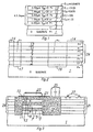
- FIGURE 1 there is shown a six layer reflector with a nearly short circuit or low impedance termination to the TFR. This can be fabricated for use in accordance with the present teachings. There is shown a p+ silicon substrate 1 over which has been deposited a first n- layer 3 over which are successive layers 5, 7, 9, 11 and 13 which are alternate layers of p+ and n- silicon, the p+ layer being converted later to porous silicon and the n- layer being preserved as non-porous silicon.
- the porous silicon layers have a ⁇ /4 thickness of 0.722 ⁇ m and a characteristic impedance of 5 x 10 6 kg/m 2 s and the n- layers have a ⁇ /4 thickness of 1.194 ⁇ m and a characteristic impedance of 20 x10 6 kg/m 2 s.
- FIGURE 2 there is shown a schematic diagram of the P+ diffusion and masking required prior to anodization to convert the P+ layers into porous silicon whereas the N- layers are not so converted to provide a structure of the type shown in FIGURE 3.
- the P+ silicon substrate 1 over which have been formed alternating N- layers 3, 7, 11 interleaved with P+ layers 5, 9, 13.
- the structure is then masked, leaving only the surrounding regions 17,19 exposed and sufficient P-type dopant is implanted/diffused and to a sufficient depth such that all unmasked portions of N-layers 3, 7, 11 are converted to P+ and the dopant extends partly into the substrate 1.
- the mask is then removed and the structure is again masked with an appropriate mask 14 which exposes the surrounding regions 17,19 and the layered structure surrounding by the surrounding regions.
- anodization now takes place, only the exposed parts of the P+ layers and the surrounding regions 17,19 are made porous with the N- regions and the regions under the mask 14, numbered 29 in FIGURE 3, remain intact.
- FIGURE 3 there is shown an integrated circuit having a TFR with an integrated acoustic reflector design.
- the circuit includes the substrate 1 of FIGURE 1 and the reflector as shown by the alternate layers 3, 5, 7, 9, 11 and 13 which are the same as in FIGURE 1 to form the reflector 15.
- the reflector 15 is surrounded by p+ diffusion to substrate connection regions which are converted to porous silicon 17, 19 together with layers 5, 9 and 13.
- the substrate connection region 17, 19 can have varying widths around the acoustic reflector, or defined as a separate region to facilitate RLC passive integration 25.
- a region of interconnect 21 is disposed over the reflector 15 and extends over the surrounding region 19, this interconnect, for example, coupling a piezoelectric resonator 23, disposed over the reflector and formed from, for example, zinc oxide or aluminum nitride to passive circuit elements 25 disposed over the surrounding region 19. Also shown are active elements 27 which are formed in standard manner in the n- region 29 which is formed over the substrate 1 and external to the surrounding region 17, 19. Connection among the various elements shown is by standard interconnect.
Landscapes
- Physics & Mathematics (AREA)
- Acoustics & Sound (AREA)
- Piezo-Electric Or Mechanical Vibrators, Or Delay Or Filter Circuits (AREA)
- Surface Acoustic Wave Elements And Circuit Networks Thereof (AREA)
- Semiconductor Integrated Circuits (AREA)
- Piezo-Electric Transducers For Audible Bands (AREA)
Claims (21)
- Integrierte Resonatorschaltung mit:einem Stapel mit mehreren alternierend nicht porösen Siliciumschichten und porösen Siliciumschichten (3, 5, 7, 9, 11, 13), wobei die Schichten von einem alternierend entgegengesetzten Leitfähigkeitstyp sind, und einer Schicht eines ersten Leitfähigkeitstyps, die über einem Abschnitt eines Siliciumsubstrats (1) aufgebracht ist, undeinem TFR-Resonator (23), der über dem Stapel angeordnet ist.
- Schaltung nach Anspruch 1, welche weiter aufweist:einen Rauschisolator (17, 19), der entlang Seitenwänden des Stapels angeordnet ist und sich in das Substrat erstreckt.
- Schaltung nach Anspruch 2, wobei der Rauschisolator den Stapel vollständig umgibt.
- Schaltung nach Anspruch 2 oder 3, wobei der Rauschisolator aus porösem Silicium besteht.
- Schaltung nach einem der vorstehenden Ansprüche, wobei die Schichten des Stapels eine Dicke von einem Viertel der Wellenlänge bei einer Frequenz des Resonators aufweisen.
- Integrierte Resonatorschaltung nach einem der Ansprüche 2 bis 5, welche weiter aufweist:einen Bereich aus Silicium (29), der auf dem Substrat angeordnet ist und von dem Stapel durch den Rauschisolator getrennt ist, undwenigstens eine von einer aktiven und/oder einer passiven Vorrichtung (25, 27), die auf dem Siliciumbereich oder in diesem angeordnet ist.
- Schaltung nach Anspruch 6, welche weiter aufweist:wenigstens eine passive Vorrichtung (25), die über dem Rauschisolator angeordnet ist.
- Schaltung nach Anspruch 6 oder 7, welche weiter aufweist:eine Zwischenverbindung (21), die den Resonator und die wenigstens eine aktive und/oder passive Vorrichtung verbindet.
- Schaltung nach einem der Ansprüche 6 bis 8, wobei der Rauschisolator (17, 19) den Stapel vollständig umgibt.
- Schaltung nach einem der Ansprüche 6 bis 9, wobei der Rauschisolator (17, 19) aus porösem Silicium besteht.
- Schaltung nach einem der Ansprüche 6 bis 10, wobei die Schichten des Stapels eine Dicke von einem Viertel der Wellenlänge bei einer Frequenz des Resonators aufweisen.
- Verfahren zum Bilden einer integrierten Resonatorschaltung, bei dem:ein Stapel gebildet wird, der mehrere alternierend nicht poröse Siliciumschichten und poröse Siliciumschichten (3, 5, 7, 9, 11, 13) aufweist, wobei die Schichten alternierend entgegengesetzten Leitfähigkeitstypen angehören und eine Schicht eines ersten Leitfähigkeitstyps über einem Teil eines Substrats (1) angeordnet ist, undein TFR-Resonator (23) gebildet wird, der über dem Stapel angeordnet wird.
- Verfahren nach Anspruch 12, bei dem weiter:ein Rauschisolator (17, 19) entlang den Seitenwänden des Stapels bereitgestellt wird und sich in das Substrat erstreckt.
- Verfahren nach Anspruch 13, wobei bei dem Schritt des Bereitstellens des Rauschisolators ein Rauschisolator bereitgestellt wird, der den Stapel vollständig umgibt und aus porösem Silicium besteht.
- Verfahren nach einem der Ansprüche 12 bis 14, wobei bei dem Schritt des Bildens des Stapels ein Stapel aus Schichten gebildet wird, die eine Dicke aufweisen, die ein Viertel der Wellenlänge bei der Frequenz des Resonators beträgt.
- Verfahren zum Bilden einer integrierten Resonatorschaltung nach Anspruch 13, 14 oder 15, soweit letzterer von Anspruch 13 abhängt, bei dem weiter:ein Siliciumbereich (29) gebildet wird, der auf dem Substrat angeordnet ist und durch den Rauschisolator von dem Stapel getrennt ist, undwenigstens eine aktive und/oder eine passive Vorrichtung (25, 27) gebildet wird, die auf oder in dem Siliciumbereich angeordnet ist.
- Verfahren nach Anspruch 16, bei dem weiter:wenigstens eine passive Vorrichtung (25) gebildet wird, die über dem Rauschisolator angeordnet ist.
- Verfahren nach Anspruch 17, bei dem weiter:eine Zwischenverbindung (21) gebildet wird, die den Resonator und wenigstens eine von der aktiven und/oder der passiven Vorrichtung verbindet.
- Verfahren nach einem der Ansprüche 16 bis 18, wobei beim Schritt des Bildens des Rauschisolators ein Rauschisolator gebildet wird, der den Stapel vollständig umgibt.
- Verfahren nach einem der Ansprüche 16 bis 19, wobei beim Schritt des Bildens des Rauschisolators ein Rauschisolator gebildet wird, der poröses Silicium aufweist.
- Verfahren nach einem der Ansprüche 16 bis 20, wobei beim Schritt des Bildens des Stapels ein Stapel gebildet wird, wobei Schichten des Stapels eine Dicke von einem Viertel der Wellenlänge bei der Frequenz des Resonators aufweisen.
Applications Claiming Priority (2)
| Application Number | Priority Date | Filing Date | Title |
|---|---|---|---|
| US9986498P | 1998-09-11 | 1998-09-11 | |
| US99864P | 1998-09-11 |
Publications (3)
| Publication Number | Publication Date |
|---|---|
| EP0986172A2 EP0986172A2 (de) | 2000-03-15 |
| EP0986172A3 EP0986172A3 (de) | 2000-10-18 |
| EP0986172B1 true EP0986172B1 (de) | 2004-12-01 |
Family
ID=22276990
Family Applications (1)
| Application Number | Title | Priority Date | Filing Date |
|---|---|---|---|
| EP99202912A Expired - Lifetime EP0986172B1 (de) | 1998-09-11 | 1999-09-09 | Integrierter akustischer Dünnfilmresonator |
Country Status (5)
| Country | Link |
|---|---|
| US (1) | US6297515B1 (de) |
| EP (1) | EP0986172B1 (de) |
| JP (1) | JP2000101386A (de) |
| AT (1) | ATE284091T1 (de) |
| DE (1) | DE69922311T2 (de) |
Families Citing this family (13)
| Publication number | Priority date | Publication date | Assignee | Title |
|---|---|---|---|---|
| DE19931297A1 (de) * | 1999-07-07 | 2001-01-11 | Philips Corp Intellectual Pty | Volumenwellen-Filter |
| GB0014963D0 (en) * | 2000-06-20 | 2000-08-09 | Koninkl Philips Electronics Nv | A bulk acoustic wave device |
| US6496085B2 (en) * | 2001-01-02 | 2002-12-17 | Nokia Mobile Phones Ltd | Solidly mounted multi-resonator bulk acoustic wave filter with a patterned acoustic mirror |
| FR2823032B1 (fr) * | 2001-04-03 | 2003-07-11 | St Microelectronics Sa | Resonateur electromecanique a poutre vibrante |
| DE10225202B4 (de) * | 2002-06-06 | 2017-06-01 | Epcos Ag | Mit akustischen Wellen arbeitendes Bauelement mit einem Anpassnetzwerk |
| FR2890490A1 (fr) * | 2005-09-05 | 2007-03-09 | St Microelectronics Sa | Support de resonateur acoustique et circuit integre correspondant |
| JP2007129391A (ja) * | 2005-11-02 | 2007-05-24 | Matsushita Electric Ind Co Ltd | 音響共振器及びフィルタ |
| JP4804961B2 (ja) * | 2006-03-03 | 2011-11-02 | オリンパスメディカルシステムズ株式会社 | 超音波振動子及びそれを搭載した体腔内超音波診断装置 |
| WO2012137574A1 (ja) * | 2011-04-01 | 2012-10-11 | ルネサスエレクトロニクス株式会社 | 半導体装置およびその製造方法ならびに携帯電話機 |
| JP6368298B2 (ja) * | 2015-12-14 | 2018-08-01 | 太陽誘電株式会社 | 圧電薄膜共振器、フィルタおよびデュプレクサ |
| JP2022541172A (ja) * | 2019-07-19 | 2022-09-22 | アイキューイー ピーエルシー | 調整可能な誘電率及び調整可能な熱伝導率を有する半導体材料 |
| US20220140812A1 (en) * | 2020-10-30 | 2022-05-05 | RF360 Europe GmbH | Multi mirror stack |
| CN121585125A (zh) * | 2022-12-30 | 2026-02-27 | 泉州市三安集成电路有限公司 | 一种滤波器器件 |
Family Cites Families (6)
| Publication number | Priority date | Publication date | Assignee | Title |
|---|---|---|---|---|
| US5367308A (en) * | 1992-05-29 | 1994-11-22 | Iowa State University Research Foundation, Inc. | Thin film resonating device |
| US5864261A (en) * | 1994-05-23 | 1999-01-26 | Iowa State University Research Foundation | Multiple layer acoustical structures for thin-film resonator based circuits and systems |
| US5821833A (en) * | 1995-12-26 | 1998-10-13 | Tfr Technologies, Inc. | Stacked crystal filter device and method of making |
| US5936150A (en) * | 1998-04-13 | 1999-08-10 | Rockwell Science Center, Llc | Thin film resonant chemical sensor with resonant acoustic isolator |
| US6114635A (en) * | 1998-07-14 | 2000-09-05 | Tfr Technologies, Inc. | Chip-scale electronic component package |
| US6107721A (en) * | 1999-07-27 | 2000-08-22 | Tfr Technologies, Inc. | Piezoelectric resonators on a differentially offset reflector |
-
1999
- 1999-09-09 AT AT99202912T patent/ATE284091T1/de not_active IP Right Cessation
- 1999-09-09 DE DE69922311T patent/DE69922311T2/de not_active Expired - Lifetime
- 1999-09-09 EP EP99202912A patent/EP0986172B1/de not_active Expired - Lifetime
- 1999-09-10 JP JP11257524A patent/JP2000101386A/ja not_active Abandoned
- 1999-09-10 US US09/393,777 patent/US6297515B1/en not_active Expired - Lifetime
Also Published As
| Publication number | Publication date |
|---|---|
| EP0986172A3 (de) | 2000-10-18 |
| US6297515B1 (en) | 2001-10-02 |
| ATE284091T1 (de) | 2004-12-15 |
| DE69922311D1 (de) | 2005-01-05 |
| DE69922311T2 (de) | 2005-12-01 |
| EP0986172A2 (de) | 2000-03-15 |
| JP2000101386A (ja) | 2000-04-07 |
Similar Documents
| Publication | Publication Date | Title |
|---|---|---|
| US8098118B2 (en) | Bandpass filter and process of fabricating the same | |
| US6601276B2 (en) | Method for self alignment of patterned layers in thin film acoustic devices | |
| US9209776B2 (en) | Method of manufacturing an electrical resonator | |
| EP1253713B1 (de) | Regelung von effektiven Kopplungskoeffizienten in Dünnschichtresonatoren mit akustischen Vollumenwellen | |
| US5853601A (en) | Top-via etch technique for forming dielectric membranes | |
| US6297515B1 (en) | Integrated acoustic thin film resonator | |
| US12588414B2 (en) | Hybrid structure for a surface acoustic wave device | |
| KR100565799B1 (ko) | 일체화된 FBAR 및 Isolation부를 사용하여제조된 듀플렉서 및 그 제조 방법 | |
| US20070096851A1 (en) | Bulk acoustic resonator and filter element | |
| CN101340181A (zh) | 薄膜体声波谐振器以及制造该谐振器滤波器,复合电子元器件和通信器件的方法 | |
| CN117459021B (zh) | 一种集成无源器件的体声波单片混合滤波器及其制备方法 | |
| CN111917393A (zh) | 体声波谐振器及制造方法、体声波谐振器组件、滤波器及电子设备 | |
| CN114257204B (zh) | 具有声阻层的体声波谐振器及其组件和制造方法、滤波器和电子设备 | |
| US20030117236A1 (en) | Multi-frequency thin film resonators | |
| EP1471636B1 (de) | Dünnschicht-Volumenwellen-Resonator (FBAR) mit Luftspalt und Herstellungsmethode dafür | |
| EP0932204A1 (de) | Intergrierter Schaltkreis und Verfahren für Hochfrequenzanwendungen | |
| EP1175727B1 (de) | Herstellungsverfahren einer hybriden integrierten schaltung mit einem halbleiterbauelement und einem piezoelektrischen filter | |
| US11611328B2 (en) | Fin bulk acoustic resonator technology for UHF and SHF signal processing | |
| WO2006034119A1 (en) | BST INTEGRATION USING THIN BUFFER LAYER GROWN DIRECTLY ONTO SiO2/Si SUBSTRATE | |
| US20220140812A1 (en) | Multi mirror stack | |
| TW202404257A (zh) | 體聲波裝置及體聲波裝置的製造方法 | |
| KR20200025471A (ko) | 적층 pcb 제조 공법을 이용한 fbar 듀플렉서 설계 방법 및 그 방법으로 제작된 fbar 듀플렉서 | |
| KR20030025600A (ko) | 박막 벌크 어쿠스틱 공진기를 이용한 듀플렉서 제조방법 |
Legal Events
| Date | Code | Title | Description |
|---|---|---|---|
| PUAI | Public reference made under article 153(3) epc to a published international application that has entered the european phase |
Free format text: ORIGINAL CODE: 0009012 |
|
| AK | Designated contracting states |
Kind code of ref document: A2 Designated state(s): AT BE CH CY DE DK ES FI FR GB GR IE IT LI LU MC NL PT SE |
|
| AX | Request for extension of the european patent |
Free format text: AL;LT;LV;MK;RO;SI |
|
| PUAL | Search report despatched |
Free format text: ORIGINAL CODE: 0009013 |
|
| AK | Designated contracting states |
Kind code of ref document: A3 Designated state(s): AT BE CH CY DE DK ES FI FR GB GR IE IT LI LU MC NL PT SE |
|
| AX | Request for extension of the european patent |
Free format text: AL;LT;LV;MK;RO;SI |
|
| RIC1 | Information provided on ipc code assigned before grant |
Free format text: 7H 03H 9/00 A, 7H 03B 5/36 B, 7H 03H 9/17 B |
|
| 17P | Request for examination filed |
Effective date: 20010418 |
|
| AKX | Designation fees paid |
Free format text: AT BE CH CY DE DK ES FI FR GB GR IE IT LI LU MC NL PT SE |
|
| GRAP | Despatch of communication of intention to grant a patent |
Free format text: ORIGINAL CODE: EPIDOSNIGR1 |
|
| GRAS | Grant fee paid |
Free format text: ORIGINAL CODE: EPIDOSNIGR3 |
|
| GRAA | (expected) grant |
Free format text: ORIGINAL CODE: 0009210 |
|
| AK | Designated contracting states |
Kind code of ref document: B1 Designated state(s): AT BE CH CY DE DK ES FI FR GB GR IE IT LI LU MC NL PT SE |
|
| PG25 | Lapsed in a contracting state [announced via postgrant information from national office to epo] |
Ref country code: NL Free format text: LAPSE BECAUSE OF FAILURE TO SUBMIT A TRANSLATION OF THE DESCRIPTION OR TO PAY THE FEE WITHIN THE PRESCRIBED TIME-LIMIT Effective date: 20041201 Ref country code: LI Free format text: LAPSE BECAUSE OF FAILURE TO SUBMIT A TRANSLATION OF THE DESCRIPTION OR TO PAY THE FEE WITHIN THE PRESCRIBED TIME-LIMIT Effective date: 20041201 Ref country code: IT Free format text: LAPSE BECAUSE OF FAILURE TO SUBMIT A TRANSLATION OF THE DESCRIPTION OR TO PAY THE FEE WITHIN THE PRESCRIBED TIME-LIMIT;WARNING: LAPSES OF ITALIAN PATENTS WITH EFFECTIVE DATE BEFORE 2007 MAY HAVE OCCURRED AT ANY TIME BEFORE 2007. THE CORRECT EFFECTIVE DATE MAY BE DIFFERENT FROM THE ONE RECORDED. Effective date: 20041201 Ref country code: FI Free format text: LAPSE BECAUSE OF FAILURE TO SUBMIT A TRANSLATION OF THE DESCRIPTION OR TO PAY THE FEE WITHIN THE PRESCRIBED TIME-LIMIT Effective date: 20041201 Ref country code: CH Free format text: LAPSE BECAUSE OF FAILURE TO SUBMIT A TRANSLATION OF THE DESCRIPTION OR TO PAY THE FEE WITHIN THE PRESCRIBED TIME-LIMIT Effective date: 20041201 Ref country code: BE Free format text: LAPSE BECAUSE OF FAILURE TO SUBMIT A TRANSLATION OF THE DESCRIPTION OR TO PAY THE FEE WITHIN THE PRESCRIBED TIME-LIMIT Effective date: 20041201 Ref country code: AT Free format text: LAPSE BECAUSE OF FAILURE TO SUBMIT A TRANSLATION OF THE DESCRIPTION OR TO PAY THE FEE WITHIN THE PRESCRIBED TIME-LIMIT Effective date: 20041201 |
|
| REG | Reference to a national code |
Ref country code: GB Ref legal event code: FG4D |
|
| REG | Reference to a national code |
Ref country code: CH Ref legal event code: EP |
|
| REG | Reference to a national code |
Ref country code: IE Ref legal event code: FG4D |
|
| REF | Corresponds to: |
Ref document number: 69922311 Country of ref document: DE Date of ref document: 20050105 Kind code of ref document: P |
|
| PG25 | Lapsed in a contracting state [announced via postgrant information from national office to epo] |
Ref country code: SE Free format text: LAPSE BECAUSE OF FAILURE TO SUBMIT A TRANSLATION OF THE DESCRIPTION OR TO PAY THE FEE WITHIN THE PRESCRIBED TIME-LIMIT Effective date: 20050301 Ref country code: GR Free format text: LAPSE BECAUSE OF FAILURE TO SUBMIT A TRANSLATION OF THE DESCRIPTION OR TO PAY THE FEE WITHIN THE PRESCRIBED TIME-LIMIT Effective date: 20050301 Ref country code: DK Free format text: LAPSE BECAUSE OF FAILURE TO SUBMIT A TRANSLATION OF THE DESCRIPTION OR TO PAY THE FEE WITHIN THE PRESCRIBED TIME-LIMIT Effective date: 20050301 |
|
| PG25 | Lapsed in a contracting state [announced via postgrant information from national office to epo] |
Ref country code: ES Free format text: LAPSE BECAUSE OF FAILURE TO SUBMIT A TRANSLATION OF THE DESCRIPTION OR TO PAY THE FEE WITHIN THE PRESCRIBED TIME-LIMIT Effective date: 20050312 |
|
| NLV1 | Nl: lapsed or annulled due to failure to fulfill the requirements of art. 29p and 29m of the patents act | ||
| REG | Reference to a national code |
Ref country code: CH Ref legal event code: PL |
|
| ET | Fr: translation filed | ||
| PG25 | Lapsed in a contracting state [announced via postgrant information from national office to epo] |
Ref country code: IE Free format text: LAPSE BECAUSE OF NON-PAYMENT OF DUE FEES Effective date: 20050909 Ref country code: CY Free format text: LAPSE BECAUSE OF FAILURE TO SUBMIT A TRANSLATION OF THE DESCRIPTION OR TO PAY THE FEE WITHIN THE PRESCRIBED TIME-LIMIT Effective date: 20050909 |
|
| PG25 | Lapsed in a contracting state [announced via postgrant information from national office to epo] |
Ref country code: MC Free format text: LAPSE BECAUSE OF NON-PAYMENT OF DUE FEES Effective date: 20050930 Ref country code: LU Free format text: LAPSE BECAUSE OF NON-PAYMENT OF DUE FEES Effective date: 20050930 |
|
| PLBE | No opposition filed within time limit |
Free format text: ORIGINAL CODE: 0009261 |
|
| STAA | Information on the status of an ep patent application or granted ep patent |
Free format text: STATUS: NO OPPOSITION FILED WITHIN TIME LIMIT |
|
| 26N | No opposition filed |
Effective date: 20050902 |
|
| REG | Reference to a national code |
Ref country code: IE Ref legal event code: MM4A |
|
| PG25 | Lapsed in a contracting state [announced via postgrant information from national office to epo] |
Ref country code: PT Free format text: LAPSE BECAUSE OF NON-PAYMENT OF DUE FEES Effective date: 20050501 |
|
| PGFP | Annual fee paid to national office [announced via postgrant information from national office to epo] |
Ref country code: GB Payment date: 20140826 Year of fee payment: 16 Ref country code: FR Payment date: 20140825 Year of fee payment: 16 |
|
| PGFP | Annual fee paid to national office [announced via postgrant information from national office to epo] |
Ref country code: DE Payment date: 20140930 Year of fee payment: 16 |
|
| REG | Reference to a national code |
Ref country code: DE Ref legal event code: R119 Ref document number: 69922311 Country of ref document: DE |
|
| GBPC | Gb: european patent ceased through non-payment of renewal fee |
Effective date: 20150909 |
|
| REG | Reference to a national code |
Ref country code: FR Ref legal event code: ST Effective date: 20160531 |
|
| PG25 | Lapsed in a contracting state [announced via postgrant information from national office to epo] |
Ref country code: DE Free format text: LAPSE BECAUSE OF NON-PAYMENT OF DUE FEES Effective date: 20160401 Ref country code: GB Free format text: LAPSE BECAUSE OF NON-PAYMENT OF DUE FEES Effective date: 20150909 |
|
| PG25 | Lapsed in a contracting state [announced via postgrant information from national office to epo] |
Ref country code: FR Free format text: LAPSE BECAUSE OF NON-PAYMENT OF DUE FEES Effective date: 20150930 |