EP0986099A2 - Translator für versenkte Flip-Chip-Verpackung - Google Patents
Translator für versenkte Flip-Chip-Verpackung Download PDFInfo
- Publication number
- EP0986099A2 EP0986099A2 EP99306922A EP99306922A EP0986099A2 EP 0986099 A2 EP0986099 A2 EP 0986099A2 EP 99306922 A EP99306922 A EP 99306922A EP 99306922 A EP99306922 A EP 99306922A EP 0986099 A2 EP0986099 A2 EP 0986099A2
- Authority
- EP
- European Patent Office
- Prior art keywords
- bonding pads
- translator
- group
- interconnections
- pwb
- Prior art date
- Legal status (The legal status is an assumption and is not a legal conclusion. Google has not performed a legal analysis and makes no representation as to the accuracy of the status listed.)
- Ceased
Links
- 239000000758 substrate Substances 0.000 claims description 32
- 229910052710 silicon Inorganic materials 0.000 claims description 11
- 239000010703 silicon Substances 0.000 claims description 11
- 229910000679 solder Inorganic materials 0.000 claims description 7
- 229910052751 metal Inorganic materials 0.000 claims description 6
- 239000002184 metal Substances 0.000 claims description 6
- XUIMIQQOPSSXEZ-UHFFFAOYSA-N Silicon Chemical group [Si] XUIMIQQOPSSXEZ-UHFFFAOYSA-N 0.000 description 8
- 239000004020 conductor Substances 0.000 description 8
- 238000013461 design Methods 0.000 description 7
- 230000008901 benefit Effects 0.000 description 5
- 238000005516 engineering process Methods 0.000 description 5
- 239000000463 material Substances 0.000 description 5
- 238000000034 method Methods 0.000 description 3
- VYPSYNLAJGMNEJ-UHFFFAOYSA-N Silicium dioxide Chemical compound O=[Si]=O VYPSYNLAJGMNEJ-UHFFFAOYSA-N 0.000 description 2
- 229910052782 aluminium Inorganic materials 0.000 description 2
- XAGFODPZIPBFFR-UHFFFAOYSA-N aluminium Chemical compound [Al] XAGFODPZIPBFFR-UHFFFAOYSA-N 0.000 description 2
- 238000013459 approach Methods 0.000 description 2
- 239000000919 ceramic Substances 0.000 description 2
- 239000011248 coating agent Substances 0.000 description 2
- 238000000576 coating method Methods 0.000 description 2
- 238000007596 consolidation process Methods 0.000 description 2
- 229910052737 gold Inorganic materials 0.000 description 2
- 239000011810 insulating material Substances 0.000 description 2
- 239000004065 semiconductor Substances 0.000 description 2
- 238000004544 sputter deposition Methods 0.000 description 2
- 229910017813 Cu—Cr Inorganic materials 0.000 description 1
- 239000004593 Epoxy Substances 0.000 description 1
- 239000004642 Polyimide Substances 0.000 description 1
- 229910018885 Pt—Au Inorganic materials 0.000 description 1
- 229910045601 alloy Inorganic materials 0.000 description 1
- 239000000956 alloy Substances 0.000 description 1
- 238000003491 array Methods 0.000 description 1
- 230000008859 change Effects 0.000 description 1
- 229910052681 coesite Inorganic materials 0.000 description 1
- 229910052906 cristobalite Inorganic materials 0.000 description 1
- 239000003989 dielectric material Substances 0.000 description 1
- 239000011521 glass Substances 0.000 description 1
- 238000001465 metallisation Methods 0.000 description 1
- 238000012986 modification Methods 0.000 description 1
- 230000004048 modification Effects 0.000 description 1
- 238000004806 packaging method and process Methods 0.000 description 1
- 229920001721 polyimide Polymers 0.000 description 1
- 239000002861 polymer material Substances 0.000 description 1
- 230000008569 process Effects 0.000 description 1
- 239000000377 silicon dioxide Substances 0.000 description 1
- 229910052682 stishovite Inorganic materials 0.000 description 1
- 229910052905 tridymite Inorganic materials 0.000 description 1
Images


Classifications
-
- H—ELECTRICITY
- H01—ELECTRIC ELEMENTS
- H01L—SEMICONDUCTOR DEVICES NOT COVERED BY CLASS H10
- H01L23/00—Details of semiconductor or other solid state devices
- H01L23/52—Arrangements for conducting electric current within the device in operation from one component to another, i.e. interconnections, e.g. wires, lead frames
-
- H—ELECTRICITY
- H01—ELECTRIC ELEMENTS
- H01L—SEMICONDUCTOR DEVICES NOT COVERED BY CLASS H10
- H01L23/00—Details of semiconductor or other solid state devices
- H01L23/48—Arrangements for conducting electric current to or from the solid state body in operation, e.g. leads, terminal arrangements ; Selection of materials therefor
- H01L23/488—Arrangements for conducting electric current to or from the solid state body in operation, e.g. leads, terminal arrangements ; Selection of materials therefor consisting of soldered or bonded constructions
- H01L23/498—Leads, i.e. metallisations or lead-frames on insulating substrates, e.g. chip carriers
- H01L23/49827—Via connections through the substrates, e.g. pins going through the substrate, coaxial cables
-
- H—ELECTRICITY
- H01—ELECTRIC ELEMENTS
- H01L—SEMICONDUCTOR DEVICES NOT COVERED BY CLASS H10
- H01L23/00—Details of semiconductor or other solid state devices
- H01L23/12—Mountings, e.g. non-detachable insulating substrates
- H01L23/13—Mountings, e.g. non-detachable insulating substrates characterised by the shape
-
- H—ELECTRICITY
- H01—ELECTRIC ELEMENTS
- H01L—SEMICONDUCTOR DEVICES NOT COVERED BY CLASS H10
- H01L23/00—Details of semiconductor or other solid state devices
- H01L23/12—Mountings, e.g. non-detachable insulating substrates
- H01L23/14—Mountings, e.g. non-detachable insulating substrates characterised by the material or its electrical properties
- H01L23/147—Semiconductor insulating substrates
-
- H—ELECTRICITY
- H01—ELECTRIC ELEMENTS
- H01L—SEMICONDUCTOR DEVICES NOT COVERED BY CLASS H10
- H01L23/00—Details of semiconductor or other solid state devices
- H01L23/28—Encapsulations, e.g. encapsulating layers, coatings, e.g. for protection
- H01L23/31—Encapsulations, e.g. encapsulating layers, coatings, e.g. for protection characterised by the arrangement or shape
- H01L23/3107—Encapsulations, e.g. encapsulating layers, coatings, e.g. for protection characterised by the arrangement or shape the device being completely enclosed
- H01L23/3121—Encapsulations, e.g. encapsulating layers, coatings, e.g. for protection characterised by the arrangement or shape the device being completely enclosed a substrate forming part of the encapsulation
- H01L23/3128—Encapsulations, e.g. encapsulating layers, coatings, e.g. for protection characterised by the arrangement or shape the device being completely enclosed a substrate forming part of the encapsulation the substrate having spherical bumps for external connection
-
- H—ELECTRICITY
- H01—ELECTRIC ELEMENTS
- H01L—SEMICONDUCTOR DEVICES NOT COVERED BY CLASS H10
- H01L2224/00—Indexing scheme for arrangements for connecting or disconnecting semiconductor or solid-state bodies and methods related thereto as covered by H01L24/00
- H01L2224/01—Means for bonding being attached to, or being formed on, the surface to be connected, e.g. chip-to-package, die-attach, "first-level" interconnects; Manufacturing methods related thereto
- H01L2224/10—Bump connectors; Manufacturing methods related thereto
- H01L2224/15—Structure, shape, material or disposition of the bump connectors after the connecting process
- H01L2224/16—Structure, shape, material or disposition of the bump connectors after the connecting process of an individual bump connector
-
- H—ELECTRICITY
- H01—ELECTRIC ELEMENTS
- H01L—SEMICONDUCTOR DEVICES NOT COVERED BY CLASS H10
- H01L2924/00—Indexing scheme for arrangements or methods for connecting or disconnecting semiconductor or solid-state bodies as covered by H01L24/00
- H01L2924/01—Chemical elements
- H01L2924/01046—Palladium [Pd]
-
- H—ELECTRICITY
- H01—ELECTRIC ELEMENTS
- H01L—SEMICONDUCTOR DEVICES NOT COVERED BY CLASS H10
- H01L2924/00—Indexing scheme for arrangements or methods for connecting or disconnecting semiconductor or solid-state bodies as covered by H01L24/00
- H01L2924/01—Chemical elements
- H01L2924/01078—Platinum [Pt]
-
- H—ELECTRICITY
- H01—ELECTRIC ELEMENTS
- H01L—SEMICONDUCTOR DEVICES NOT COVERED BY CLASS H10
- H01L2924/00—Indexing scheme for arrangements or methods for connecting or disconnecting semiconductor or solid-state bodies as covered by H01L24/00
- H01L2924/01—Chemical elements
- H01L2924/01079—Gold [Au]
-
- H—ELECTRICITY
- H01—ELECTRIC ELEMENTS
- H01L—SEMICONDUCTOR DEVICES NOT COVERED BY CLASS H10
- H01L2924/00—Indexing scheme for arrangements or methods for connecting or disconnecting semiconductor or solid-state bodies as covered by H01L24/00
- H01L2924/15—Details of package parts other than the semiconductor or other solid state devices to be connected
- H01L2924/151—Die mounting substrate
- H01L2924/1515—Shape
- H01L2924/15153—Shape the die mounting substrate comprising a recess for hosting the device
-
- H—ELECTRICITY
- H01—ELECTRIC ELEMENTS
- H01L—SEMICONDUCTOR DEVICES NOT COVERED BY CLASS H10
- H01L2924/00—Indexing scheme for arrangements or methods for connecting or disconnecting semiconductor or solid-state bodies as covered by H01L24/00
- H01L2924/15—Details of package parts other than the semiconductor or other solid state devices to be connected
- H01L2924/151—Die mounting substrate
- H01L2924/1517—Multilayer substrate
- H01L2924/15172—Fan-out arrangement of the internal vias
- H01L2924/15173—Fan-out arrangement of the internal vias in a single layer of the multilayer substrate
-
- H—ELECTRICITY
- H05—ELECTRIC TECHNIQUES NOT OTHERWISE PROVIDED FOR
- H05K—PRINTED CIRCUITS; CASINGS OR CONSTRUCTIONAL DETAILS OF ELECTRIC APPARATUS; MANUFACTURE OF ASSEMBLAGES OF ELECTRICAL COMPONENTS
- H05K2201/00—Indexing scheme relating to printed circuits covered by H05K1/00
- H05K2201/10—Details of components or other objects attached to or integrated in a printed circuit board
- H05K2201/10431—Details of mounted components
- H05K2201/10439—Position of a single component
- H05K2201/10477—Inverted
Definitions
- This invention relates to flip chip integrated circuit (IC) packages and more specifically to IC packages in which IC chips are recessed into cavities in an interconnection substrate. More specifically it relates to a recessed chip interconnection arrangement in which a single IC chip is interconnected to a translator to provide increased interconnect density.
- IC integrated circuit
- Recessed chip IC packages are gaining acceptance in IC device interconnection technology because of efficient utilization of interconnect substrate area, low overall package profile, and reduced interconnection length.
- a variety of recessed chip package options are described and claimed in US Patent No. 5,608,262, issued March 4, 1997 which, for purposes of this disclosure, is incorporated herein by reference.
- Recessed chip packages are characterized by three components, a primary IC chip or chips, defined for the purpose of this exposition as a first level component, an intermediate interconnection substrate (IIS) which (in a conventional package) may be either an IC chip or a passive interconnection substrate, defined here as a second level component, and a system interconnection substrate (SIS) which is typically a printed circuit board (PCB) and defined as a third level component.
- IIS intermediate interconnection substrate
- SIS system interconnection substrate
- PCB printed circuit board
- system interconnection substrate can itself function as an intermediate interconnection substrate and attach to a fourth board level, with the second level components recessed into cavities in the fourth level component.
- Recessed cavity structures have efficient interconnection arrangements, but there is an ever growing need for denser interconnections and higher interconnection performance.
- the translator is silicon, and the power and ground planes comprise separate interconnection levels on the translator.
- the multilevel interconnection feature of the translator allows both consolidation of the number of power and ground interconnections at this board level, and re-routing of power and ground I/Os, and signal I/Os, to the next board level.
- the translator of the invention accommodates a single high pin count IC chip, and is made substantially larger than the IC chip. The large translator area allows both routing and fan out on the silicon translator.
- FIG. 1 An IC chip with a large area array of interconnection sites is shown in Fig. 1.
- the IC chip is designated 1 1, and the area array interconnections sites are designated 12, and 13.
- the interconnection sites are shown as square but can be round. In a typical illustration the bonding pads are shown, and these can be square but more often are round.
- the three rows of edge arrayed sites 12, shown with an "x" are signal I/Os, and the interior sites 1 3,without an "x", are power and ground. These assignments can be changed depending on the circuit design, i.e. the pins can be mixed between signal and power/ground.
- Fig. 1 shows a total of 400 IC chip interconnection sites, with 196 assigned to power and ground, and 204 assigned to signal. In state of the art IC chips, the combined number of I/O interconnections may be much larger than 400, which more closely represents the interconnection challenge that is addressed by this invention.
- the improved interconnection approach is to use a translator for the second interconnect level, i.e. the substrate to which the IC chip is bonded, and to construct the translator as a large module with multilevel interconnections, so that the large array of interconnections can be accommodated and can cross over, re-route, and fan out.
- the added area for the translator depends on the number of area array interconnections and the pitch desired for these interconnections. In a typical arrangement according to the invention, the area of the translator is at least 4, and preferably 6, times the area of the IC chip.
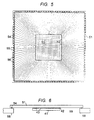
- a translator for interconnecting the IC chip of Fig. 1 according to the invention is shown in Fig. 2.
- the central portion of the translator 21 accommodates the IC chip, which flip-chip bonded to the translator.
- the position of the IC chip is shown at 15 in phantom.
- the array of IC interconnection sites on the translator mirrors the array on the IC chip.
- the translator 21 shown in Fig. 2 has an area approximately 7 times the area of the IC chip.
- the added area outside the IC chip area accommodates interconnection sites 22. This added area is referred to herein as the outboard area, and the interconnection sites in this area are for connections to the next board level.
- the outboard area accommodates 320 interconnection sites. This number is less than the 400 interconnection sites on the IC chip and is a deliberate choice for reasons that will become apparent. It should be evident that pin for pin sites could be accommodated in the outboard area of the translator of Fig. 2, and still have substantially greater pitch than the pitch of the IC chip interconnections.
- This design also utilizes the large area of the translator 21 outboard of the chip site to fan out the large array of interconnections, i.e. to increase the pitch of the outboard interconnections that go to the next level.
- the advantage of having a large pitch at this level in the package is that the translator can be flip-bonded to a printed wiring board or a ball grid array (BGA) using large solder bumps or balls. Large solder interconnections are more reliable and can be made with higher yield.
- the bump or ball pads at the interconnection sites 22 are solder wettable pads of e.g. Cu-Cr alloy or Ti-Pt-Au.
- the pitch of the interconnections in the outboard will be larger than the pitch of the IC interconnections. If the outboard area is more than four times the IC chip area, the pitch of the interconnection sites in the outboard area will normally be at least twice the pitch of the IC interconnections at the IC chip site. The pitch is the center-to-center spacing between interconnections sites.
- FIG. 3 is a detailed view of a portion of the center of the section 3-3 of Fig. 2. An important feature of this package design is evident in this figure, where the multilevels of interconnection can be seen.
- the U-shape of each of the interconnections 36-41 represents the conventional solder wettable metal.
- the area array in the center of the IC chip site is for power and ground interconnections.
- the translator according to the invention has special features for power and ground interconnections.
- a single interconnect level is reserved for power, and another level, preferably isolated from the first level by intervening levels, is reserved for the ground interconnections.
- Fig. 3 shows four levels of interconnection 31, 32, 33, and 34.
- interlevel dielectric layers are not individually shown in the figures but it will be evident to those skilled in the art that there is a first interlevel dielectric layer between conductive layers 33 and 34, a second interlevel dielectric layer between conductive layers 32 and 33, a third interlevel dielectric layer between conductive layers 31 and 32, and a top dielectric layer between conductive layer 31 and the pads 36-41.
- the bottom conductive level, 34 is a ground plane, and the top level 31 is a power plane.
- the two intermediate conductive levels 32 and 33 are assigned to signal I/Os. Conductive levels 31-33 are each shown with conductor patterns to illustrate the multilevel concept.
- the conductor pattern for the second and third levels may be absent in this view.
- providing conductor patterns in the center section offers the designer the option of intermixing signal I/Os and power and ground I/Os at any location on the IC chip, and therefore at any corresponding location in the center of the translator.
- the arrangement shown, with the intermediate levels assigned to signal I/Os and the top and bottom levels to power and ground respectively, has the advantage of isolating power and ground, but other assignations are obviously useful.
- the bottom interconnect level 34 which may be assigned either power or ground, or both, but is preferably the ground plane, is shown as a continuous sheet since no interconnections are made through this level.
- the ground plane can be the substrate, e.g. doped silicon, but for higher conductivity the substrate can be coated with a more conductive material e.g. Al, Ti-Pd-Au, or Au.
- the interconnect level 31 is a mesh of conductive material with openings as shown.
- the interconnection sites 36 and 37 are connected to the ground plane 34, and interconnection sites 38, 39 and 41 are connected to the power plane 31.
- the power and ground planes extend throughout the translator area, so that any one of the pads 22 can be connected to power and ground by providing a via to level 31 or 34 at the desired site in the outboard region of the translator.
- FIG. 4 is a view of a portion of Fig. 2 along section 4-4.
- edge array interconnection sites 42, 43 and 44 are connected to interconnect level 32 using vias as shown, and interconnection sites 45 and 46 are connected to level 32.
- the conductor patterns for levels 32 and 33 are conventional, i.e. a single runner connecting site 42 with a selected site 22 in the outboard region.
- the power and ground interconnections from the IC chip are aggregated together on the power and ground plane sheets. As described above the ground sheet is continuous and the power sheet is a mesh. Interconnections are made to these sheets at any desired site 22 in the outboard region using an appropriate via. This allows the circuit designer the freedom to re-route power and ground, and to change the number of power and ground interconnections coming off the translator from the number coming on.
- Fig. 2 shows 204 IC chip signal I/O interconnection sites, and 196 power and ground interconnection sites. However, there are just 320 interconnection sites 22 in the outboard region of the translator. Typically, each signal I/O from the IC chip is interconnected pin for pin at each board level, which consumes 204 of the 320 sites, leaving 116 for power and ground. As is evident from the above description, the power and ground interconnections between board levels are not discrete. In a typical circuit design, there is a need for a large number of power and ground interconnection sites, spaced around the outboard region, but typically this number is significantly fewer than the number of power and ground interconnections that come off the IC chip.
- the translator of the invention serves both to consolidate the power and ground connections, and redistribute them spatially.
- This consolidation function at a board level that in the prior art has been primarily a 1 for 1 pass through level, is an important advance in recessed flip chip packaging. Reducing power and ground interconnections by, e.g., at least 10% is regarded as significant.
- the ability to design crossovers at this board level, to achieve re-routing, to isolate power and ground, and to achieve fan out represents a major advance in interconnect technology.
- the translator 21 is then ball or bump soldered, by a series of interconnections 51, to the next board level 52, with the IC chip recessed as shown.
- the interconnection level 52 is preferably a ball grid array which provides reliable bonding of the many I/O leads from the translator to the next board level.
- the board level 52 may be an intermediate board level, or may be the system printed wiring board (PWB), i.e. the mother board. In either case an opening is provided in this level where the IC chip is recessed.
- PWB system printed wiring board
- the solder balls interconnecting the translator 21 to the board 52 are substantially larger than those interconnecting the IC chip to the translator.
- the IC chip interconnections are typically flip-chip micro-joints of e.g. 50 to 200 microns in diameter, while the BGA balls are typically 20 to 100 mils in diameter.
- the invention is applicable to PWB interconnection arrangements wherein the cavity for the IC chip extends completely through the thickness of the board, and the IC chip is mounted so as to recess significantly below the surface of the board, thus reducing the package profile.
- These structures, and the cavity for the IC chip are quadrangular in shape, and frequently square in shape.
- recessed chip packages can be made with the IC chip recessed into a depression, i.e. the cavity for the IC chip extends only partially through the printed wiring board to which the translator is attached.
- the term printed wiring board when used to define the invention refers to standard epoxy boards, for example, FR4, to ball grid array interconnect substrates, and any other suitable interconnect substrate.
- the material of the translator is preferably semiconductor, to match the coefficient of thermal expansion (CTE) of the IC chip. Most typically this will be silicon.
- CTE coefficient of thermal expansion
- An advantage of using silicon is that can be sufficiently conductive to serve as the bottom conductor level.
- Another advantage of using silicon is that the interconnection technology, for forming multiple levels of interconnections on the silicon, is well known and is used in principle in making the IC chip itself.
- the multilevel interconnections can be made using SiO 2 for the interlevel dielectric and aluminum for the metallization as is standard in Si IC technology.
- the interconnections on the translator are significantly larger than those on the IC chip and can be made with a less precise and less expensive technology.
- a preferred method for forming multilevel interconnections patterns on the translator i.e.
- spin on material for the interlevel dielectric.
- Spin-on materials include spin-on-glass (SOG) and a variety of known polymer materials such as polyimide.
- the multilayer conductor patterns may be made with any suitable metal, e.g. copper, aluminum, Au, Ti-Pd-Au, etc.
- the vias can be made by any suitable coating technique, e.g. sputtering. The thickness of the layers 31-34 and the interlevel dielectrics is small, so that coating the vias with a conventional sputtering process is not difficult. Via plugs can be used if desired.
- advantages of the invention e.g. the large area interconnection substrate with multilevel interconnect capability, can also be realized using other materials, notably ceramic. If an insulating material such as ceramic is used, a metal layer can be deposited on the insulating material for the bottom interconnection level.
- the invention primarily addresses IC packages wherein the IC has more than 400 I/Os.
- the size of the translator should be substantially larger than the IC to accommodate this large number of interconnections in the outboard region of the translator.
- the longest dimension (length) of the translator will exceed the longest dimension of the IC by at least a factor of 2, and preferably 2.5.
- the translator area will in most cases exceed the IC chip area by a factor of at least 4, and preferably by a factor of at least 6.
Applications Claiming Priority (2)
| Application Number | Priority Date | Filing Date | Title |
|---|---|---|---|
| US149804 | 1998-09-08 | ||
| US09/149,804 US6160715A (en) | 1998-09-08 | 1998-09-08 | Translator for recessed flip-chip package |
Publications (2)
| Publication Number | Publication Date |
|---|---|
| EP0986099A2 true EP0986099A2 (de) | 2000-03-15 |
| EP0986099A3 EP0986099A3 (de) | 2005-06-29 |
Family
ID=22531866
Family Applications (1)
| Application Number | Title | Priority Date | Filing Date |
|---|---|---|---|
| EP99306922A Ceased EP0986099A3 (de) | 1998-09-08 | 1999-08-31 | Translator für versenkte Flip-Chip-Verpackung |
Country Status (4)
| Country | Link |
|---|---|
| US (1) | US6160715A (de) |
| EP (1) | EP0986099A3 (de) |
| JP (1) | JP3803213B2 (de) |
| KR (1) | KR100754752B1 (de) |
Families Citing this family (13)
| Publication number | Priority date | Publication date | Assignee | Title |
|---|---|---|---|---|
| JP2000223657A (ja) * | 1999-02-03 | 2000-08-11 | Rohm Co Ltd | 半導体装置およびそれに用いる半導体チップ |
| US6972379B2 (en) * | 2000-05-26 | 2005-12-06 | Visteon Global Technologies, Inc. | Circuit board and a method for making the same |
| US6775906B1 (en) * | 2000-10-20 | 2004-08-17 | Silverbrook Research Pty Ltd | Method of manufacturing an integrated circuit carrier |
| US7902679B2 (en) | 2001-03-05 | 2011-03-08 | Megica Corporation | Structure and manufacturing method of a chip scale package with low fabrication cost, fine pitch and high reliability solder bump |
| US6818545B2 (en) * | 2001-03-05 | 2004-11-16 | Megic Corporation | Low fabrication cost, fine pitch and high reliability solder bump |
| US20030089998A1 (en) * | 2001-11-09 | 2003-05-15 | Chan Vincent K. | Direct interconnect multi-chip module, method for making the same and electronic package comprising same |
| US20030102159A1 (en) * | 2001-12-04 | 2003-06-05 | Loo Mike C. | Optimum power and ground bump pad and bump patterns for flip chip packaging |
| JP2003204209A (ja) * | 2002-01-07 | 2003-07-18 | Kyocera Corp | 高周波用配線基板 |
| US7276802B2 (en) * | 2002-04-15 | 2007-10-02 | Micron Technology, Inc. | Semiconductor integrated circuit package having electrically disconnected solder balls for mounting |
| US7087988B2 (en) | 2002-07-30 | 2006-08-08 | Kabushiki Kaisha Toshiba | Semiconductor packaging apparatus |
| US6744131B1 (en) * | 2003-04-22 | 2004-06-01 | Xilinx, Inc. | Flip chip integrated circuit packages accommodating exposed chip capacitors while providing structural rigidity |
| US7269813B2 (en) * | 2004-11-19 | 2007-09-11 | Alcatel | Off-width pitch for improved circuit card routing |
| CN104245203B (zh) * | 2012-03-05 | 2016-10-12 | 株式会社村田制作所 | 接合方法、电子装置的制造方法和电子部件 |
Citations (4)
| Publication number | Priority date | Publication date | Assignee | Title |
|---|---|---|---|---|
| US5084961A (en) * | 1990-04-09 | 1992-02-04 | Micro Gijutsu Kenkyujyo Co., Ltd. | Method of mounting circuit on substrate and circuit substrate for use in the method |
| EP0638931A2 (de) * | 1993-08-12 | 1995-02-15 | Fujitsu Limited | Mehrchipmodul |
| US5608262A (en) * | 1995-02-24 | 1997-03-04 | Lucent Technologies Inc. | Packaging multi-chip modules without wire-bond interconnection |
| US5728606A (en) * | 1995-01-25 | 1998-03-17 | International Business Machines Corporation | Electronic Package |
Family Cites Families (3)
| Publication number | Priority date | Publication date | Assignee | Title |
|---|---|---|---|---|
| US5490324A (en) * | 1993-09-15 | 1996-02-13 | Lsi Logic Corporation | Method of making integrated circuit package having multiple bonding tiers |
| US5906042A (en) * | 1995-10-04 | 1999-05-25 | Prolinx Labs Corporation | Method and structure to interconnect traces of two conductive layers in a printed circuit board |
| US5796170A (en) * | 1996-02-15 | 1998-08-18 | Northern Telecom Limited | Ball grid array (BGA) integrated circuit packages |
-
1998
- 1998-09-08 US US09/149,804 patent/US6160715A/en not_active Expired - Lifetime
-
1999
- 1999-08-31 EP EP99306922A patent/EP0986099A3/de not_active Ceased
- 1999-09-07 JP JP25301799A patent/JP3803213B2/ja not_active Expired - Lifetime
- 1999-09-08 KR KR1019990038064A patent/KR100754752B1/ko not_active IP Right Cessation
Patent Citations (4)
| Publication number | Priority date | Publication date | Assignee | Title |
|---|---|---|---|---|
| US5084961A (en) * | 1990-04-09 | 1992-02-04 | Micro Gijutsu Kenkyujyo Co., Ltd. | Method of mounting circuit on substrate and circuit substrate for use in the method |
| EP0638931A2 (de) * | 1993-08-12 | 1995-02-15 | Fujitsu Limited | Mehrchipmodul |
| US5728606A (en) * | 1995-01-25 | 1998-03-17 | International Business Machines Corporation | Electronic Package |
| US5608262A (en) * | 1995-02-24 | 1997-03-04 | Lucent Technologies Inc. | Packaging multi-chip modules without wire-bond interconnection |
Also Published As
| Publication number | Publication date |
|---|---|
| JP3803213B2 (ja) | 2006-08-02 |
| KR100754752B1 (ko) | 2007-09-05 |
| KR20000022977A (ko) | 2000-04-25 |
| EP0986099A3 (de) | 2005-06-29 |
| JP2000091462A (ja) | 2000-03-31 |
| US6160715A (en) | 2000-12-12 |
Similar Documents
| Publication | Publication Date | Title |
|---|---|---|
| US6175158B1 (en) | Interposer for recessed flip-chip package | |
| US6154370A (en) | Recessed flip-chip package | |
| EP0559366B1 (de) | Dreidimensionale gestapelte Mehrchip-Halbleiteranordnung und Verfahren zum Herstellen derselben | |
| US8492870B2 (en) | Semiconductor package with interconnect layers | |
| US6678167B1 (en) | High performance multi-chip IC package | |
| US7180170B2 (en) | Lead-free integrated circuit package structure | |
| US6894399B2 (en) | Microelectronic device having signal distribution functionality on an interfacial layer thereof | |
| US6461895B1 (en) | Process for making active interposer for high performance packaging applications | |
| US5935687A (en) | Three dimensional package and architecture for high performance computer | |
| US6081026A (en) | High density signal interposer with power and ground wrap | |
| US5776797A (en) | Three-dimensional flexible assembly of integrated circuits | |
| US6160715A (en) | Translator for recessed flip-chip package | |
| JPH0214598A (ja) | 電子素子取付用基板 | |
| CN1268245A (zh) | 封装集成电路的系统和方法 | |
| JP2005515611A (ja) | インターポーザを有する高性能低コスト超小型回路パッケージ | |
| TW201018026A (en) | Modification of connections between a die package and a system board | |
| US7078792B2 (en) | Universal interconnect die | |
| US6221693B1 (en) | High density flip chip BGA | |
| EP1361612B1 (de) | Organisches Flipchipbond-Substrat | |
| US6121678A (en) | Wrap-around interconnect for fine pitch ball grid array | |
| US5914533A (en) | Multilayer module with thinfilm redistribution area | |
| US6617243B1 (en) | Routing for multilayer ceramic substrates to reduce excessive via depth | |
| US20060231863A1 (en) | Manufacturing process of a chip package structure | |
| US5691569A (en) | Integrated circuit package that has a plurality of staggered pins | |
| CN217387150U (zh) | 半导体封装结构 |
Legal Events
| Date | Code | Title | Description |
|---|---|---|---|
| PUAI | Public reference made under article 153(3) epc to a published international application that has entered the european phase |
Free format text: ORIGINAL CODE: 0009012 |
|
| AK | Designated contracting states |
Kind code of ref document: A2 Designated state(s): AT BE CH CY DE DK ES FI FR GB GR IE IT LI LU MC NL PT SE |
|
| AX | Request for extension of the european patent |
Free format text: AL;LT;LV;MK;RO;SI |
|
| PUAL | Search report despatched |
Free format text: ORIGINAL CODE: 0009013 |
|
| AK | Designated contracting states |
Kind code of ref document: A3 Designated state(s): AT BE CH CY DE DK ES FI FR GB GR IE IT LI LU MC NL PT SE |
|
| AX | Request for extension of the european patent |
Extension state: AL LT LV MK RO SI |
|
| 17P | Request for examination filed |
Effective date: 20051222 |
|
| AKX | Designation fees paid |
Designated state(s): DE FR GB |
|
| STAA | Information on the status of an ep patent application or granted ep patent |
Free format text: STATUS: THE APPLICATION HAS BEEN REFUSED |
|
| 18R | Application refused |
Effective date: 20080210 |