EP0983617B1 - Vorrichtung zum übertragen von hochfrequenten signalen - Google Patents
Vorrichtung zum übertragen von hochfrequenten signalen Download PDFInfo
- Publication number
- EP0983617B1 EP0983617B1 EP98933463A EP98933463A EP0983617B1 EP 0983617 B1 EP0983617 B1 EP 0983617B1 EP 98933463 A EP98933463 A EP 98933463A EP 98933463 A EP98933463 A EP 98933463A EP 0983617 B1 EP0983617 B1 EP 0983617B1
- Authority
- EP
- European Patent Office
- Prior art keywords
- data lines
- glass
- lines
- signals
- copper
- Prior art date
- Legal status (The legal status is an assumption and is not a legal conclusion. Google has not performed a legal analysis and makes no representation as to the accuracy of the status listed.)
- Expired - Lifetime
Links
- 239000003365 glass fiber Substances 0.000 claims description 19
- 230000005540 biological transmission Effects 0.000 claims description 10
- 230000000295 complement effect Effects 0.000 claims description 8
- 239000004020 conductor Substances 0.000 claims description 3
- 239000000463 material Substances 0.000 abstract description 8
- 239000013307 optical fiber Substances 0.000 abstract description 4
- RYGMFSIKBFXOCR-UHFFFAOYSA-N Copper Chemical compound [Cu] RYGMFSIKBFXOCR-UHFFFAOYSA-N 0.000 description 21
- 229910052802 copper Inorganic materials 0.000 description 21
- 239000010949 copper Substances 0.000 description 21
- 239000011521 glass Substances 0.000 description 16
- 239000011347 resin Substances 0.000 description 6
- 229920005989 resin Polymers 0.000 description 6
- 230000008878 coupling Effects 0.000 description 5
- 238000010168 coupling process Methods 0.000 description 5
- 238000005859 coupling reaction Methods 0.000 description 5
- 238000000034 method Methods 0.000 description 5
- 238000012546 transfer Methods 0.000 description 5
- 238000004891 communication Methods 0.000 description 3
- 238000013461 design Methods 0.000 description 3
- 239000000835 fiber Substances 0.000 description 2
- 239000000758 substrate Substances 0.000 description 2
- 208000032365 Electromagnetic interference Diseases 0.000 description 1
- 239000000853 adhesive Substances 0.000 description 1
- 230000001070 adhesive effect Effects 0.000 description 1
- 238000010276 construction Methods 0.000 description 1
- 238000011161 development Methods 0.000 description 1
- 230000018109 developmental process Effects 0.000 description 1
- 239000003989 dielectric material Substances 0.000 description 1
- 239000011152 fibreglass Substances 0.000 description 1
- 230000036039 immunity Effects 0.000 description 1
- 238000004519 manufacturing process Methods 0.000 description 1
- 238000007747 plating Methods 0.000 description 1
- 238000012545 processing Methods 0.000 description 1
- 239000004753 textile Substances 0.000 description 1
Images

Classifications
-
- H—ELECTRICITY
- H01—ELECTRIC ELEMENTS
- H01P—WAVEGUIDES; RESONATORS, LINES, OR OTHER DEVICES OF THE WAVEGUIDE TYPE
- H01P3/00—Waveguides; Transmission lines of the waveguide type
- H01P3/02—Waveguides; Transmission lines of the waveguide type with two longitudinal conductors
- H01P3/08—Microstrips; Strip lines
-
- H—ELECTRICITY
- H05—ELECTRIC TECHNIQUES NOT OTHERWISE PROVIDED FOR
- H05K—PRINTED CIRCUITS; CASINGS OR CONSTRUCTIONAL DETAILS OF ELECTRIC APPARATUS; MANUFACTURE OF ASSEMBLAGES OF ELECTRICAL COMPONENTS
- H05K1/00—Printed circuits
- H05K1/02—Details
- H05K1/0213—Electrical arrangements not otherwise provided for
- H05K1/0237—High frequency adaptations
- H05K1/024—Dielectric details, e.g. changing the dielectric material around a transmission line
-
- H—ELECTRICITY
- H05—ELECTRIC TECHNIQUES NOT OTHERWISE PROVIDED FOR
- H05K—PRINTED CIRCUITS; CASINGS OR CONSTRUCTIONAL DETAILS OF ELECTRIC APPARATUS; MANUFACTURE OF ASSEMBLAGES OF ELECTRICAL COMPONENTS
- H05K1/00—Printed circuits
- H05K1/02—Details
- H05K1/03—Use of materials for the substrate
- H05K1/0313—Organic insulating material
- H05K1/0353—Organic insulating material consisting of two or more materials, e.g. two or more polymers, polymer + filler, + reinforcement
- H05K1/0366—Organic insulating material consisting of two or more materials, e.g. two or more polymers, polymer + filler, + reinforcement reinforced, e.g. by fibres, fabrics
-
- H—ELECTRICITY
- H05—ELECTRIC TECHNIQUES NOT OTHERWISE PROVIDED FOR
- H05K—PRINTED CIRCUITS; CASINGS OR CONSTRUCTIONAL DETAILS OF ELECTRIC APPARATUS; MANUFACTURE OF ASSEMBLAGES OF ELECTRICAL COMPONENTS
- H05K2201/00—Indexing scheme relating to printed circuits covered by H05K1/00
- H05K2201/02—Fillers; Particles; Fibers; Reinforcement materials
- H05K2201/0275—Fibers and reinforcement materials
- H05K2201/029—Woven fibrous reinforcement or textile
-
- H—ELECTRICITY
- H05—ELECTRIC TECHNIQUES NOT OTHERWISE PROVIDED FOR
- H05K—PRINTED CIRCUITS; CASINGS OR CONSTRUCTIONAL DETAILS OF ELECTRIC APPARATUS; MANUFACTURE OF ASSEMBLAGES OF ELECTRICAL COMPONENTS
- H05K2201/00—Indexing scheme relating to printed circuits covered by H05K1/00
- H05K2201/09—Shape and layout
- H05K2201/09209—Shape and layout details of conductors
- H05K2201/09218—Conductive traces
- H05K2201/09236—Parallel layout
Definitions
- the invention relates to a device according to the preamble of claim 1.
- the electrical signals are here in particular as control signals and / or message signals educated.
- message signals that follow an asynchronous transfer mode (ATM) can be transferred for example transfer rates of up to 830 Mbit / s
- ATM asynchronous transfer mode
- the modules previously used in the communication systems or printed circuit boards have connection structures in the prior art on where copper tracks are parallel to the edge of the respective PCB run (parallel to the edge). about these copper tracks then become the electrical ones in question Signals sent.
- the circuit boards used are made of a glass mat Made of material.
- the glass mats themselves exist from individual glass fiber bundles, soaked in resin and too a weave structure are formed. On the surface of one glass mat formed in this way then run copper tracks, via the electrical signals in practical operation become. A glass mat thus serves as a support for the copper tracks. To get a compact design, there are a number this glass mat with the associated copper lines glued together. This means that the majority of these copper tracks runs within the "layer block" thus formed. The latter then forms the actual circuit board. The connections are made on the surface by through-plating.
- the invention is therefore based on the object of a way to demonstrate how extremely high frequency message signals transmitted via copper lines in printed circuit boards of conventional type can be.
- a substrate material is known from the publication EP-A2-0309962 and a process for its manufacture discloses that the Solves the runtime difference problem by using the procedure manufactured substrate material consists of several layers and the fiber bundles of the individual layers under one predetermined angles are arranged to each other. Hereby This creates a quasi-isotropy.
- these are Publication no data lines carrying electrical signals and their arrangement in relation to the fiber bundle removable. This is not necessary because the quasi-isotropy has no time difference between the individual data lines can arise.
- the invention is characterized by the features of the Part of claim 1 solved.
- a particular advantage of the invention is that the data lines no longer parallel to the edges in the relevant glass mat material be led, but with a fixed predetermined defined angle to be rotated. This means ultimately that the data lines are no longer exclusive on a glass fiber or in the resin, but in the same way alternately over glass or resin run. This means that nothing arises during the transfer process Difference in the signal runtime.
- Conventional, inexpensive Printed circuit boards can also be used for transmission high-frequency signals are used, what with the multitude the circuit boards used a significant cost advantage is.
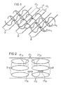
- FIG. 1 The structural design of a glass mat is shown in FIG. Accordingly, glass fiber bundles GF are shown first, which are arranged parallel to each other.
- the glass fiber bundle GF are made up of a plurality of fiberglass bundles as well existing chains K connected and held together. According to Figure 1, the chains K with "phase positions" of 180 ° woven around the glass fiber bundle GF. In this respect, this type of Structure quite similar to that of textiles.
- the chains K and glass fiber bundles arranged transversely to each other GF are not mechanically fixed on their own, however this device is still in a used as an adhesive material Resin soaked, making the glass mat a quasi homogeneous Maintains structure. In this way of building a glass mat is not a preferred direction in terms of orthogonality given. Both main axes have equal rights.
- the data lines LP carrying complementary signals are arranged parallel to the glass fiber bundles GF. These each have two pairs of copper lines LP a , LP b .
- the pairing of the data lines is not absolutely necessary. Rather, a complementary transmission of electrical signals can also take place via only one data line.
- FIG. 2 shows a side view of the glass fiber mat according to FIG. 1 just described, which in turn shows the glass fiber bundles GF which are guided in parallel and thus define the edges of the glass mat or the printed circuit board.
- data lines LP 1 LP 2 are now shown. It is essential that both data lines are to be regarded as alternatives and therefore not both are arranged in the glass mat in this form at the same time. This fact was taken into account in Figure 2 by the dashed line.
- the data line LP 1 consists of the copper line pairs LP 1a and LP 1b .
- the data line LP 2 is formed in the same way by a pair of copper lines LP 2a and LP 2b .
- this angle should be between 0.5 ° and 1 °. Other forms this angle is also conceivable. In any Case must be taken care of when choosing the angle that the data lines are not parallel to the glass fibers is arranged.
Landscapes
- Engineering & Computer Science (AREA)
- Microelectronics & Electronic Packaging (AREA)
- Structure Of Printed Boards (AREA)
- Optical Couplings Of Light Guides (AREA)
- Waveguides (AREA)
Abstract
Description
- Figur 1
- der konstruktive Aufbau einer Glasmatte,
- Figur 2
- die Seitenansicht einer Glasmatte,
- Figur 3
- der Signallauf beim Stand der Technik
Claims (3)
- Vorrichtung zum Übertragen von hochfrequenten Signalen, mit wenigstens einer aus einer Mehrzahl von Glasfaserbündeln gebildeten Glasfasermatte, die oberflächenseitig eine Mehrzahl von elektrische Signale führenden Datenleitungen aufweist und die gegebenenfalls mit weiteren derart gebildeten Glasfasermatten zu einer Leiterplatte zusammengefaßt wird,
dadurch gekennzeichnet, daß die elektrische Signale führenden Datenleitungen (LP1, LP2) unter einem vorgegebenen Winkel zu den Glasfaserbündeln (GF) angeordnet sind. - Vorrichtung nach Anspruch 1,
dadurch gekennzeichnet, daß die Datenleitungen (LP1, LP2) als Paar von Leiterbahnen (LP1a, LP1b; LP2a, LP2b) ausbildbar sind. - Vorrichtung nach Anspruch 2,
dadurch gekennzeichnet, daß über die Leiterbahnen eine komplementäre Übertragung der elektrischen Signale erfolgt.
Applications Claiming Priority (3)
| Application Number | Priority Date | Filing Date | Title |
|---|---|---|---|
| DE19721087 | 1997-05-20 | ||
| DE19721087A DE19721087C2 (de) | 1997-05-20 | 1997-05-20 | Vorrichtung zum Übertragen von hochfrequenten Signalen |
| PCT/DE1998/001262 WO1998053520A1 (de) | 1997-05-20 | 1998-05-06 | Vorrichtung zum übertragen von hochfrequenten signalen |
Publications (2)
| Publication Number | Publication Date |
|---|---|
| EP0983617A1 EP0983617A1 (de) | 2000-03-08 |
| EP0983617B1 true EP0983617B1 (de) | 2001-11-07 |
Family
ID=7829991
Family Applications (1)
| Application Number | Title | Priority Date | Filing Date |
|---|---|---|---|
| EP98933463A Expired - Lifetime EP0983617B1 (de) | 1997-05-20 | 1998-05-06 | Vorrichtung zum übertragen von hochfrequenten signalen |
Country Status (6)
| Country | Link |
|---|---|
| US (1) | US6304700B1 (de) |
| EP (1) | EP0983617B1 (de) |
| CA (1) | CA2290562C (de) |
| DE (2) | DE19721087C2 (de) |
| ES (1) | ES2167916T3 (de) |
| WO (1) | WO1998053520A1 (de) |
Families Citing this family (8)
| Publication number | Priority date | Publication date | Assignee | Title |
|---|---|---|---|---|
| US7043706B2 (en) * | 2003-03-11 | 2006-05-09 | Intel Corporation | Conductor trace design to reduce common mode cross-talk and timing skew |
| US7459200B2 (en) * | 2003-08-15 | 2008-12-02 | Intel Corporation | Circuit board design |
| US20050063637A1 (en) * | 2003-09-22 | 2005-03-24 | Mershon Jayne L. | Connecting a component with an embedded optical fiber |
| US20050063638A1 (en) * | 2003-09-24 | 2005-03-24 | Alger William O. | Optical fibers embedded in a printed circuit board |
| US7609125B2 (en) * | 2006-10-13 | 2009-10-27 | Avago Technologies Enterprise IP (Singapore) Pte. Ltd. | System, device and method for reducing cross-talk in differential signal conductor pairs |
| US8155497B2 (en) | 2007-10-18 | 2012-04-10 | The Regents Of The University Of Michigan | Fiber-based electric device |
| US7970242B2 (en) * | 2007-10-18 | 2011-06-28 | The Regents Of The University Of Michigan | Fiber-based electric device |
| CN101494948B (zh) * | 2008-01-24 | 2012-07-18 | 鸿富锦精密工业(深圳)有限公司 | 电路板及其设计方法 |
Family Cites Families (6)
| Publication number | Priority date | Publication date | Assignee | Title |
|---|---|---|---|---|
| US5183323A (en) * | 1982-09-29 | 1993-02-02 | Maurice Daniel | Flat panel illumination system |
| US5021928A (en) * | 1982-09-29 | 1991-06-04 | Maurice Daniel | Flat panel illumination system |
| EP0309982A3 (de) * | 1987-09-30 | 1990-09-12 | E.I. Du Pont De Nemours And Company | Polymerkeramische Verbundplatte |
| US4911543A (en) * | 1988-05-31 | 1990-03-27 | Hodgson R W | Microscope viewing apparatus for viewing a specimen image and an optical overlay pattern image in a comparison manner |
| US5418504A (en) | 1993-12-09 | 1995-05-23 | Nottenburg; Richard N. | Transmission line |
| US5736686A (en) * | 1995-03-01 | 1998-04-07 | Gtco Corporation | Illumination apparatus for a digitizer tablet with improved light panel |
-
1997
- 1997-05-20 DE DE19721087A patent/DE19721087C2/de not_active Expired - Lifetime
-
1998
- 1998-05-06 EP EP98933463A patent/EP0983617B1/de not_active Expired - Lifetime
- 1998-05-06 CA CA002290562A patent/CA2290562C/en not_active Expired - Lifetime
- 1998-05-06 DE DE59802072T patent/DE59802072D1/de not_active Expired - Lifetime
- 1998-05-06 US US09/424,412 patent/US6304700B1/en not_active Expired - Lifetime
- 1998-05-06 ES ES98933463T patent/ES2167916T3/es not_active Expired - Lifetime
- 1998-05-06 WO PCT/DE1998/001262 patent/WO1998053520A1/de not_active Ceased
Also Published As
| Publication number | Publication date |
|---|---|
| WO1998053520A1 (de) | 1998-11-26 |
| CA2290562A1 (en) | 1998-11-26 |
| DE19721087C2 (de) | 1999-10-14 |
| ES2167916T3 (es) | 2002-05-16 |
| US6304700B1 (en) | 2001-10-16 |
| DE19721087A1 (de) | 1998-11-26 |
| DE59802072D1 (de) | 2001-12-13 |
| CA2290562C (en) | 2008-04-01 |
| EP0983617A1 (de) | 2000-03-08 |
Similar Documents
| Publication | Publication Date | Title |
|---|---|---|
| DE10043761C2 (de) | HF-Verteilnetz | |
| EP0712267B1 (de) | Modulare Steuerungsanlage mit integriertem Feldbusanschluss | |
| DE69003891T2 (de) | Testvorrichtung für gedruckte Schaltungskarten und ihre Anwendung für das Testen von gedruckten Schaltungskarten, in Form einer Multiplex-Demultiplexeinrichtung für numerische Signale. | |
| EP0809222A1 (de) | Anordnung zur Datenübertragung in Prozessleitsystemen | |
| DE69735350T2 (de) | Lückenüberbrückungs-bussystem | |
| DE60115141T2 (de) | Doppelwendel-Flachbandleitungen | |
| DE60223398T2 (de) | Verfahren zum verbinden und prüfen von schnittstellen für faseroptische cwdm-systeme | |
| DE19721087C2 (de) | Vorrichtung zum Übertragen von hochfrequenten Signalen | |
| DE19629521C2 (de) | Matrixschaltplatine, Anordnung von Matrixschaltplatinen und Verbindungsstecker für Matrixschaltplatine | |
| EP3656132B1 (de) | Verwendung eines faseroptischen kreuzverbindungssystems | |
| DE102016100441A1 (de) | Empfangskoppler für eine kontaktlose Datenübertragungsstrecke | |
| EP0394725A2 (de) | Taktverteilereinrichtung | |
| DE60122639T2 (de) | Architektur eines passiven optischen Netzwerks | |
| EP2394499B1 (de) | Elektrooptisches steuer- oder regelgerät zum austausch von steuer- oder regelsignalen | |
| DE3641149A1 (de) | Breitband-raumvielfachkoppelfeld mit zwischenleitungsfuehrung in einer leiterplatte mit mehrlagigen leiterbahnen in mikrostrip-technik | |
| DE3715594C2 (de) | Anordnung zum Anschluß von Ausgangs- und Eingangsstufen einer Sende/Empfangseinrichtung | |
| CH676903A5 (en) | Information transmission system for train - uses coded microwave signals fed between successive train sections | |
| EP1065905A2 (de) | Lichtwellenleiter-Bussystem für Backplaneanwendungen | |
| EP0728581B1 (de) | Bussystem für eine Druckmaschine | |
| EP3542603B1 (de) | Elektrische steckbuchse | |
| DE102024201877A1 (de) | Board-to-Board-, BTB-Steckverbinder | |
| DE10157836B4 (de) | Signalverteilung zu einer Mehrzahl von Schaltungseinheiten | |
| EP2263333A1 (de) | Steuergerät mit einer einrichtung zur optischen datenübertragung | |
| DE2557179B1 (de) | Leitungsanordnung | |
| DE4017997A1 (de) | Optisches datenuebertragungssystem |
Legal Events
| Date | Code | Title | Description |
|---|---|---|---|
| PUAI | Public reference made under article 153(3) epc to a published international application that has entered the european phase |
Free format text: ORIGINAL CODE: 0009012 |
|
| 17P | Request for examination filed |
Effective date: 19991105 |
|
| AK | Designated contracting states |
Kind code of ref document: A1 Designated state(s): BE CH DE ES FR GB IT LI NL |
|
| GRAG | Despatch of communication of intention to grant |
Free format text: ORIGINAL CODE: EPIDOS AGRA |
|
| 17Q | First examination report despatched |
Effective date: 20010220 |
|
| GRAG | Despatch of communication of intention to grant |
Free format text: ORIGINAL CODE: EPIDOS AGRA |
|
| GRAH | Despatch of communication of intention to grant a patent |
Free format text: ORIGINAL CODE: EPIDOS IGRA |
|
| GRAH | Despatch of communication of intention to grant a patent |
Free format text: ORIGINAL CODE: EPIDOS IGRA |
|
| GRAA | (expected) grant |
Free format text: ORIGINAL CODE: 0009210 |
|
| AK | Designated contracting states |
Kind code of ref document: B1 Designated state(s): BE CH DE ES FR GB IT LI NL |
|
| REG | Reference to a national code |
Ref country code: CH Ref legal event code: EP |
|
| REF | Corresponds to: |
Ref document number: 59802072 Country of ref document: DE Date of ref document: 20011213 |
|
| REG | Reference to a national code |
Ref country code: CH Ref legal event code: NV Representative=s name: SIEMENS SCHWEIZ AG |
|
| REG | Reference to a national code |
Ref country code: GB Ref legal event code: IF02 |
|
| GBT | Gb: translation of ep patent filed (gb section 77(6)(a)/1977) |
Effective date: 20020124 |
|
| REG | Reference to a national code |
Ref country code: ES Ref legal event code: FG2A Ref document number: 2167916 Country of ref document: ES Kind code of ref document: T3 |
|
| PLBE | No opposition filed within time limit |
Free format text: ORIGINAL CODE: 0009261 |
|
| STAA | Information on the status of an ep patent application or granted ep patent |
Free format text: STATUS: NO OPPOSITION FILED WITHIN TIME LIMIT |
|
| 26N | No opposition filed | ||
| REG | Reference to a national code |
Ref country code: CH Ref legal event code: PCAR Free format text: SIEMENS SCHWEIZ AG;INTELLECTUAL PROPERTY FREILAGERSTRASSE 40;8047 ZUERICH (CH) |
|
| REG | Reference to a national code |
Ref country code: FR Ref legal event code: PLFP Year of fee payment: 19 |
|
| REG | Reference to a national code |
Ref country code: FR Ref legal event code: PLFP Year of fee payment: 20 |
|
| PGFP | Annual fee paid to national office [announced via postgrant information from national office to epo] |
Ref country code: NL Payment date: 20170509 Year of fee payment: 20 |
|
| PGFP | Annual fee paid to national office [announced via postgrant information from national office to epo] |
Ref country code: GB Payment date: 20170508 Year of fee payment: 20 Ref country code: FR Payment date: 20170526 Year of fee payment: 20 |
|
| PGFP | Annual fee paid to national office [announced via postgrant information from national office to epo] |
Ref country code: BE Payment date: 20170519 Year of fee payment: 20 Ref country code: IT Payment date: 20170526 Year of fee payment: 20 |
|
| REG | Reference to a national code |
Ref country code: CH Ref legal event code: PCOW Free format text: NEW ADDRESS: WERNER-VON-SIEMENS-STRASSE 1, 80333 MUENCHEN (DE) |
|
| PGFP | Annual fee paid to national office [announced via postgrant information from national office to epo] |
Ref country code: ES Payment date: 20170810 Year of fee payment: 20 Ref country code: CH Payment date: 20170807 Year of fee payment: 20 Ref country code: DE Payment date: 20170721 Year of fee payment: 20 |
|
| REG | Reference to a national code |
Ref country code: DE Ref legal event code: R071 Ref document number: 59802072 Country of ref document: DE |
|
| REG | Reference to a national code |
Ref country code: NL Ref legal event code: MK Effective date: 20180505 |
|
| REG | Reference to a national code |
Ref country code: CH Ref legal event code: PL |
|
| REG | Reference to a national code |
Ref country code: GB Ref legal event code: PE20 Expiry date: 20180505 |
|
| REG | Reference to a national code |
Ref country code: BE Ref legal event code: MK Effective date: 20180506 |
|
| PG25 | Lapsed in a contracting state [announced via postgrant information from national office to epo] |
Ref country code: GB Free format text: LAPSE BECAUSE OF EXPIRATION OF PROTECTION Effective date: 20180505 |
|
| REG | Reference to a national code |
Ref country code: ES Ref legal event code: FD2A Effective date: 20220128 |
|
| PG25 | Lapsed in a contracting state [announced via postgrant information from national office to epo] |
Ref country code: ES Free format text: LAPSE BECAUSE OF EXPIRATION OF PROTECTION Effective date: 20180507 |