EP0983607B1 - Bump forming method and bump bonder - Google Patents
Bump forming method and bump bonder Download PDFInfo
- Publication number
- EP0983607B1 EP0983607B1 EP98921766A EP98921766A EP0983607B1 EP 0983607 B1 EP0983607 B1 EP 0983607B1 EP 98921766 A EP98921766 A EP 98921766A EP 98921766 A EP98921766 A EP 98921766A EP 0983607 B1 EP0983607 B1 EP 0983607B1
- Authority
- EP
- European Patent Office
- Prior art keywords
- wire
- capillary
- clamper
- bump
- bonding
- Prior art date
- Legal status (The legal status is an assumption and is not a legal conclusion. Google has not performed a legal analysis and makes no representation as to the accuracy of the status listed.)
- Expired - Lifetime
Links
Images




Classifications
-
- H—ELECTRICITY
- H10—SEMICONDUCTOR DEVICES; ELECTRIC SOLID-STATE DEVICES NOT OTHERWISE PROVIDED FOR
- H10W—GENERIC PACKAGES, INTERCONNECTIONS, CONNECTORS OR OTHER CONSTRUCTIONAL DETAILS OF DEVICES COVERED BY CLASS H10
- H10W72/00—Interconnections or connectors in packages
- H10W72/071—Connecting or disconnecting
-
- B—PERFORMING OPERATIONS; TRANSPORTING
- B23—MACHINE TOOLS; METAL-WORKING NOT OTHERWISE PROVIDED FOR
- B23K—SOLDERING OR UNSOLDERING; WELDING; CLADDING OR PLATING BY SOLDERING OR WELDING; CUTTING BY APPLYING HEAT LOCALLY, e.g. FLAME CUTTING; WORKING BY LASER BEAM
- B23K20/00—Non-electric welding by applying impact or other pressure, with or without the application of heat, e.g. cladding or plating
- B23K20/002—Non-electric welding by applying impact or other pressure, with or without the application of heat, e.g. cladding or plating specially adapted for particular articles or work
- B23K20/004—Wire welding
- B23K20/005—Capillary welding
- B23K20/007—Ball bonding
-
- H—ELECTRICITY
- H10—SEMICONDUCTOR DEVICES; ELECTRIC SOLID-STATE DEVICES NOT OTHERWISE PROVIDED FOR
- H10W—GENERIC PACKAGES, INTERCONNECTIONS, CONNECTORS OR OTHER CONSTRUCTIONAL DETAILS OF DEVICES COVERED BY CLASS H10
- H10W72/00—Interconnections or connectors in packages
- H10W72/01—Manufacture or treatment
- H10W72/012—Manufacture or treatment of bump connectors, dummy bumps or thermal bumps
- H10W72/01221—Manufacture or treatment of bump connectors, dummy bumps or thermal bumps using local deposition
- H10W72/01225—Manufacture or treatment of bump connectors, dummy bumps or thermal bumps using local deposition in solid form, e.g. by using a powder or by stud bumping
-
- H—ELECTRICITY
- H10—SEMICONDUCTOR DEVICES; ELECTRIC SOLID-STATE DEVICES NOT OTHERWISE PROVIDED FOR
- H10W—GENERIC PACKAGES, INTERCONNECTIONS, CONNECTORS OR OTHER CONSTRUCTIONAL DETAILS OF DEVICES COVERED BY CLASS H10
- H10W72/00—Interconnections or connectors in packages
- H10W72/01—Manufacture or treatment
- H10W72/015—Manufacture or treatment of bond wires
- H10W72/01551—Changing the shapes of bond wires
-
- H—ELECTRICITY
- H10—SEMICONDUCTOR DEVICES; ELECTRIC SOLID-STATE DEVICES NOT OTHERWISE PROVIDED FOR
- H10W—GENERIC PACKAGES, INTERCONNECTIONS, CONNECTORS OR OTHER CONSTRUCTIONAL DETAILS OF DEVICES COVERED BY CLASS H10
- H10W72/00—Interconnections or connectors in packages
- H10W72/071—Connecting or disconnecting
- H10W72/0711—Apparatus therefor
- H10W72/07141—Means for applying energy, e.g. ovens or lasers
-
- H—ELECTRICITY
- H10—SEMICONDUCTOR DEVICES; ELECTRIC SOLID-STATE DEVICES NOT OTHERWISE PROVIDED FOR
- H10W—GENERIC PACKAGES, INTERCONNECTIONS, CONNECTORS OR OTHER CONSTRUCTIONAL DETAILS OF DEVICES COVERED BY CLASS H10
- H10W72/00—Interconnections or connectors in packages
- H10W72/071—Connecting or disconnecting
- H10W72/0711—Apparatus therefor
- H10W72/07168—Means for storing or moving the material for the connector
-
- H—ELECTRICITY
- H10—SEMICONDUCTOR DEVICES; ELECTRIC SOLID-STATE DEVICES NOT OTHERWISE PROVIDED FOR
- H10W—GENERIC PACKAGES, INTERCONNECTIONS, CONNECTORS OR OTHER CONSTRUCTIONAL DETAILS OF DEVICES COVERED BY CLASS H10
- H10W72/00—Interconnections or connectors in packages
- H10W72/071—Connecting or disconnecting
- H10W72/075—Connecting or disconnecting of bond wires
- H10W72/07502—Connecting or disconnecting of bond wires using an auxiliary member
-
- H—ELECTRICITY
- H10—SEMICONDUCTOR DEVICES; ELECTRIC SOLID-STATE DEVICES NOT OTHERWISE PROVIDED FOR
- H10W—GENERIC PACKAGES, INTERCONNECTIONS, CONNECTORS OR OTHER CONSTRUCTIONAL DETAILS OF DEVICES COVERED BY CLASS H10
- H10W72/00—Interconnections or connectors in packages
- H10W72/071—Connecting or disconnecting
- H10W72/075—Connecting or disconnecting of bond wires
- H10W72/07511—Treating the bonding area before connecting, e.g. by applying flux or cleaning
-
- H—ELECTRICITY
- H10—SEMICONDUCTOR DEVICES; ELECTRIC SOLID-STATE DEVICES NOT OTHERWISE PROVIDED FOR
- H10W—GENERIC PACKAGES, INTERCONNECTIONS, CONNECTORS OR OTHER CONSTRUCTIONAL DETAILS OF DEVICES COVERED BY CLASS H10
- H10W72/00—Interconnections or connectors in packages
- H10W72/20—Bump connectors, e.g. solder bumps or copper pillars; Dummy bumps; Thermal bumps
-
- H—ELECTRICITY
- H10—SEMICONDUCTOR DEVICES; ELECTRIC SOLID-STATE DEVICES NOT OTHERWISE PROVIDED FOR
- H10W—GENERIC PACKAGES, INTERCONNECTIONS, CONNECTORS OR OTHER CONSTRUCTIONAL DETAILS OF DEVICES COVERED BY CLASS H10
- H10W72/00—Interconnections or connectors in packages
- H10W72/20—Bump connectors, e.g. solder bumps or copper pillars; Dummy bumps; Thermal bumps
- H10W72/251—Materials
Definitions
- the present invention relates to a bump forming method for forming a bump at an electrode portion of an IC chip for electric connection by wire bonding technology.
- bump bonders are depicted in "Semiconductors handbook (Revised Edition)", Ohm Publishing, for electrically connecting an electrode of an IC chip and a conductor of its package by the wire bonding technology.
- the inventors of the present application have discovered that such a conventional bump bonder for wire bonding can be utilized for forming a bump on an electrode of an IC chip for electric connection, and have devised such a bump bonder as the one proposed in Japanese Patent Application No.8-249724.
- This bump bonder includes at its primary section or bonding station a bonding stage equipped with a heater for ultrasonic thermal compression bonding and a bonding head therebehind supported for movement in both X and Y directions.
- the bonding head 1 comprises a wire reel 3 mounted to a wire reel mount 2 and a bonding mechanism 10 for carrying out bonding operation with a wire 4, which is fed from the wire reel 3 located above, to a bonding object such as an IC chip or a wafer placed on the bonding stage (not shown).
- a first wire tensioner 7 for applying an upward blow of air 6 to a midway portion of the wire 4 to cause the wire 4 to be curved upwardly
- a second wire tensioner 9 for exposing the wire 4 to an upward blow of air 8 just above a wire guide 11a of a clamper 11 in the bonding mechanism 10 to tension the wire 4 upwardly. Accordingly, the wire 4 drawn from the wire reel 3 can constantly be fed into the bonding mechanism 10 while being floated under proper tension through a prescribed feeding path by the blows of air 6 and 8.
- the bonding mechanism 10 comprises the clamper 11 for securely holding'the wire 4, a horn 13 provided with a capillary 12, through a distal end of which the wire 4 is passed, for applying ultrasonic vibration via the capillary 12 to a ball 5 (Fig. 6) developed from a leading end of the wire 4, and a torch 14 for forming the ball 5 with electric discharge.
- a monitor camera 15 is provided above for visually monitoring the bonding operation, which displays a monitoring image on a monitor display (not shown), and delivers a monitor signal to a data processor (not shown) where it is processed.
- the clamper 11 and the horn 13 are mounted to a swing member 16 for upward and downward swing movements about an unshown pivot.
- the swing member 16 is driven to swing by a vertical motion electromagnetic driver 17 for causing integral vertical movements of the clamper 11 and the horn 13.
- an open/close electromagnetic driver 18 is provided for opening and closing the clamper 11.
- Fig. 6 While the clamper 11 and the capillary 12 are located at their initial levels with the leading end of the wire 4 extending a given length from the lower end of the capillary 12, the torch 14 is activated to produce a spark current in synchronism with the movement of the bonding head 1 to a location where it comes opposite to a target electrode 19 on an IC chip 20 so that the leading end of the wire 4 is melted to form a ball 5 such as shown in Fig. 6(a).
- the opposite relationship between the wire 4 and the electrode 19 is monitored and controlled precisely with visual recognition by the monitor camera 15.
- the swing member 16 is then driven by the vertical motion electromagnetic driver 17 for causing the clamper 11 and the capillary 12 to descend towards the IC chip 20 placed on the bonding stage (not shown).
- the horn 13 applies ultrasonic vibration via the capillary 12 to the ball 5 which is thus bonded to the electrode 19 by thermal compression and ultrasonic vibration.
- the clamper 11 is opened by the open/close electromagnetic driver 18 and lifted up together with the capillary 12 to a prescribed level by the vertical motion electromagnetic driver 17. Accordingly, the wire 4 is extended from the lower end of the capillary 12 by a certain length as shown in Fig. 6(c).
- the clamper 11 is then closed by the open/close electromagnetic driver 18 to hold the wire 4 securely, after which the swing member 16 is driven by the vertical motion electromagnetic driver 17 to cause the clamper 11 and the capillary 12 to move upwards as shown in Fig. 6(d) to their initial level shown in Fig. 6(a).
- the wire 4 is separated at a boundary of heat effect hence leaving on the electrode 19 a bump 21 of about 60 micrometers high which consists of a ball portion 21a and a wire portion 21b of 30 to 40 micrometers high.
- the cycle of bump forming operation from the start of action until it is returned to the initial state takes a total of about 0.1 second, because of which productivity cannot be further improved.
- US-A-4 925 083 discloses a further bump bonding operation.
- a method of forming a bump according to the present invention is defined in claim 1.
- a bump bonder suitable for carrying out the bump forming method according to the present invention is provided with a capillary for bonding a ball developed from a leading end of a wire; a clamper for securely holding the wire above the capillary; a horn having the capillary at the distal end thereof; supporting means for supporting a horn such as to allow the horn to move upwards and downwards, a driver for driving upward and downward movements of the horn; supporting means for supporting the clamper independently of the horn for upward and downward movements; and a driver for driving the clamper to move upward and downward.
- the bonding head in the bump bonder which may be used to carry out the method according to the present invention will be hereinafter described in more detail referring to Figs. 1 to 3. Since a wire feeder mechanism of the bonding head is identical to the one shown in Fig. 4, its description is omitted while the other constructions will be explained. Also, like elements are denoted by the same numerals as those shown in Fig. 5 and will be explained in no more detail.
- the bonding head denoted by reference numeral 1 is mounted on an XY table (not shown) which is movable in both X and Y directions for positioning the head 1.
- the bonding head 1 is located behind a bonding stage 36 which includes a heating means for ultrasonic thermal compression bonding.
- a bonding mechanism 10 is provided for bonding an object or an IC chip 20 placed on the bonding stage 36, and a length of wire 4 is supplied from a wire reel (not shown) to the bonding mechanism 10.
- the bonding mechanism 10 comprises a clamper 11 for holding the wire 4, a capillary 12 through which the wire 4 is passed at its distal end, a horn 13 for applying ultrasonic vibration to a ball 5 of the wire 4 via the capillary 12, and a torch 14 for producing electric discharge.
- a monitor camera 15 is mounted above for visually monitoring the bonding action and its image output is displayed on a monitor display 32 and transmitted as a monitor signal to a data processor 34 for data processing.
- the clamper 11 is mounted to the front of an upper swing member 22 which is supported by a horizontal pivot 23 for upward and downward swing motions.
- a clamper vertical motion electromagnetic driver 24 is provided just behind the horizontal pivot 23 and a clamper position detector 25 is provided at the rear end of the upper swing member 22.
- a vertical pivot 26 which supports a middle portion of the clamper 11 for opening and closing actions, and an open/close electromagnetic driver 18 mounted behind the clamper 11.
- the horn 13 is mounted to the front end of a lower swing member 27 which is supported by a horizontal pivot 28 for upward and downward swing motions.
- a horn vertical motion electromagnetic driver 29 is provided just behind the horizontal pivot 28 and a horn position detector 30 is provided at the rear end of the lower swing member 27.
- Fig. 3 The bonding operation with the above described arrangement is now explained referring to Fig. 3.
- the clamper 11 and the capillary 12 are positioned at a predetermined height and are spaced by a certain distance A from each other, and the wire 4 is protruded from the distal end of the capillary 12 by a given length.
- the bonding head 1 is moved to a location which is opposite to a target electrode 19 on the IC chip 20
- the distal end of the wire 4 is melted by a spark current from the torch 14 so that a ball 5 such as shown in Fig. 3(a) is formed.
- the positional relationship between the wire 4 and the target electrode 19 opposite to each other is visually monitored by the monitor camera 15 and thus can be controlled precisely.
- the clamper 11 is opened, after which the clamper vertical motion electromagnetic driver 24 and the horn vertical motion electromagnetic driver 29 are activated to swing the upper swing member 22 and the lower swing member 27 respectively, so as to bring the clamper 11 and the capillary 12 down towards the IC chip 20 placed on the bonding stage 36.
- the clamper 11 is lowered by a shorter distance which is equivalent to the length D of the wire 4 extended from the distal end of the capillary 12 than the capillary 12, so that the clamper 11 and the capillary 12 will be spaced by the distance (A+D) at the lowermost end.
- the capillary 12 compresses the ball 5 of the wire 4 against the electrode 19 of the IC chip 20 as shown in Fig.
- the compression force may preferably be set from 30 to 50 g and the ultrasonic vibration, which is applied in a horizontal direction, may be 0.5 micrometer in amplitude and 60 to 70 kHz in frequency (most preferably, 63.5 kHz).
- the open/close electromagnetic driver 18 is activated to close the clamper 11 for securely holding the wire 4.
- the clamper vertical motion electromagnetic driver 24 and the horn vertical motion electromagnetic driver 29 are activated to lift up the clamper 11 and the capillary 12.
- the wire 4 is separated at a boundary portion of heat effect as shown in Fig. 3(c), hence producing on the electrode 19 a bump 21 of about 60 micrometers high which consists of a ball portion 21a and a wire portion 21b extending 30 to 40 micrometers long.
- the bump bonder which may be used to carry out the method of the present invention further includes a vertical motion data unit (Fig. 2) for saving various kinds of data for controlling the upward and downward movements of the clamper 11 and the horn 13. More specifically, the amount of feeding the wire 4 may be preliminarily determined according to a desired form of the bump, types of wire or capillary, or to any other data which are saved in the data unit, based on which the respective upward and downward movements of the clamper 11 and the horn 13 may be controlled.
- a vertical motion data unit Fig. 2 for saving various kinds of data for controlling the upward and downward movements of the clamper 11 and the horn 13. More specifically, the amount of feeding the wire 4 may be preliminarily determined according to a desired form of the bump, types of wire or capillary, or to any other data which are saved in the data unit, based on which the respective upward and downward movements of the clamper 11 and the horn 13 may be controlled.
- the step of lifting up the capillary by a certain distance before closing the clamper so as to draw out the wire 4 a predetermined length from the distal end of the capillary, which is included in the conventional method, is omitted, and the duration required for this step which is 0.02 second is thus eliminated, decreasing the whole duration of one cycle of bump forming operation to 0.08 second. Accordingly, the bump forming duration can be reduced by 20% only by providing respective swing members 22 and 27 and vertical motion electromagnetic drivers 24 and 29 for the clamper 11 and the horn 13, whereby a remarkable improvement in productivity can be achieved.
- the cycle of forming a bump is decreased.
- the invention is thus useful in the wire bonding technology where bumps for electric connection are formed on electrodes of an IC chip.
Landscapes
- Engineering & Computer Science (AREA)
- Mechanical Engineering (AREA)
- Wire Bonding (AREA)
Abstract
Description
- The present invention relates to a bump forming method for forming a bump at an electrode portion of an IC chip for electric connection by wire bonding technology.
- A variety of bump bonders are depicted in "Semiconductors handbook (Revised Edition)", Ohm Publishing, for electrically connecting an electrode of an IC chip and a conductor of its package by the wire bonding technology. The inventors of the present application have discovered that such a conventional bump bonder for wire bonding can be utilized for forming a bump on an electrode of an IC chip for electric connection, and have devised such a bump bonder as the one proposed in Japanese Patent Application No.8-249724. This bump bonder includes at its primary section or bonding station a bonding stage equipped with a heater for ultrasonic thermal compression bonding and a bonding head therebehind supported for movement in both X and Y directions.
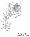
- As shown in Fig. 4, the
bonding head 1 comprises awire reel 3 mounted to awire reel mount 2 and abonding mechanism 10 for carrying out bonding operation with a wire 4, which is fed from thewire reel 3 located above, to a bonding object such as an IC chip or a wafer placed on the bonding stage (not shown). Also provided between thewire reel 3 and thebonding mechanism 10 are afirst wire tensioner 7 for applying an upward blow of air 6 to a midway portion of the wire 4 to cause the wire 4 to be curved upwardly and a second wire tensioner 9 for exposing the wire 4 to an upward blow of air 8 just above awire guide 11a of aclamper 11 in thebonding mechanism 10 to tension the wire 4 upwardly. Accordingly, the wire 4 drawn from thewire reel 3 can constantly be fed into thebonding mechanism 10 while being floated under proper tension through a prescribed feeding path by the blows of air 6 and 8. - Referring to Figs. 4 and 5, the
bonding mechanism 10 comprises theclamper 11 for securely holding'the wire 4, ahorn 13 provided with a capillary 12, through a distal end of which the wire 4 is passed, for applying ultrasonic vibration via thecapillary 12 to a ball 5 (Fig. 6) developed from a leading end of the wire 4, and atorch 14 for forming theball 5 with electric discharge. Amonitor camera 15 is provided above for visually monitoring the bonding operation, which displays a monitoring image on a monitor display (not shown), and delivers a monitor signal to a data processor (not shown) where it is processed. - The
clamper 11 and thehorn 13 are mounted to aswing member 16 for upward and downward swing movements about an unshown pivot. Theswing member 16 is driven to swing by a vertical motionelectromagnetic driver 17 for causing integral vertical movements of theclamper 11 and thehorn 13. Also, an open/closeelectromagnetic driver 18 is provided for opening and closing theclamper 11. - The bonding operation of the above arrangement will now be explained referring to Fig. 6. While the
clamper 11 and thecapillary 12 are located at their initial levels with the leading end of the wire 4 extending a given length from the lower end of thecapillary 12, thetorch 14 is activated to produce a spark current in synchronism with the movement of thebonding head 1 to a location where it comes opposite to atarget electrode 19 on anIC chip 20 so that the leading end of the wire 4 is melted to form aball 5 such as shown in Fig. 6(a). The opposite relationship between the wire 4 and theelectrode 19 is monitored and controlled precisely with visual recognition by themonitor camera 15. - The
swing member 16 is then driven by the vertical motionelectromagnetic driver 17 for causing theclamper 11 and thecapillary 12 to descend towards theIC chip 20 placed on the bonding stage (not shown). When the capillary 12 presses down theball 5 of the wire 4 against theelectrode 19 on theIC chip 20, as shown in Fig. 6(b), thehorn 13 applies ultrasonic vibration via thecapillary 12 to theball 5 which is thus bonded to theelectrode 19 by thermal compression and ultrasonic vibration. It is preferable to set the compression force within the range of 30 to 50 g (1g-force = 9.8 x 10⁻³ N) and the ultrasonic vibration, which is applied in a horizontal direction, to be 0.5 micrometer in amplitude and 60 to 70 kHz (specifically 63.5 kHz) in frequency. - During the bonding operation, the
clamper 11 is opened by the open/closeelectromagnetic driver 18 and lifted up together with the capillary 12 to a prescribed level by the vertical motionelectromagnetic driver 17. Accordingly, the wire 4 is extended from the lower end of thecapillary 12 by a certain length as shown in Fig. 6(c). - The
clamper 11 is then closed by the open/closeelectromagnetic driver 18 to hold the wire 4 securely, after which theswing member 16 is driven by the vertical motionelectromagnetic driver 17 to cause theclamper 11 and thecapillary 12 to move upwards as shown in Fig. 6(d) to their initial level shown in Fig. 6(a). In an early stage of this step, the wire 4 is separated at a boundary of heat effect hence leaving on the electrode 19 abump 21 of about 60 micrometers high which consists of aball portion 21a and a wire portion 21b of 30 to 40 micrometers high. - Since the above-described conventional bump forming method includes the step of drawing out the wire 4 shown in Fig. 6(c), which requires substantially 0.02 second, the cycle of bump forming operation from the start of action until it is returned to the initial state takes a total of about 0.1 second, because of which productivity cannot be further improved.
- US-A-4 925 083 discloses a further bump bonding operation.
- It is thus an object of the present invention to provide a bump forming method with which the time required for the cycle of bump forming operation can be reduced to thereby improve the productivity.
- A method of forming a bump according to the present invention is defined in
claim 1. - As the capillary and the clamper are lifted up and down separately, their lowermost locations in the second step are different from each other. This allows the wire to be separated from the finished bump as well as extended from the lower end of the capillary to provide another leading extension while the capillary and the clamper are being lifted up in the fourth step. Accordingly, a step of drawing out the wire which is necessary in the conventional method is eliminated and the cycle duration for forming a bump will successfully be decreased thus remarkably improving the productivity.
- A bump bonder suitable for carrying out the bump forming method according to the present invention is provided with a capillary for bonding a ball developed from a leading end of a wire; a clamper for securely holding the wire above the capillary; a horn having the capillary at the distal end thereof; supporting means for supporting a horn such as to allow the horn to move upwards and downwards, a driver for driving upward and downward movements of the horn; supporting means for supporting the clamper independently of the horn for upward and downward movements; and a driver for driving the clamper to move upward and downward.
- By this arrangement, since the means for lifting up and down the horn and the clamper are provided separately, the above described bump forming method can be implemented with the addition of a simple mechanism to the conventional construction.
-
- Fig. 1 is a perspective view showing a primary arrangement of a bonding head in a bump bonder which may be used to carry out the method of the present invention;
- Fig. 2 is a side view showing the primary arrangement of the bonding head;
- Fig. 3 is an explanatory view showing a series of bonding steps according to the invention;
- Fig. 4 is a perspective view of a wire feeder mechanism in a conventional bonding head;
- Fig. 5 is a perspective view of a primary arrangement of the conventional bonding head; and
- Fig. 6 is an explanatory view showing a series of bonding steps in the conventional bonding head.
-
- The bonding head in the bump bonder which may be used to carry out the method according to the present invention will be hereinafter described in more detail referring to Figs. 1 to 3. Since a wire feeder mechanism of the bonding head is identical to the one shown in Fig. 4, its description is omitted while the other constructions will be explained. Also, like elements are denoted by the same numerals as those shown in Fig. 5 and will be explained in no more detail.
- Referring to Figs. 1 and 2, the bonding head denoted by
reference numeral 1 is mounted on an XY table (not shown) which is movable in both X and Y directions for positioning thehead 1. The bondinghead 1 is located behind abonding stage 36 which includes a heating means for ultrasonic thermal compression bonding. - A
bonding mechanism 10 is provided for bonding an object or anIC chip 20 placed on thebonding stage 36, and a length of wire 4 is supplied from a wire reel (not shown) to thebonding mechanism 10. Thebonding mechanism 10 comprises aclamper 11 for holding the wire 4, a capillary 12 through which the wire 4 is passed at its distal end, ahorn 13 for applying ultrasonic vibration to aball 5 of the wire 4 via thecapillary 12, and atorch 14 for producing electric discharge. Amonitor camera 15 is mounted above for visually monitoring the bonding action and its image output is displayed on amonitor display 32 and transmitted as a monitor signal to adata processor 34 for data processing. - The
clamper 11 is mounted to the front of anupper swing member 22 which is supported by ahorizontal pivot 23 for upward and downward swing motions. A clamper vertical motionelectromagnetic driver 24 is provided just behind thehorizontal pivot 23 and aclamper position detector 25 is provided at the rear end of theupper swing member 22. Also provided are avertical pivot 26 which supports a middle portion of theclamper 11 for opening and closing actions, and an open/closeelectromagnetic driver 18 mounted behind theclamper 11. Thehorn 13 is mounted to the front end of alower swing member 27 which is supported by ahorizontal pivot 28 for upward and downward swing motions. A horn vertical motionelectromagnetic driver 29 is provided just behind thehorizontal pivot 28 and ahorn position detector 30 is provided at the rear end of thelower swing member 27. - The bonding operation with the above described arrangement is now explained referring to Fig. 3. In the initial state, the
clamper 11 and the capillary 12 are positioned at a predetermined height and are spaced by a certain distance A from each other, and the wire 4 is protruded from the distal end of thecapillary 12 by a given length. In this state, each time thebonding head 1 is moved to a location which is opposite to atarget electrode 19 on theIC chip 20, the distal end of the wire 4 is melted by a spark current from thetorch 14 so that aball 5 such as shown in Fig. 3(a) is formed. The positional relationship between the wire 4 and thetarget electrode 19 opposite to each other is visually monitored by themonitor camera 15 and thus can be controlled precisely. - Next, the
clamper 11 is opened, after which the clamper vertical motionelectromagnetic driver 24 and the horn vertical motionelectromagnetic driver 29 are activated to swing theupper swing member 22 and thelower swing member 27 respectively, so as to bring theclamper 11 and thecapillary 12 down towards theIC chip 20 placed on thebonding stage 36. In particular, theclamper 11 is lowered by a shorter distance which is equivalent to the length D of the wire 4 extended from the distal end of thecapillary 12 than thecapillary 12, so that theclamper 11 and thecapillary 12 will be spaced by the distance (A+D) at the lowermost end. After descending to the lowermost end, the capillary 12 compresses theball 5 of the wire 4 against theelectrode 19 of theIC chip 20 as shown in Fig. 3(b) and ultrasonic vibration is applied via thecapillary 12 by thehorn 13, as a result of which theball 5 and theelectrode 19 are joined to each other through thermal compression and ultrasonic vibration. The compression force may preferably be set from 30 to 50 g and the ultrasonic vibration, which is applied in a horizontal direction, may be 0.5 micrometer in amplitude and 60 to 70 kHz in frequency (most preferably, 63.5 kHz). - During the bonding operation, the open/close
electromagnetic driver 18 is activated to close theclamper 11 for securely holding the wire 4. After the bonding is completed, the clamper vertical motionelectromagnetic driver 24 and the horn vertical motionelectromagnetic driver 29 are activated to lift up theclamper 11 and thecapillary 12. In an early stage of this ascending step, the wire 4 is separated at a boundary portion of heat effect as shown in Fig. 3(c), hence producing on the electrode 19 abump 21 of about 60 micrometers high which consists of aball portion 21a and a wire portion 21b extending 30 to 40 micrometers long. When theclamper 11 and the capillary 12 are lifted up after that, the lowermost end of the wire 4 is drawn out downwardly from the distal end of the capillary 12 as shown in Fig. 3(d) due to a difference in the amount of movement between theclamper 11 and the capillary 12. As theclamper 11 and the capillary 12 are returned to their initial levels shown in Fig. 3(a), the difference D in the amount of movement between the two permits a given length of the wire 4 to protrude from the lower end of the capillary 12. - The bump bonder which may be used to carry out the method of the present invention further includes a vertical motion data unit (Fig. 2) for saving various kinds of data for controlling the upward and downward movements of the
clamper 11 and thehorn 13. More specifically, the amount of feeding the wire 4 may be preliminarily determined according to a desired form of the bump, types of wire or capillary, or to any other data which are saved in the data unit, based on which the respective upward and downward movements of theclamper 11 and thehorn 13 may be controlled. - During a cycle of the above bump forming operation, the step of lifting up the capillary by a certain distance before closing the clamper so as to draw out the wire 4 a predetermined length from the distal end of the capillary, which is included in the conventional method, is omitted, and the duration required for this step which is 0.02 second is thus eliminated, decreasing the whole duration of one cycle of bump forming operation to 0.08 second. Accordingly, the bump forming duration can be reduced by 20% only by providing
respective swing members electromagnetic drivers clamper 11 and thehorn 13, whereby a remarkable improvement in productivity can be achieved. - As set forth above, according to the present invention, the cycle of forming a bump is decreased. The invention is thus useful in the wire bonding technology where bumps for electric connection are formed on electrodes of an IC chip.
Claims (2)
- A method of forming a bump comprising:a first step of providing a distal end of a wire (4) to be protruding from a lower end of a capillary (12) by a predetermined length, a clamper (11) for securely holding the wire being located a distance above said capillary, and forming a ball (5) from the protruded portion of the wire (4);a second step of opening said clamper (11) and bringing down the capillary (12) as well as the clamper (11), in which an amount of movement of the clamper (11) is smaller than that of the capillary '(12) by such an amount as to be equivalent to said predetermined length of the wire (4) being protruded from the lower end of the capillary (12) before forming the ball (5) in the first step;a third step of forming a bump (21) from'the ball (5) by bonding; anda fourth step of separating the wire (4) from the bump (21) by closing the clamper (11) and lifting up the clamper (11) and the capillary (12) to the initial position of the first step as well as causing a distal end of the wire (4) to protrude from the lower end of the capillary (12) by said predetermined length.
- The method of forming a bump according to claim 1, wherein upward and downward movements of the clamper (11) and the capillary (12) are controlled based on a predetermined amount of feeding the wire (4) which is preliminarily set according to the desired form of the bump (21) or to the types of the wire (4) or the capillary (12).
Applications Claiming Priority (3)
| Application Number | Priority Date | Filing Date | Title |
|---|---|---|---|
| JP13391797 | 1997-05-23 | ||
| JP13391797 | 1997-05-23 | ||
| PCT/JP1998/002253 WO1998053485A1 (en) | 1997-05-23 | 1998-05-21 | Bump forming method and bump bonder |
Publications (2)
| Publication Number | Publication Date |
|---|---|
| EP0983607A1 EP0983607A1 (en) | 2000-03-08 |
| EP0983607B1 true EP0983607B1 (en) | 2002-07-24 |
Family
ID=15116116
Family Applications (1)
| Application Number | Title | Priority Date | Filing Date |
|---|---|---|---|
| EP98921766A Expired - Lifetime EP0983607B1 (en) | 1997-05-23 | 1998-05-21 | Bump forming method and bump bonder |
Country Status (5)
| Country | Link |
|---|---|
| US (1) | US6098868A (en) |
| EP (1) | EP0983607B1 (en) |
| KR (1) | KR100465552B1 (en) |
| DE (1) | DE69806754T2 (en) |
| WO (1) | WO1998053485A1 (en) |
Families Citing this family (16)
| Publication number | Priority date | Publication date | Assignee | Title |
|---|---|---|---|---|
| US6165888A (en) * | 1997-10-02 | 2000-12-26 | Motorola, Inc. | Two step wire bond process |
| DE19812706A1 (en) * | 1998-03-23 | 1999-10-07 | F&K Delvotec Bondtechnik Gmbh | Method and device for "ball-bonding" |
| JP2000133672A (en) | 1998-10-28 | 2000-05-12 | Seiko Epson Corp | Semiconductor device and its manufacturing method, circuit board, and electronic equipment |
| JP3407275B2 (en) * | 1998-10-28 | 2003-05-19 | インターナショナル・ビジネス・マシーンズ・コーポレーション | Bump and method of forming the same |
| EP1174908A1 (en) * | 2000-07-21 | 2002-01-23 | Esec Trading S.A. | Apparatus for making wire connections |
| DE10133885A1 (en) | 2000-07-21 | 2002-03-21 | Esec Trading Sa | Device for producing wire connections |
| EP1174906A1 (en) * | 2000-07-21 | 2002-01-23 | Esec Trading S.A. | Apparatus for making wire connections |
| US6471116B2 (en) * | 2001-01-19 | 2002-10-29 | Orthodyne Electronics Corporation | Wire bonding spool system |
| US6712261B2 (en) * | 2002-03-20 | 2004-03-30 | International Business Machines Corporation | Solid conductive element insertion apparatus |
| JP3727616B2 (en) * | 2002-07-11 | 2005-12-14 | 株式会社新川 | Wire bonding equipment |
| JP2005251919A (en) * | 2004-03-03 | 2005-09-15 | Shinkawa Ltd | Bump bonding apparatus and bump non-stick detection method |
| US7863737B2 (en) * | 2006-04-01 | 2011-01-04 | Stats Chippac Ltd. | Integrated circuit package system with wire bond pattern |
| MY149251A (en) * | 2008-10-23 | 2013-07-31 | Carsem M Sdn Bhd | Wafer-level package using stud bump coated with solder |
| US8459530B2 (en) * | 2009-10-29 | 2013-06-11 | Asm Technology Singapore Pte Ltd | Automatic wire feeding method for wire bonders |
| US8919632B2 (en) * | 2012-11-09 | 2014-12-30 | Asm Technology Singapore Pte. Ltd. | Method of detecting wire bonding failures |
| CN105895543B (en) * | 2014-12-01 | 2019-09-13 | 恩智浦美国有限公司 | Bonding wire feeding system and method thereof |
Family Cites Families (12)
| Publication number | Priority date | Publication date | Assignee | Title |
|---|---|---|---|---|
| GB2201545B (en) * | 1987-01-30 | 1991-09-11 | Tanaka Electronics Ind | Method for connecting semiconductor material |
| DE3703694A1 (en) * | 1987-02-06 | 1988-08-18 | Dynapert Delvotec Gmbh | BALL BONDING METHOD AND DEVICE FOR CARRYING OUT THE SAME |
| JPH03208354A (en) * | 1990-01-10 | 1991-09-11 | Mitsubishi Electric Corp | Semiconductor device and manufacture thereof |
| JPH04247631A (en) * | 1991-02-01 | 1992-09-03 | Mitsubishi Electric Corp | Wire bonder |
| JP2841126B2 (en) * | 1991-04-19 | 1998-12-24 | 株式会社新川 | Wire bonding method and apparatus |
| US5326015A (en) * | 1993-03-29 | 1994-07-05 | Kulicke And Soffa Investments, Inc. | Wire bonder tail length monitor |
| JPH08249724A (en) * | 1995-03-10 | 1996-09-27 | Ricoh Co Ltd | Phase change type optical memory medium and manufacturing method thereof |
| JP3218382B2 (en) * | 1995-12-05 | 2001-10-15 | 株式会社新川 | Wire bonding method of coated wire |
| JP3074517B2 (en) * | 1995-12-05 | 2000-08-07 | 株式会社新川 | Wire bonding method of coated wire |
| JP3082657B2 (en) * | 1996-02-08 | 2000-08-28 | 松下電器産業株式会社 | Bump forming apparatus and bump forming method |
| JPH09252005A (en) * | 1996-03-15 | 1997-09-22 | Shinkawa Ltd | Bump forming method |
| JP3400279B2 (en) * | 1997-01-13 | 2003-04-28 | 株式会社新川 | Bump forming method |
-
1998
- 1998-05-12 US US09/423,375 patent/US6098868A/en not_active Expired - Fee Related
- 1998-05-21 WO PCT/JP1998/002253 patent/WO1998053485A1/en not_active Ceased
- 1998-05-21 KR KR10-1999-7010838A patent/KR100465552B1/en not_active Expired - Fee Related
- 1998-05-21 EP EP98921766A patent/EP0983607B1/en not_active Expired - Lifetime
- 1998-05-21 DE DE69806754T patent/DE69806754T2/en not_active Expired - Fee Related
Also Published As
| Publication number | Publication date |
|---|---|
| EP0983607A1 (en) | 2000-03-08 |
| DE69806754T2 (en) | 2003-10-16 |
| WO1998053485A1 (en) | 1998-11-26 |
| US6098868A (en) | 2000-08-08 |
| KR20010012872A (en) | 2001-02-26 |
| KR100465552B1 (en) | 2005-01-13 |
| DE69806754D1 (en) | 2002-08-29 |
Similar Documents
| Publication | Publication Date | Title |
|---|---|---|
| US6098868A (en) | Bump forming method and bump bonder | |
| TWI397138B (en) | Wire bonding method, wire bonding device, and wire bonding control program | |
| EP1422014B1 (en) | Semiconductor device having a wire loop with a crushed part on a ball, loop wire bonding method and loop wire bonding apparatus for carrying out such method | |
| US7584881B2 (en) | Low loop height ball bonding method and apparatus | |
| KR100283501B1 (en) | Semiconductor device and manufacturing method thereof and semiconductor device and manufacturing method thereof | |
| US20050199677A1 (en) | Wire bonding apparatus having actuated flame-off wand | |
| JP2723277B2 (en) | Wire bonding method | |
| JP3615934B2 (en) | Bump forming method and bump bonder | |
| CN100449720C (en) | Wire bonding method | |
| US20240006193A1 (en) | Semiconductor device manufacturing method and manufacturing apparatus | |
| US20060011710A1 (en) | Formation of a wire bond with enhanced pull | |
| JP3124653B2 (en) | Wire bonding method | |
| JP2885242B1 (en) | Wire bonding method and apparatus | |
| JP3754538B2 (en) | Bonding method and bump bonder | |
| JPH06132344A (en) | Wire bonding equipment | |
| JP2000036512A (en) | Wire bonding apparatus, wire bonding method, and capillary used in the wire bonding apparatus or wire bonding method | |
| JPS62179733A (en) | Wire bonding system | |
| JPH03263844A (en) | Insertion of wire into capillary in wire bonder | |
| JPH0831459B2 (en) | Ball bump forming method and apparatus | |
| JP3642918B2 (en) | Bump bonder | |
| CN118720531A (en) | Wire welding machine with winding function and automatic wire winding welding method | |
| JP3417659B2 (en) | Wire bonding equipment | |
| JP2586679B2 (en) | Wire bonding method | |
| JPS6248033A (en) | Wire bonding method | |
| JPS636849A (en) | Wire bonding |
Legal Events
| Date | Code | Title | Description |
|---|---|---|---|
| PUAI | Public reference made under article 153(3) epc to a published international application that has entered the european phase |
Free format text: ORIGINAL CODE: 0009012 |
|
| 17P | Request for examination filed |
Effective date: 19991215 |
|
| AK | Designated contracting states |
Kind code of ref document: A1 Designated state(s): DE FR GB |
|
| GRAG | Despatch of communication of intention to grant |
Free format text: ORIGINAL CODE: EPIDOS AGRA |
|
| 17Q | First examination report despatched |
Effective date: 20010918 |
|
| GRAG | Despatch of communication of intention to grant |
Free format text: ORIGINAL CODE: EPIDOS AGRA |
|
| GRAH | Despatch of communication of intention to grant a patent |
Free format text: ORIGINAL CODE: EPIDOS IGRA |
|
| GRAH | Despatch of communication of intention to grant a patent |
Free format text: ORIGINAL CODE: EPIDOS IGRA |
|
| GRAA | (expected) grant |
Free format text: ORIGINAL CODE: 0009210 |
|
| AK | Designated contracting states |
Kind code of ref document: B1 Designated state(s): DE FR GB |
|
| REG | Reference to a national code |
Ref country code: GB Ref legal event code: FG4D |
|
| REF | Corresponds to: |
Ref document number: 69806754 Country of ref document: DE Date of ref document: 20020829 |
|
| ET | Fr: translation filed | ||
| PLBE | No opposition filed within time limit |
Free format text: ORIGINAL CODE: 0009261 |
|
| STAA | Information on the status of an ep patent application or granted ep patent |
Free format text: STATUS: NO OPPOSITION FILED WITHIN TIME LIMIT |
|
| 26N | No opposition filed |
Effective date: 20030425 |
|
| PGFP | Annual fee paid to national office [announced via postgrant information from national office to epo] |
Ref country code: FR Payment date: 20070510 Year of fee payment: 10 |
|
| PGFP | Annual fee paid to national office [announced via postgrant information from national office to epo] |
Ref country code: DE Payment date: 20080529 Year of fee payment: 11 |
|
| PGFP | Annual fee paid to national office [announced via postgrant information from national office to epo] |
Ref country code: GB Payment date: 20080521 Year of fee payment: 11 |
|
| REG | Reference to a national code |
Ref country code: FR Ref legal event code: ST Effective date: 20090119 |
|
| PG25 | Lapsed in a contracting state [announced via postgrant information from national office to epo] |
Ref country code: FR Free format text: LAPSE BECAUSE OF NON-PAYMENT OF DUE FEES Effective date: 20080602 |
|
| GBPC | Gb: european patent ceased through non-payment of renewal fee |
Effective date: 20090521 |
|
| PG25 | Lapsed in a contracting state [announced via postgrant information from national office to epo] |
Ref country code: GB Free format text: LAPSE BECAUSE OF NON-PAYMENT OF DUE FEES Effective date: 20090521 |
|
| PG25 | Lapsed in a contracting state [announced via postgrant information from national office to epo] |
Ref country code: DE Free format text: LAPSE BECAUSE OF NON-PAYMENT OF DUE FEES Effective date: 20091201 |