EP0978880B1 - Panneau d'affichage électroluminescent en matière organique et procédé pour sa fabrication - Google Patents
Panneau d'affichage électroluminescent en matière organique et procédé pour sa fabrication Download PDFInfo
- Publication number
- EP0978880B1 EP0978880B1 EP98306353A EP98306353A EP0978880B1 EP 0978880 B1 EP0978880 B1 EP 0978880B1 EP 98306353 A EP98306353 A EP 98306353A EP 98306353 A EP98306353 A EP 98306353A EP 0978880 B1 EP0978880 B1 EP 0978880B1
- Authority
- EP
- European Patent Office
- Prior art keywords
- electrodes
- electrode
- organic
- bus
- display panel
- Prior art date
- Legal status (The legal status is an assumption and is not a legal conclusion. Google has not performed a legal analysis and makes no representation as to the accuracy of the status listed.)
- Expired - Lifetime
Links
Images


Classifications
-
- H—ELECTRICITY
- H10—SEMICONDUCTOR DEVICES; ELECTRIC SOLID-STATE DEVICES NOT OTHERWISE PROVIDED FOR
- H10K—ORGANIC ELECTRIC SOLID-STATE DEVICES
- H10K59/00—Integrated devices, or assemblies of multiple devices, comprising at least one organic light-emitting element covered by group H10K50/00
- H10K59/10—OLED displays
- H10K59/17—Passive-matrix OLED displays
- H10K59/179—Interconnections, e.g. wiring lines or terminals
-
- H—ELECTRICITY
- H10—SEMICONDUCTOR DEVICES; ELECTRIC SOLID-STATE DEVICES NOT OTHERWISE PROVIDED FOR
- H10K—ORGANIC ELECTRIC SOLID-STATE DEVICES
- H10K59/00—Integrated devices, or assemblies of multiple devices, comprising at least one organic light-emitting element covered by group H10K50/00
- H10K59/10—OLED displays
- H10K59/18—Tiled displays
Definitions
- the present invention relates to an organic electroluminescent (hereinafter referred to as EL) display panel comprising organic EL elements which emit light when electric charges are injected to an emitting layer.
- EL organic electroluminescent
- Organic EL devices also called organic light emitting diodes (LEDs)
- LEDs organic light emitting diodes
- Organic EL devices are extremely thin, matrix-addressable and operable at a relatively low voltage, typically less than 15 volts.
- FPDs next generation flat panel displays
- a major drawback of liquid crystal display, currently most well-known display of choice, is that most of them require bright backlighting, which can be easily eliminated by the use of an organic EL display.
- Organic LEDs differ fundamentally from conventional inorganic LEDs. While the charge transfer in inorganics is band-like in nature and the electron-hole recombination results in the interband emission of light, organic films are generally characterized by the low-mobility activated hopping transport and the emission is excitonic. Organic EL devices are also substantially different from conventional inorganic EL devices, especially in that organic EL devices are operable at low DC voltages.
- the RC time delay is significant in an organic EL display due to somewhat poor conductivity of indium tin oxide (ITO), a typical material for transparent electrode, and relatively large capacitance component of organic layers. As the panel size increases, the time delay becomes prohibitively large. More importantly, an organic EL display element does not have an intrinsic memory and so needs a very high peak luminance for a passive matrix addressing, which limits the number of rows of the display panel. The instantaneous peak luminance is proportional to (number of row) x (average luminance). To achieve an average display luminance of 100 cd/m 2 , for example, the maximum number of rows will probably be limited to less than 500.
- ITO indium tin oxide
- the estimation is made with the assumption that a peak luminance is 50,000 cd/m 2 , which is not trivial to achieve, and the device stability will certainly be a critical issue at that high luminance.
- the instantaneously high current causes large IR potential drops along the column and row buses, which should contribute to the non-uniformity of brightness over the panel surface.
- a solution to the problems discussed above is to employ an active addressing scheme as in a thin film transistor liquid crystal display (TFT-LCD).
- TFT-LCD thin film transistor liquid crystal display
- AM-EL active matrix EL
- PDP plasma display panel
- WO 97/38445 EP 0 767 599 and JP 09102392 each disclose an organic electroluminescent display panel as set out in the precharacterizing portion of claim 1.
- US 5790216 describes first and second bus electrodes for subpanels of a LC-display.
- the present invention is directed to an organic electroluminescent display panel that substantially addresses one or more of the problems due to limitations and disadvantages discussed in the above.
- An object of the present invention is to provide a passive addressable organic electroluminescent display panel with a plurality of sub-panels and a method for manufacturing the same.
- the invention provides an organic electroluminescent display panel as set out in claim 1, and a method of making an organic electroluminescent display panel as set out in claim 7.
- Embodiments provide an organic electroluminescent display panel having a plurality of emitting portions comprising: a transparent substrate; a plurality of first electrodes formed on said transparent substrate, each first electrode made up of a plurality of stripes which are electrically isolated from each other, each stripe electrically connected to a first bus electrode made up of a single or a plurality of electrically conducting materials, each first bus electrode, if necessary, vertically stacked with an electrically insulating layer in between, each of said stacked layers made up of one or a plurality of first bus electrodes arranged side by side with an electrically insulating gap in between; organic function layers formed on said first electrodes, including at least one organic EL medium layer; and a plurality of second electrodes formed on said organic function layers, each second electrode made up of a plurality of stripes which are electrically isolated from each other, each stripe electrically connected to a second bus electrode made up of a single or a plurality of electrically conducting materials, each second bus electrode, if necessary, vertically stacked with
- the organic EL display panel may further comprise a plurality of ramparts formed on corresponding second signal buses.
- a corresponding second electrode is formed on each rampart.
- a corresponding said at least one of first, second and third organic function layers is formed between the corresponding second electrode and each rampart.
- the organic EL display panel may further comprise a rampart formed on a corresponding first signal bus located between adjacent sub-panels.
- each of said plurality of first and second electrodes comprises a plurality of first and second conductive layers, respectively, arranged in an array of columns and rows, each of said first and second conductive layers being isolated from each other.
- said plurality of first conductive layers is made of a light transmissive material.
- the light transmissive material is indium tin oxide.
- said substrate is light transmissive.
- said first conductive layers have a substantially rectangular shape.
- a corresponding first conductive layer in a corresponding sub-panel includes a plurality of notches on one side of the substantially rectangular shape.
- said plurality of second conductive layers is made of one of a low resistance metal and alloy.
- the low resistance metal is aluminium
- the alloy is one of Mg:Ag and Al:Li.
- said plurality of first signal buses is formed in a column direction between at least one of adjacent first conductive layers for coupling at a first side of a corresponding first conductive layer and corresponding first conductive layers for coupling at a second side, wherein the first and second sides are different sides of the first conductive layers.
- said plurality of second signal buses is formed in a row direction between at least one of adjacent second conductive layers for coupling at a first side of a corresponding second conductive layer and corresponding second conductive layer for coupling at a second side, wherein the first and second sides are different sides of the second conductive layers.
- each of said plurality of first signal buses comprises at least one conductive first connection formed on the substrate and a first insulating layer covering said conductive first connection and each of said plurality of second signal buses comprises a second insulation layer formed on the first conductive layer, at least one conductive second connection formed on the first conductive layer and a third insulation layer formed on the conductive second connection.
- each of said conductive first and second connections are made of at least one conductive material.
- the conductive material is at least one of a metal, an alloy and a conducting polymer.
- the metal is one of aluminum, copper, nickel, chromium, silver and gold.
- At least one of the conductive first connection is in contact with an entire first side of the corresponding first conductive layer and the conductive second connection is in contact with an entire first side of the corresponding second conductive layer.
- the first insulating layer isolates adjacent conductive first connections when there is more than one conductive first connection for each first signal bus and said third insulating layer isolates adjacent active second connections when there is more than one conductive connection for each second signal bus.
- At least one of the adjacent conductive first and second connections are vertically stacked.
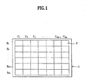
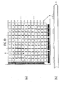
- Fig. 1 schematically illustrates a plan view of an organic EL display panel in accordance with a preferred embodiment of the present invention.
- the organic EL display panel 1 has a large viewing area which is divided into sub-panels 2 of (2m x 2n), i.e. columns of 2m and rows of 2n. wherein m and n are integers greater than 2. Each sub-panel will be electrically driven separately to obviate the problems associated with a passive addressing of a large panel.
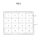
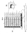
- Fig. 2 shows specifically a display panel having (4 x 4) sub-panels.
- the panel 1 has an active viewing area which is constituted of sixteen sub-panels 2.
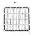
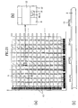
- a series of fabrication steps devised in the present invention have been illustrated in Figs. 3 ⁇ 14 for an exemplary display panel having (4 x 4) sub-panels.
- Said first electrode is apparently different from an anode used in a typical matrix addressing in that each first electrode is divided into 4 stripes.
- Each stripe of an electrode is electrically isolated from others, which can be utilized to drive each sub-panel 2 of the display panel separately.
- Fig. 3 also shows a plurality of contact pads 5 & 6 for first and second electrodes, respectively, formed on the transparent substrate. Said contact pads may be formed simultaneously during the formation of first electrodes.
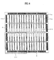
- first bus electrodes 7-b which are formed preferably of a highly conductive metal such as aluminum or its alloys.
- first bus electrodes 7-b There are several different ways to form said first bus electrodes 7-b, and a preferred method is to form the bus electrode only on the selective position using a lift-off process.
- the film growth may be performed using any of vapor deposition, e-beam evaporation.
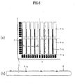
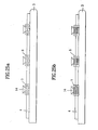
- Fig. 5(a) is a close-up view of four sub-panels designated as 2-f in Fig. 4
- Fig. 5(b) illustrates a cross-sectional view taken along the line A-A' in Fig. 5(a) .
- IR potential drops along a long side of each rectangular-shaped stripe of first electrodes can be significantly reduced by increasing the contact area between each of first bus electrodes and a corresponding stripe of first electrodes, which thereby makes a contribution towards a uniform emission of a sub-panel.
- said first bus electrode serves as an auxiliary electrode for a stripe of first electrode because the electrical resistance of ITO, typically used for a first electrode, is much larger than that of a metal used for a bus electrode.
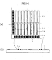
- a preferred way is to form each bus electrode along a long side of corresponding rectangular-shaped stripe, as shown in Fig. 5-1 , making the two in electrical contact over the entire length of a long side of said stripe or over a substantial fraction of the whole length of said long side. Said contacts can be either continuous or evenly distributed lengthwise along the long side of said stripe.
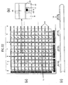
- a layer of electrically insulating material(s) is formed on top of said first bus electrodes 7-b (see Fig. 6 ).
- Said layer 8 is required to be mechanically and chemically stable, and may be made of organic or inorganic insulating material(s).
- Preferred materials are inorganic compounds such as silicon oxide and silicon nitride, and the film growth may be performed using any of vapor deposition, e-beam evaporation, RF sputtering, chemical vapor deposition (CVD), spin coating, dipping, Dr. blade method, electro- and electroless platings, and screen printing method.
- Fig. 7(a) is a schematic view illustrating the process of forming an insulating buffer layer on top of which second bus electrodes are to be formed orthogonal to first bus electrodes in the following step.
- the role of said buffer layer 9 is to electrically isolate second bus electrodes from first electrodes.
- the materials and film growth methods used to form said buffer layer are basically the same as those for the insulating layer 8 in Fig. 6 .
- Said buffer layer may be formed together with the insulating layer 8 in the previous step (see Fig. 7-1 ).
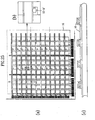
- second bus electrodes are formed to be orthogonal to first bus electrodes, as shown in Fig. 8 .
- the role of said bus electrodes is to electrically connect contact pads 6 and second electrodes which are to be formed in the next process.
- the short connections 10-a may be omitted, depending on the structural design employed.
- the long connections 10-b are formed mostly on top of the insulating layer 9, and, as shown in Fig. 8(b) , a part of said bus electrode (10-b') is formed on an open area 11 which is not covered with the first electrode layer 4 (ITO) unlike the area 12.
- Second bus electrodes can be formed using the same materials and film growth methods as for first bus electrodes.
- an insulating layer is formed on top of said second bus electrodes as in Fig. 9 .
- said insulating layer 13 may be omitted.
- the materials and fabrication methods of said insulating layer are basically the same as those described earlier.
- second bus electrodes may be formed before first bus electrodes.
- next processing steps may vary substantially.
- next processing steps may vary substantially.
- a series of organic function materials are to be simply laminated.
- additional shadow mask(s) may be required for the construction of a multi or full color display: (1) putting a shadow mask onto top surfaces of the ramparts, the shadow mask having a plurality of openings each exposing one of either first or second electrodes, whichever suitable, between said ramparts, and aligning the openings to said electrodes respectively; (2) depositing first organic EL media through said openings onto said electrodes between said ramparts respectively, thereby forming first (R) organic function layers; (3) after realigning the shadow mask, repeating the process (2) to form second (G) and third (B) organic function layers; and (4) forming at least one second electrode on said ramparts and said organic function layers.
- Fig. 10 illustrates the process of forming electrically insulating ramparts for pixelation as described in the above.
- Said ramparts 14 are formed on top of the insulating layer 13 which serves as a buffer layer here.
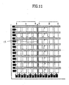
- An additional rampart 15 is required to electrically isolate second electrodes in A region from those in B region as illustrated in Fig. 11 .
- An exemplary green-emitting device may have organic function layers of: (1) a hole injecting buffer layer of copper phthalocyanine (CuPc) typically 10nm ⁇ 20nm thick, (2) a hole transporting layer of N,N'-diphenyl-N,N'-bis(3-methylphenyl)-(1,1'-biphenyl)-4,4'-diamine (TPD) typically 30nm - 50nm thick, and (3) an emitting layer of tris(8-hydroxy-quinolate)aluminum (Alq 3 ) 40nm ⁇ 60nm thick which is often doped with a fraction of an emitting dye such as coumarin 6 or quinacridone.
- One of the preferred methods to fabricate a full color display panel is to laminate each of red, green and blue emitting materials onto the corresponding pixels step by step using a plurality of ramparts and shadow mask(s), as described earlier.
- Fig. 13 illustrates the process of exposing a part of second bus electrode 10-b' by etching out organic function layers deposited right on top of said bus electrode 10-b' for the purpose of making an electrical contact between said bus electrode and the second electrode layer which is to be deposited in the following step ( Fig. 14 ).
- the etching can be accomplished preferably using a dry etching process such as reactive ion etching or laser etching.
- Figures show, for clarity, only one window for electrical contact per each of second bus electrodes, but the number of said contact windows or connection pads may be increased to, for example, one per each pixel, if necessary.
- one contact window per each bus electrode is sufficient because the material for a second electrode (Al, or Al:Li) generally has much lower resistivity compared to that for a first electrode (ITO).
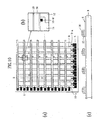
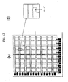
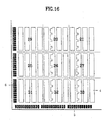
- the exemplary fabrication processes described for (4 x 4) sub-panels are applicable to the fabrication of an even larger panel of (6 x 6) sub-panels as shown in Fig. 15 . Due to the symmetry involved, description with respect to only (3 x 3) sub-panels ( fig. 16 ) should be sufficient to elucidate the fabrication steps of (6 x 6) sub-panels.
- the illustrations of Figs 17 - 24 concern the processing steps for said panel with (3 x 3) sub-panels, which are basically the same as those for (4 x 4) described already. But there are several differences as follows. As seen in Fig. 17 , it is necessary to form one more bus electrodes per each first electrode compared to (4 x 4).
- Fig. 20 shows again the presence of one more bus electrodes per each second electrode compared to (4 x 4), i.e. 10-a, 10-b and 10-c.
- Fig. 25 is a perspective view describing the intersections of first and second bus electrodes.
- Each of the sub-panels fabricated as described above can be driven using a driving circuitry which is separate, but not completely independent from the remaining circuitry. Separate driving here means that each sub-panel has separate scan and data lines which should be properly synchronized with the remaining circuitry.
- the organic EL devices have the following advantages.
- Effective driving of a large organic EL display panel has been made possible by forming a plurality of stripes for each of first electrodes and also for each of second electrodes. These stripes are electrically isolated from each other, which enables each group of pixels defined by a set of orthogonal stripes to be driven separately from the remaining groups of pixels. Efficient fabrication methods devised to construct said display panel are cost effective and suitable for mass production.
Landscapes
- Electroluminescent Light Sources (AREA)
- Devices For Indicating Variable Information By Combining Individual Elements (AREA)
Claims (10)
- Panneau d'affichage électroluminescent organique (1) à adressage passif comprenant :une pluralité de premières électrodes (4), et une pluralité de secondes électrodes (17), orthogonales auxdites premières électrodes, formant une matrice de colonnes et de lignes ; etune pluralité de parties émettant de la lumière (16) stratifiées entre les premières et secondes électrodes ;caractérisé en ce que :la matrice d'électrodes est divisée en m x n sous-panneaux (2) électriquement attaquables séparément, où m et n sont des entiers supérieurs à 2 ;chaque première électrode (4) est composée de m bandes conductrices isolées électriquement les unes des autres, agencées de sorte que chaque bande conductrice attaque des parties émettant de la lumière d'un sous-panneau différent parmi les sous-panneaux le long de la direction de longueur de la première électrode ;chaque seconde électrode (17) est composée de n bandes conductrices isolées électriquement les unes des autres, agencées de sorte que chaque bande conductrice attaque des parties émettant de la lumière d'un sous-panneau différent parmi les sous-panneaux le long de la direction de longueur de la seconde électrode ; etle panneau d'affichage comprend en outre un ensemble de circuits d'attaque séparé pour chaque sous-panneau (2), un substrat (3), ladite pluralité de premières électrodes (4) formées sur ledit substrat, une pluralité de premières électrodes bus (7-b) entre des premières électrodes adjacentes, et chaque bande de chacune de ladite pluralité de premières électrodes étant connectée électriquement à une première électrode bus respective (7-b) ;où une pluralité de secondes électrodes bus (10-b) sont formées en lignes orthogonalement auxdites premières électrodes bus et sur celles-ci et isolées dudit substrat (3) pour exposer au moins des parties des premières électrodes respectivement ; etla partie émettant de la lumière est formée d'au moins une couche parmi une première, une seconde et une troisième couches à fonction organique (16) formées sur lesdites parties exposées desdites premières électrodes (4), chacune desdites couches à fonction organique comportant au moins une couche de milieu électroluminescent organique, ladite pluralité de secondes électrodes (17) formées sur lesdites couches à fonction organique (16) et chaque bande de chacune de ladite pluralité de secondes électrodes étant connectée électriquement à une seconde électrode bus (10-b) respective ;où l'extrémité de la seconde électrode bus est couplée à une seconde bande d'électrode correspondante par le biais d'une ouverture formée dans l'une des première, seconde et troisième couches à fonction organique.
- Panneau d'affichage électroluminescent organique de la revendication 1, dans lequel chacune desdites premières et secondes électrodes bus (7-b, 10-b) comprend une partie d'une structure multicouches empilées à la verticale avec une couche électriquement isolante au milieu, chacune desdites structure multicouches empilées à la verticale comprend l'une de ladite pluralité de premières et secondes électrodes bus (7-b, 10-b) agencées côte-à-côte avec un jeu électriquement isolant au milieu.
- Panneau d'affichage électroluminescent organique de la revendication 1, dans lequel chaque bande conductrice desdites premières électrodes et une première électrode bus correspondante sont formées pour rester en contact électrique au niveau d'au moins un endroit.
- Panneau d'affichage électroluminescent organique de la revendication 1, dans lequel lesdites premières et secondes électrodes bus (7-b, 10-b) sont réalisées à partir d'au moins un matériau conducteur et ledit substrat est réalisé à partir d'un matériau transparent.
- Panneau d'affichage électroluminescent organique de la revendication 4, dans lequel ledit matériau électriquement conducteur consiste en au moins un matériau parmi des métaux, des alliages et des polymères conducteurs.
- Panneau d'affichage électroluminescent organique de la revendication 5, dans lequel ledit métal est l'un de l'aluminium, du cuivre, du nickel, du chrome, de l'argent et de l'or.
- Procédé de fabrication d'un panneau d'affichage électroluminescent organique à adressage passif comprenant les étapes qui consistent à :former une pluralité de premières électrodes (4) et une pluralité de secondes électrodes (17) en une matrice de colonnes et de lignes sur un substrat avec une pluralité de parties émettant de la lumière (16) stratifiées entre elles ;caractérisé en ce que :la matrice d'électrodes est divisée en m x n sous-panneaux (2) électriquement attaquables séparément, où m et n sont des entiers supérieurs à 2 ;chaque première électrode (4) est composée de m premières bandes conductrices isolées électriquement les unes des autres et agencées de sorte que chaque bande conductrice attaque des parties émettant de la lumière d'un sous-panneau différent parmi les sous-panneaux le long de la direction de longueur de la première électrode ;chaque seconde électrode (17) est composée de n secondes bandes conductrices isolées électriquement les unes des autres et agencées de sorte que chaque bande conductrice attaque des parties émettant de la lumière d'un sous-panneau différent parmi les sous-panneaux le long de la direction de longueur de la seconde électrode ; etcomprenant en outre le fait de prévoir un ensemble de circuits d'attaque séparé pour chaque sous-panneau (2) ;dans lequel l'étape consistant à former une pluralité de premières électrodes et une pluralité de secondes électrodes en une matrice avec une pluralité de parties émettant de la lumière stratifiées entre elles, comprend les étapes qui consistent à :après avoir formé les premières électrodes (4), former une pluralité de premières électrodes de bus de signaux (7-b) entre des premières électrodes adjacentes dans une direction de colonne et chacune des premières électrodes étant couplée à une bande correspondante des premières électrodes ;former une pluralité de secondes électrodes de bus de signaux (10-b) dans une direction de ligne et isolées du substrat pour exposer au moins des parties des premières électrodes, respectivement ;former au moins une couche parmi une première, une seconde et une troisième couches à fonction organique sur les parties exposées des premières électrodes (4), chacune desdites première, seconde et troisième couches à fonction organique comportant au moins un milieu électroluminescent organique ; etformer la pluralité de secondes électrodes (17) sur au moins une couche parmi une première, seconde et troisième couches à fonction organique et dont chaque bande est couplée à une seconde électrode de bus de signaux correspondante (10-b),où l'extrémité d'au moins une seconde électrode de bus de signaux est couplée à une seconde électrode correspondante par le biais d'une ouverture formée dans l'une des première, seconde et troisième couches à fonction organique.
- Procédé de la revendication 7, dans lequel l'extrémité de la seconde électrode de bus de signaux (10-b) est formée essentiellement perpendiculaire à la partie principale de la seconde électrode de bus de signaux.
- Procédé de la revendication 8, dans lequel ladite première bande conductrice a une forme essentiellement rectangulaire, et une pluralité d'encoches sont formées sur un côté des premières bandes conductrices.
- Procédé de la revendication 9, dans lequel chaque seconde électrode de bus de signaux fait saillie dans une région définie par une encoche correspondante.
Priority Applications (4)
| Application Number | Priority Date | Filing Date | Title |
|---|---|---|---|
| EP10005091.3A EP2234162B1 (fr) | 1998-08-07 | 1998-08-07 | Panneau d'affichage électroluminescent en matière organique et procédé pour sa fabrication |
| DE69841924T DE69841924D1 (de) | 1998-08-07 | 1998-08-07 | Organische Elektrolumineszenzanzeige und Verfahren zu deren Herstellung |
| EP98306353A EP0978880B1 (fr) | 1998-08-07 | 1998-08-07 | Panneau d'affichage électroluminescent en matière organique et procédé pour sa fabrication |
| HK00104745.0A HK1025665A1 (en) | 1998-08-07 | 2000-07-28 | Organic electroluminescent display panel and method for fabricating the same |
Applications Claiming Priority (1)
| Application Number | Priority Date | Filing Date | Title |
|---|---|---|---|
| EP98306353A EP0978880B1 (fr) | 1998-08-07 | 1998-08-07 | Panneau d'affichage électroluminescent en matière organique et procédé pour sa fabrication |
Related Child Applications (2)
| Application Number | Title | Priority Date | Filing Date |
|---|---|---|---|
| EP10005091.3A Division EP2234162B1 (fr) | 1998-08-07 | 1998-08-07 | Panneau d'affichage électroluminescent en matière organique et procédé pour sa fabrication |
| EP10005091.3 Division-Into | 2010-05-14 |
Publications (2)
| Publication Number | Publication Date |
|---|---|
| EP0978880A1 EP0978880A1 (fr) | 2000-02-09 |
| EP0978880B1 true EP0978880B1 (fr) | 2010-10-06 |
Family
ID=8234991
Family Applications (2)
| Application Number | Title | Priority Date | Filing Date |
|---|---|---|---|
| EP98306353A Expired - Lifetime EP0978880B1 (fr) | 1998-08-07 | 1998-08-07 | Panneau d'affichage électroluminescent en matière organique et procédé pour sa fabrication |
| EP10005091.3A Expired - Lifetime EP2234162B1 (fr) | 1998-08-07 | 1998-08-07 | Panneau d'affichage électroluminescent en matière organique et procédé pour sa fabrication |
Family Applications After (1)
| Application Number | Title | Priority Date | Filing Date |
|---|---|---|---|
| EP10005091.3A Expired - Lifetime EP2234162B1 (fr) | 1998-08-07 | 1998-08-07 | Panneau d'affichage électroluminescent en matière organique et procédé pour sa fabrication |
Country Status (3)
| Country | Link |
|---|---|
| EP (2) | EP0978880B1 (fr) |
| DE (1) | DE69841924D1 (fr) |
| HK (1) | HK1025665A1 (fr) |
Families Citing this family (5)
| Publication number | Priority date | Publication date | Assignee | Title |
|---|---|---|---|---|
| GB2371910A (en) | 2001-01-31 | 2002-08-07 | Seiko Epson Corp | Display devices |
| JP2008181986A (ja) * | 2007-01-24 | 2008-08-07 | Nippon Seiki Co Ltd | 有機elディスプレイ |
| AT505688A1 (de) * | 2007-09-13 | 2009-03-15 | Nanoident Technologies Ag | Sensormatrix aus halbleiterbauteilen |
| US8207954B2 (en) | 2008-11-17 | 2012-06-26 | Global Oled Technology Llc | Display device with chiplets and hybrid drive |
| US20110102413A1 (en) * | 2009-10-29 | 2011-05-05 | Hamer John W | Active matrix electroluminescent display with segmented electrode |
Citations (3)
| Publication number | Priority date | Publication date | Assignee | Title |
|---|---|---|---|---|
| EP0767599A2 (fr) * | 1995-10-06 | 1997-04-09 | Pioneer Electronic Corporation | Panneau d'affichage électroluminescent en matière organique et procédé pour sa fabrication |
| JPH09102392A (ja) * | 1995-10-06 | 1997-04-15 | Idemitsu Kosan Co Ltd | 有機elパネルおよびこのパネルを用いた表示装置 |
| US5790216A (en) * | 1993-11-28 | 1998-08-04 | Smartlight Ltd. | Viewing apparatus and work station |
Family Cites Families (8)
| Publication number | Priority date | Publication date | Assignee | Title |
|---|---|---|---|---|
| JPH02187787A (ja) * | 1989-01-13 | 1990-07-23 | Tokyo Electric Co Ltd | 表示パネル装置 |
| JPH0482197A (ja) * | 1990-07-25 | 1992-03-16 | Hitachi Ltd | 薄膜el素子 |
| JPH05205875A (ja) * | 1992-01-28 | 1993-08-13 | Pioneer Electron Corp | 有機エレクトロルミネッセンス表示装置 |
| US5701055A (en) * | 1994-03-13 | 1997-12-23 | Pioneer Electronic Corporation | Organic electoluminescent display panel and method for manufacturing the same |
| US5684365A (en) * | 1994-12-14 | 1997-11-04 | Eastman Kodak Company | TFT-el display panel using organic electroluminescent media |
| EP0956593B1 (fr) * | 1996-04-10 | 2009-09-02 | Cambridge Display Technology Limited | Afficheur couleur a diode lumineuse organique |
| EP0809229A3 (fr) * | 1996-05-23 | 1997-12-03 | Motorola, Inc. | Dispositif de commande de balayage d'une matrice intégrée monolithique de diodes électroluminescentes |
| KR100267964B1 (ko) * | 1998-07-20 | 2000-10-16 | 구자홍 | 유기 이엘(el) 디스플레이 패널 및 그 제조 방법 |
-
1998
- 1998-08-07 DE DE69841924T patent/DE69841924D1/de not_active Expired - Lifetime
- 1998-08-07 EP EP98306353A patent/EP0978880B1/fr not_active Expired - Lifetime
- 1998-08-07 EP EP10005091.3A patent/EP2234162B1/fr not_active Expired - Lifetime
-
2000
- 2000-07-28 HK HK00104745.0A patent/HK1025665A1/xx not_active IP Right Cessation
Patent Citations (3)
| Publication number | Priority date | Publication date | Assignee | Title |
|---|---|---|---|---|
| US5790216A (en) * | 1993-11-28 | 1998-08-04 | Smartlight Ltd. | Viewing apparatus and work station |
| EP0767599A2 (fr) * | 1995-10-06 | 1997-04-09 | Pioneer Electronic Corporation | Panneau d'affichage électroluminescent en matière organique et procédé pour sa fabrication |
| JPH09102392A (ja) * | 1995-10-06 | 1997-04-15 | Idemitsu Kosan Co Ltd | 有機elパネルおよびこのパネルを用いた表示装置 |
Also Published As
| Publication number | Publication date |
|---|---|
| DE69841924D1 (de) | 2010-11-18 |
| EP2234162A2 (fr) | 2010-09-29 |
| HK1025665A1 (en) | 2003-07-10 |
| EP2234162B1 (fr) | 2017-01-18 |
| EP2234162A3 (fr) | 2011-03-09 |
| EP0978880A1 (fr) | 2000-02-09 |
Similar Documents
| Publication | Publication Date | Title |
|---|---|---|
| US6140765A (en) | Organic electroluminescent display panel having a plurality of ramparts formed on the first and second bus electrodes | |
| EP1060522B1 (fr) | Dispositifs d'affichage | |
| US6140766A (en) | Organic EL device | |
| EP1168448B1 (fr) | Panneau d'affichage électroluminescent organique en couleur | |
| US6924025B2 (en) | Matrix arrangement of organic material layers and electrodes including pixels | |
| CN100468817C (zh) | 在电致发光显示器件中的导电体设计 | |
| CN101093853B (zh) | 有机发光二极管显示器及其制造方法 | |
| WO2000026945A1 (fr) | Procede de formation de motifs sur des dispositifs | |
| CN101022121A (zh) | 有机发光装置及其制造方法 | |
| US6019654A (en) | Multi-color organic EL display array panel and method for fabricating the same | |
| US20090140955A1 (en) | Light-emitting element and display device | |
| CN100420061C (zh) | 电致发光显示设备及生产该设备的方法 | |
| US5532550A (en) | Organic based led display matrix | |
| EP0978880B1 (fr) | Panneau d'affichage électroluminescent en matière organique et procédé pour sa fabrication | |
| US6614177B2 (en) | Organic light emitting device and method of manufacturing the same | |
| US6977464B2 (en) | Organic EL device and manufacturing method for the same | |
| US6107736A (en) | Organic electroluminescent display device and method of fabrication | |
| US6078138A (en) | Organic thin film electroluminescence display unit | |
| US20020197754A1 (en) | Organic light emitting devices | |
| JP4361978B2 (ja) | 有機elディスプレイパネル及びその製造方法 | |
| WO2001062050A2 (fr) | Fibre luminescente et procede de fabrication | |
| EP1488455B1 (fr) | Dispositifs d'affichage electroluminescents a matrice active et leur fabrication | |
| CN1783501B (zh) | 平板显示器 | |
| CN1177305C (zh) | 有机场致发光显示板及其制造方法 | |
| WO2001061767A2 (fr) | Fibre luminescente et son procede de fabrication et de verification |
Legal Events
| Date | Code | Title | Description |
|---|---|---|---|
| PUAI | Public reference made under article 153(3) epc to a published international application that has entered the european phase |
Free format text: ORIGINAL CODE: 0009012 |
|
| AK | Designated contracting states |
Kind code of ref document: A1 Designated state(s): DE FR GB IT |
|
| AX | Request for extension of the european patent |
Free format text: AL;LT;LV;MK;RO;SI |
|
| 17P | Request for examination filed |
Effective date: 20000807 |
|
| AKX | Designation fees paid |
Free format text: DE FR GB IT |
|
| 17Q | First examination report despatched |
Effective date: 20051128 |
|
| GRAP | Despatch of communication of intention to grant a patent |
Free format text: ORIGINAL CODE: EPIDOSNIGR1 |
|
| RIC1 | Information provided on ipc code assigned before grant |
Ipc: H01L 27/32 20060101AFI20091217BHEP |
|
| GRAS | Grant fee paid |
Free format text: ORIGINAL CODE: EPIDOSNIGR3 |
|
| GRAA | (expected) grant |
Free format text: ORIGINAL CODE: 0009210 |
|
| AK | Designated contracting states |
Kind code of ref document: B1 Designated state(s): DE FR GB IT |
|
| REG | Reference to a national code |
Ref country code: GB Ref legal event code: FG4D |
|
| REF | Corresponds to: |
Ref document number: 69841924 Country of ref document: DE Date of ref document: 20101118 Kind code of ref document: P |
|
| REG | Reference to a national code |
Ref country code: HK Ref legal event code: GR Ref document number: 1025665 Country of ref document: HK |
|
| PLBE | No opposition filed within time limit |
Free format text: ORIGINAL CODE: 0009261 |
|
| STAA | Information on the status of an ep patent application or granted ep patent |
Free format text: STATUS: NO OPPOSITION FILED WITHIN TIME LIMIT |
|
| 26N | No opposition filed |
Effective date: 20110707 |
|
| REG | Reference to a national code |
Ref country code: DE Ref legal event code: R097 Ref document number: 69841924 Country of ref document: DE Effective date: 20110707 |
|
| PG25 | Lapsed in a contracting state [announced via postgrant information from national office to epo] |
Ref country code: IT Free format text: LAPSE BECAUSE OF FAILURE TO SUBMIT A TRANSLATION OF THE DESCRIPTION OR TO PAY THE FEE WITHIN THE PRESCRIBED TIME-LIMIT Effective date: 20101006 |
|
| REG | Reference to a national code |
Ref country code: FR Ref legal event code: PLFP Year of fee payment: 19 |
|
| REG | Reference to a national code |
Ref country code: FR Ref legal event code: PLFP Year of fee payment: 20 |
|
| PGFP | Annual fee paid to national office [announced via postgrant information from national office to epo] |
Ref country code: FR Payment date: 20170707 Year of fee payment: 20 Ref country code: GB Payment date: 20170707 Year of fee payment: 20 Ref country code: DE Payment date: 20170705 Year of fee payment: 20 |
|
| REG | Reference to a national code |
Ref country code: DE Ref legal event code: R071 Ref document number: 69841924 Country of ref document: DE |
|
| REG | Reference to a national code |
Ref country code: GB Ref legal event code: PE20 Expiry date: 20180806 |
|
| PG25 | Lapsed in a contracting state [announced via postgrant information from national office to epo] |
Ref country code: GB Free format text: LAPSE BECAUSE OF EXPIRATION OF PROTECTION Effective date: 20180806 |