EP0976226B1 - Integrierte multiport-vermittlung mit geteilter mediumzugriffssteuerungsschaltung - Google Patents
Integrierte multiport-vermittlung mit geteilter mediumzugriffssteuerungsschaltung Download PDFInfo
- Publication number
- EP0976226B1 EP0976226B1 EP98903831A EP98903831A EP0976226B1 EP 0976226 B1 EP0976226 B1 EP 0976226B1 EP 98903831 A EP98903831 A EP 98903831A EP 98903831 A EP98903831 A EP 98903831A EP 0976226 B1 EP0976226 B1 EP 0976226B1
- Authority
- EP
- European Patent Office
- Prior art keywords
- data
- port
- ports
- switch
- network
- Prior art date
- Legal status (The legal status is an assumption and is not a legal conclusion. Google has not performed a legal analysis and makes no representation as to the accuracy of the status listed.)
- Expired - Lifetime
Links
Images
Classifications
-
- H—ELECTRICITY
- H04—ELECTRIC COMMUNICATION TECHNIQUE
- H04L—TRANSMISSION OF DIGITAL INFORMATION, e.g. TELEGRAPHIC COMMUNICATION
- H04L41/00—Arrangements for maintenance, administration or management of data switching networks, e.g. of packet switching networks
- H04L41/02—Standardisation; Integration
- H04L41/0213—Standardised network management protocols, e.g. simple network management protocol [SNMP]
-
- G—PHYSICS
- G06—COMPUTING; CALCULATING OR COUNTING
- G06F—ELECTRIC DIGITAL DATA PROCESSING
- G06F12/00—Accessing, addressing or allocating within memory systems or architectures
- G06F12/02—Addressing or allocation; Relocation
- G06F12/08—Addressing or allocation; Relocation in hierarchically structured memory systems, e.g. virtual memory systems
- G06F12/12—Replacement control
- G06F12/121—Replacement control using replacement algorithms
- G06F12/128—Replacement control using replacement algorithms adapted to multidimensional cache systems, e.g. set-associative, multicache, multiset or multilevel
-
- G—PHYSICS
- G06—COMPUTING; CALCULATING OR COUNTING
- G06F—ELECTRIC DIGITAL DATA PROCESSING
- G06F5/00—Methods or arrangements for data conversion without changing the order or content of the data handled
- G06F5/06—Methods or arrangements for data conversion without changing the order or content of the data handled for changing the speed of data flow, i.e. speed regularising or timing, e.g. delay lines, FIFO buffers; over- or underrun control therefor
-
- G—PHYSICS
- G11—INFORMATION STORAGE
- G11C—STATIC STORES
- G11C11/00—Digital stores characterised by the use of particular electric or magnetic storage elements; Storage elements therefor
- G11C11/21—Digital stores characterised by the use of particular electric or magnetic storage elements; Storage elements therefor using electric elements
- G11C11/34—Digital stores characterised by the use of particular electric or magnetic storage elements; Storage elements therefor using electric elements using semiconductor devices
- G11C11/40—Digital stores characterised by the use of particular electric or magnetic storage elements; Storage elements therefor using electric elements using semiconductor devices using transistors
- G11C11/41—Digital stores characterised by the use of particular electric or magnetic storage elements; Storage elements therefor using electric elements using semiconductor devices using transistors forming static cells with positive feedback, i.e. cells not needing refreshing or charge regeneration, e.g. bistable multivibrator or Schmitt trigger
- G11C11/412—Digital stores characterised by the use of particular electric or magnetic storage elements; Storage elements therefor using electric elements using semiconductor devices using transistors forming static cells with positive feedback, i.e. cells not needing refreshing or charge regeneration, e.g. bistable multivibrator or Schmitt trigger using field-effect transistors only
-
- G—PHYSICS
- G11—INFORMATION STORAGE
- G11C—STATIC STORES
- G11C7/00—Arrangements for writing information into, or reading information out from, a digital store
- G11C7/10—Input/output [I/O] data interface arrangements, e.g. I/O data control circuits, I/O data buffers
- G11C7/1015—Read-write modes for single port memories, i.e. having either a random port or a serial port
-
- H—ELECTRICITY
- H04—ELECTRIC COMMUNICATION TECHNIQUE
- H04L—TRANSMISSION OF DIGITAL INFORMATION, e.g. TELEGRAPHIC COMMUNICATION
- H04L49/00—Packet switching elements
- H04L49/30—Peripheral units, e.g. input or output ports
- H04L49/3054—Auto-negotiation, e.g. access control between switch gigabit interface connector [GBIC] and link
-
- H—ELECTRICITY
- H04—ELECTRIC COMMUNICATION TECHNIQUE
- H04L—TRANSMISSION OF DIGITAL INFORMATION, e.g. TELEGRAPHIC COMMUNICATION
- H04L69/00—Network arrangements, protocols or services independent of the application payload and not provided for in the other groups of this subclass
- H04L69/26—Special purpose or proprietary protocols or architectures
-
- H—ELECTRICITY
- H04—ELECTRIC COMMUNICATION TECHNIQUE
- H04Q—SELECTING
- H04Q3/00—Selecting arrangements
- H04Q3/42—Circuit arrangements for indirect selecting controlled by common circuits, e.g. register controller, marker
- H04Q3/54—Circuit arrangements for indirect selecting controlled by common circuits, e.g. register controller, marker in which the logic circuitry controlling the exchange is centralised
- H04Q3/545—Circuit arrangements for indirect selecting controlled by common circuits, e.g. register controller, marker in which the logic circuitry controlling the exchange is centralised using a stored programme
- H04Q3/54575—Software application
- H04Q3/54591—Supervision, e.g. fault localisation, traffic measurements, avoiding errors, failure recovery, monitoring, statistical analysis
-
- H—ELECTRICITY
- H04—ELECTRIC COMMUNICATION TECHNIQUE
- H04L—TRANSMISSION OF DIGITAL INFORMATION, e.g. TELEGRAPHIC COMMUNICATION
- H04L49/00—Packet switching elements
- H04L49/10—Packet switching elements characterised by the switching fabric construction
- H04L49/103—Packet switching elements characterised by the switching fabric construction using a shared central buffer; using a shared memory
-
- H—ELECTRICITY
- H04—ELECTRIC COMMUNICATION TECHNIQUE
- H04L—TRANSMISSION OF DIGITAL INFORMATION, e.g. TELEGRAPHIC COMMUNICATION
- H04L49/00—Packet switching elements
- H04L49/30—Peripheral units, e.g. input or output ports
-
- H—ELECTRICITY
- H04—ELECTRIC COMMUNICATION TECHNIQUE
- H04L—TRANSMISSION OF DIGITAL INFORMATION, e.g. TELEGRAPHIC COMMUNICATION
- H04L49/00—Packet switching elements
- H04L49/35—Switches specially adapted for specific applications
- H04L49/351—Switches specially adapted for specific applications for local area network [LAN], e.g. Ethernet switches
-
- H—ELECTRICITY
- H04—ELECTRIC COMMUNICATION TECHNIQUE
- H04L—TRANSMISSION OF DIGITAL INFORMATION, e.g. TELEGRAPHIC COMMUNICATION
- H04L49/00—Packet switching elements
- H04L49/35—Switches specially adapted for specific applications
- H04L49/354—Switches specially adapted for specific applications for supporting virtual local area networks [VLAN]
-
- H—ELECTRICITY
- H04—ELECTRIC COMMUNICATION TECHNIQUE
- H04Q—SELECTING
- H04Q2213/00—Indexing scheme relating to selecting arrangements in general and for multiplex systems
- H04Q2213/1316—Service observation, testing
-
- H—ELECTRICITY
- H04—ELECTRIC COMMUNICATION TECHNIQUE
- H04Q—SELECTING
- H04Q2213/00—Indexing scheme relating to selecting arrangements in general and for multiplex systems
- H04Q2213/13162—Fault indication and localisation
Definitions
- the present invention relates to network switching and, more particularly, to shared multiport media access control on a data network switch logic chip.
- a data network switch permits data communication among a plurality of media stations in a local area network.
- Data frames, or packets are transferred between stations by means of data network switch media access control (MAC) enabling network interface cards or circuitry at each switch port.
- the MAC supervises transmission of data traffic from the port to the network, the reception of data traffic at the port from the network, and mediates data traffic at the port to avoid collisions.
- the network switch passes data frames received from a transmitting station to a destination station based on the header information in the received data frame. Transmit and receiver buffers at each port are coupled to the MAC.
- an incoming packet temporarily held in a port receive buffer, may be moved to memory external to the switch for later transmission or placed in the transmit buffer of the appropriate port for immediate transmission out to the network.
- Packet transmission events typically are tracked to provide a basis for statistical analysis of network operation with respect to each data network switch port. For example, the number of transmitted packets, received packets, transmission collisions and the like can be counted and polled periodically. Through the use of statistical counters, determination can be made of improper device operation such as, for example, loss of packets.
- each MAC unit may include a receive state machine and a transmit state machine having internal counters of limited capacity for counting a small number of transmission event parameters for each frame that traverses the respective switch port. Flip-flops, dedicated to the particular parameters, are respectively incremented each time an item in that frame is identified.
- the respective flip-flops in the receive state machine are read and the resulting data are appended to the frame.
- the outgoing frame transitionally stored in a transmit FIFO buffer, contains appended data relating to the receipt operation and transmit operation.
- the transmit operation data is added when the frame is transmitted out from the transmit FIFO buffer.
- EP-A-0 603 443 discloses a bridge for interconnecting token-ring local area networks. It discloses the concept ofa "shared MAC" which replaces a MAC-per-port by a centralized function inside of a centralized processor.
- EP-A-0 603 444 represents a similar disclosure to EP-A-0 603 443 and is concerned with a switch having N ports, each port being connected to a token-ring physical segment.
- the present invention provides an integrated multiport network switch as defined in accompanying claim 1.
- the present invention provides a method for controlling media access at a plurality of ports of an integrated multiport network switch comprising the steps recited in accompanying claim 9.
- the present invention addresses the above noted needs and drawbacks in part by recognizing that certain MAC functions for each port are capable of execution by circuitry that need not be provided individually at each port in the conventional manner.
- An advantage of the invention is that one combinational logic and register arrangement is provided for executing similar functions for a plurality of switch ports. This advantage is based in part in the appreciation that, if the functionality of common circuitry at any given time can be accurately associated with the respective port, then discrete provision of similar circuitry at each port becomes redundant and unnecessary.
- a further advantage of the present invention is that the current access state at each of a plurality of switch ports is maintained at a single state storage location, whereby access of a stored port MAC state and update thereof is simplified.
- Yet another advantage of the present invention is that access to state storage in coordination with the single common combinational logic and register arrangement enables MAC functions for each of the plurality of ports to be performed on a time shared basis. The invention thus provides more efficient use of chip resources and architecture space than prior art conventional devices.
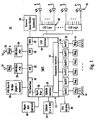
- FIG. 1 is a block diagram of a packet switched system 10 which provides the environment of the present invention.
- the packet switched network includes an integrated multiport switch (IMS) 12 that enables communication of data packets between network stations.
- the network stations may have different configurations. In the current example, twenty-four (24) 10 megabit per second (Mb/s) network stations 14 send and receive data at a network data rate of 10 Mb/s, and two 100 Mb/s network stations 16 send and receive data packets at a network speed of 100 Mb/s.
- the multiport switch 12 selectively forwards data packets received from the network stations 14 or 16 to the appropriate destination, based upon Ethernet protocol.
- the 10 Mb/s network stations 14 send and receive data packets to and from the multiport switch 12 via a media 18 and according to half-duplex Ethernet protocol.
- the Ethernet protocol ISO/IEC 8802-3 (ANSI/IEEE Std. 802.3, 1993 Ed.) defines a half-duplex media access mechanism that permits all stations 14 to access the network channel with equality. Traffic in a half-duplex environment is not distinguished or prioritized over the medium 18. Rather, each station 14 includes an Ethernet interface card that uses carrier-sense multiple access with collision detection (CSMA/CD) to listen for traffic on the media. The absence of network traffic is detected by sensing a deassertion of a receive carrier on the media.
- CSMA/CD carrier-sense multiple access with collision detection
- Any station 14 having data to send will attempt to access the channel by waiting a predetermined time after the deassertion of a receive carrier on the media, known as the interpacket gap interval (IPG). If a plurality of stations 14 have data to send on the network, each of the stations will attempt to transmit in response to the sensed deassertion of the receive carrier on the media and after the IPG interval; resulting in a collision. Hence, the transmitting station will monitor the media to determine if there has been a collision due to another station sending data at the same time. If a collision is detected, both stations stop, wait a random amount of time, and retry transmission.
- IPG interpacket gap interval
- the 100 Mb/s network stations 16 preferably operate in full-duplex mode according to the proposed Ethernet standard IEEE 802.3x Full-Duplex with Flow Control - Working Draft (0.3).
- the full-duplex environment provides a two-way, point-to-point communication link between each 100 Mb/s network station 16 and the multiport switch 12, so that the IMS and the respective stations 16 can simultaneously transmit and receive data packets without collisions.
- the 100 Mb/s network stations 16 each are coupled to network media 18 via 100 Mb/s physical (PHY) devices 26 of the type known by the registered trade marks 100 Base-TX, 100 Base-T4, or 100 Base-FX.
- the multiport switch 12 includes a media independent interface (MII) 28 that provides a connection to the physical devices 26.
- MII media independent interface
- the 100 Mb/s network stations 16 may be implemented as servers or routers for connection to other networks.
- the 100 Mb/s network stations 16 may also operate in half-duplex mode, if desired.
- the 10 Mb/s network stations 14 may be modified to operate according to full-duplex protocol with flow control.
- the packet switched system 10 includes a series of switch transceivers 20, labelled QuEST, that perform time division multiplexing and time division demultiplexing for data packets transmitted between the multiport switch 12 and the 10 Mb/s stations 14.
- a magnetic transformer module 19 maintains the signal waveform shapes on the media 18.
- the multiport switch 12 includes a transceiver interface 22 that transmits and receives data packets to and from each switch transceiver 20 using a time-division multiplexed protocol across a single serial non-return to zero (NRZ) interface line 24.
- the switch transceiver 20 receives packets from the serial NRZ interface line 24, demultiplexes the received packets, and outputs the packets to the appropriate end station 14 via the network media 18.
- each switch transceiver 20 has four independent 10 Mb/s twisted-pair ports and uses 4: 1 multiplexing across the serial NRZ interface enabling a four-fold reduction in the number of PINs required by the multiport switch 12.
- the multiport switch 12 contains a decision making engine, switching engine, buffer memory interface, configuration/control/status registers, management counters, and MAC (media access control) protocol interface to support the routing of data packets among the Ethernet ports serving the network stations 14 and 16.
- the multiport switch 12 also includes enhanced functionality to make intelligent switching decisions, and to provide statistical network information in the form of management information base (MIB) objects to an external management entity, as described below. Additional interfaces are provided to enable external storage of packet data and switching logic in order to minimize the chip size of the multiport switch 12.
- the multiport switch 12 includes a synchronous dynamic RAM (SDRAM) interface 32 that provides access to an external memory 34 for storage of received frame data, memory structures, and MIB counter information.
- SDRAM synchronous dynamic RAM
- the memory 34 may be an 80, 100 or 120 MHz synchronous DRAM having a memory size of 2 or 4 Mb.
- a management port 36 enables an external management entity to control overall operations of the multiport switch 12 by via management MAC interface 38.
- PCI interface 39 enables access by the management entity via a PCI host and bridge 40.
- the PCI host and bridge 40 may serve as an expansion bus for a plurality of IMS devices.
- An internal decision making engine within switch 12 selectively transmits data packets received from one source to at least one destination station.
- an external rules checker may be utilized.
- External rules checker interface (ERCI) 42 allows use of an external rules checker 44 to make frame forwarding decisions in substitution for the internal decision making engine. Hence, frame forwarding decisions can be made either by the internal switching engine or the external rules checker 44.
- LED interface 46 clocks out the status of conditions per port and drives LED external logic 48.
- the LED external logic 48 drives LED display elements 50 that are human readable.
- An oscillator 30 provides a 40 MHz clock input for the system functions of the multiport switch 12.
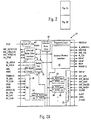
- Fig. 2 is a more detailed block diagram of a multiport switch, related to the present invention, that may be used in the packet switched system of Fig. 1.
- the multiport switch 12 includes twenty-four (24) 10 Mb/s media access control (MAC) ports 60 for sending and receiving data packets in half-duplex between the respective 10 Mb/s network stations 14 (ports 1-24), and two 100 Mb/s MAC ports 62 for sending and receiving data packets in full-duplex between the respective 100 Mb/s network stations 16 (ports 25, 26).
- the management interface 36 also operates according to MAC layer protocol (port 0).
- Each of the MAC ports 60, 62 and 36 contains conventional logic and register access control circuitry that enables control of data transmission, data reception, and collision mediation at the port.
- a receive first-in-first-out (FIFO) buffer 64 and a transmit FIFO buffer 66 are also provided at each port.
- External memory interface 32 is connected by one common bus to each of the MAC receive FIFO buffers and by another common bus to each of the MAC transmit FIFO buffers.
- Data packets from a network station are received by the corresponding MAC port and stored in the corresponding receive FIFO buffer 64.
- the received data packet is output from the corresponding receive FIFO buffer 64 to the external memory interface 32 for storage in the external memory 34.
- the header of the received packet is also forwarded to a decision making engine, comprising an internal rules checker 68 and an external rules checker interface 42, to determine which MAC ports will output the data packet. Whether the packet header is forwarded to internal rules checker 68 or external rules checker interface 42 is dependent on the operational configuration of multiport switch 12.
- Use of the external rules checker 44 provides advantages such as increased capacity, a random-based ordering in the decision queue that enables frame forwarding decisions to be made before the frame is completely buffered to external memory, and enables decisions to be made in an order independent from the order in which the frames were received by the multiport switch 12.
- the internal rules checker 68 and external rules checker 44 provide the decision making logic for determining the destination MAC port for a given data packet.
- the decision making engine may indicate that a given data packet is to be output to either a single port, multiple ports, or all ports (i.e., broadcast).
- Each data packet includes a header having source and destination address, in accordance with which the decision making engine can identify the appropriate output MAC port(s).
- the destination address may correspond to a virtual address, in which case the decision making engine identifies output ports for a plurality of network stations.
- a received data packet may include a VLAN (virtual LAN) tagged frame according to IEEE 802. 1d protocol that specifies another network (via a 100 Mb/s stations 16) or a prescribed group of stations.
- the internal rules checker 68 or the external rules checker 44 via the interface 42 will decide whether a frame temporarily stored in the buffer memory 34 should be output to a single MAC port or multiple MAC ports.
- the decision making engine outputs a forwarding decision to a switch subsystem 70 m the form of a port vector identifying each MAC port that should receive the data packet.
- the port vector from the appropriate rules checker includes the address location storing the data packet in the external memory 34, and the identification of the MAC ports to receive the data packet for transmission (e.g., MAC ports 0-26).
- the switch subsystem 70 fetches the data packet identified in the port vector from the external memory 34 via the external memory interface 32, and supplies the retrieved data packet to the appropriate transmit FIFO 66 of the identified ports.
- a management data interface 72 enables the multiport switch 11 to exchange control and status information with the switch transceivers 20 and the 100 Mb/s physical devices 26 according to the MII management specification (IEEE 802.3u).
- the management data interface 72 also outputs a management data clock (MDC) providing a timing reference on the bidirectional management data IO (MDIO) signal path.
- MDC management data clock
- the PCI interface 39 is a 32-bit PCI revision 2.1 compliant slave interface for access by the PCI host processor 40 to internal IMS status and configuration registers 74, and access external memory SDRAM 34.
- the PCI interface 39 can also serve as an expansion bus for multiple IMS devices.
- the management port 36 interfaces to an external MAC engine through a standard seven-wire inverted serial GPSI interface, enabling a host controller access to the multiport switch 12 via a standard MAC layer protocol.
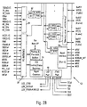
- Fig. 3 is a block diagram illustrating media access control for the system of Fig. 1 in accordance with the present invention.
- a single media access control logic unit 80 is provided to be used in common for the twenty-four (24) 10 Mb/s switch ports 60 and the MII management control port.
- Unit 80 is coupled to transceiver interface 22 by means of a transmit connection and a receive connection.
- the unit 80 is also connected to the transmit FIFO 66 and the receive FIFO 64 at each port 60.
- FIFO 64 and FIFO 66 are connected to bus 84. While shown as a single line, bus 84 represents a common receive bus connection among all port 60 receive FIFOs and the external memory interface 32, as well as a common transmit bus connection among all port 60 transmit FIFOs and external memory interface 32.
- a state memory control unit 82 stores the media access state of each of ports 60.
- Unit 82 is connected to unit media access control logic unit 80 for transfer of state data therebetween.
- a data communication also exists between the state memory control unit 82 and transceiver interface 22.
- State memory control unit 82 has a clock input for receiving an 80 Mhz signal. As to be more fully described below, this clock signal provides synchronization timing for time shared media access control functionality performed by logic unit 80 for each of the twenty four switch ports 60.
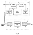
- Fig. 4 is a more detailed block diagram of a preferred configuration of the media access control logic unit 80 and the state memory control unit 82 of Fig. 3.
- State memory control unit 82 comprises state memory 90, output register 92, input register 94, counter 96 and delay circuit 98.
- State memory 90 which stores the access states at each of the ports 60, may be embodied, for example, by a random access memory (RAM) or by one or more registers dedicated to each port 60.
- Output register 92 and input register 94 are connected to state memory 90 respectively to receive data from or input data to the state memory.
- Counter 96 which has an input from the 80 Mhz clock source, outputs a data signal having sufficient bits to uniquely identify each of the ports 60.
- the counter output signal preferably is five bits in length. This signal is incremented in value with each received clock signal pulse.
- the counter output signal is applied to output register 92, thereby to identify the port for which the state memory data is to be accessed from state memory 90.
- the counter output signal is also applied to delay circuit 98, which holds and delays the signal for a plurality of clock stages.
- the output of the delay circuit 98 is applied to the input register 94, thereby identifying that port for which data is to be stored in the state memory 90.
- the time period between retrieval of stored data for a given port and writing of new data for that port is dependent upon the number of clock stages delayed by the delay circuit 98. Determination of this number is coordinated with the number of clock pipeline stages required by the media access control logic unit 80.
- the registers, counter and delay circuits are each conventional, well-known elements.
- Registers 102 are connected to input data to the logic unit, as acquired from the state output register 92 and the transceiver interface 22. After processing the data received from registers 102, the logic unit outputs the processed data to registers 104.
- This processed data includes instructions to be transmitted to the FIFOs at the associated port, any communication data to be transferred, and the change, if any, of the port access state, the latter being transmitted to the state input register 94.
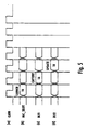
- Fig. 5 is waveform diagram depicting the staged pipeline operation.
- the delay circuit 98 contains two delay stages.
- Waveform (a) represents the 80 Mhz clock signal.
- Waveform (b) represents the output of counter 96 during each cycle of the clock signal of waveform (a). This signal identifies a MAC port and is incremented with each clock signal, thereby to establish sequential time shared operation.
- Each clock cycle thus defines a "MAC slot" corresponding to a port identified by the counter.
- the MAC slot identified by the counter output during the first clock cycle is slot 16.
- Waveforms (c) and (d) represent MAC slot identification for two stages of delay during each clock signal cycle.
- MAC slot 16 is indicated by waveform (c) during the second clock cycle and by waveform (d) during the third clock cycle.
- Each of waveforms (b) through (c) is associated with one of three stages of media access control activity (indicated in the figure by the broad labels "launch.” “capture” and “update”) and thus identifies the MAC port to which that activity relates.
- the three activities operate concurrently during each clock cycle respectively for different MAC ports.
- the figure illustrates the three stages of operation for MAC port 16.
- the launch stage for this port occurs during the first illustrated clock cycle.
- the counter identifies port 16 for which data is accessed from the state memory 90 and held in register 92.
- the capture stage for MAC port 16 takes place.
- Data from the register 92 and the transceiver interface are then input to the registers 80 and processed by the combinational logic unit 100, the resulting data held in registers 104. Also during this cycle, the counter will have identified the next MAC port for launch stage operation. During the next clock cycle, the update stage for MAC port 16 takes place. State update data from registers 104 are transferred to input register 94 and stored in state memory 90. Operational data are transferred to the appropriate FIFO. Media access control continues in this manner sequentially for each MAC port.
- the present invention thus advantageously provides efficient media access control while conserving chip architecture. Only the preferred embodiment of the invention and but a few examples of its versatility are shown and described in the present disclosure. It is to be understood that the invention is capable of use in various other combinations and environments and is capable of changes or modifications within the scope of the inventive concept as expressed herein.
Claims (13)
- Integrierter Multiport-Netzschalter (12) zum Anschließen an ein Datennetz zwecks Ermöglichung einer Datenübertragung zwischen mehreren mit dem Datennetz gekoppelten Fernstationen, wobei der Schalter einen Logik-Chip aufweist, der folgendes umfasst:dadurch gekennzeichnet, dassmehrere Ports (60,62) zum Übermitteln von Datenblöcken zu und Empfangen von Datenblöcken von dem Datennetz; undeine zentral auf dem Chip angeordnete Medienzugriffssteuer- (MAC-) Schaltungsanordnung (80) zum Steuern des Datenblockflusses an jedem Port, wobei die MAC-Schaltungsanordnung auf Zeitteilbasis jeweils mit jedem Port gekoppelt ist;
die MAC-Schaltungsanordnung (80) eine Logik-Schaltungseinrichtung (100,102,104) zum Durchführen von Medienzugriffs-Steuerfunktionen und eine Zustandsspeichereinrichtung (82) zum Speichern von Medienzugriffszuständen der mehreren Ports (60) aufweist. - Integrierter Multiport-Netzschalter nach Anspruch 1, bei dem die Medienzugriffs-Steuerfunktionen Datenübermittlung, Datenempfang und Vermittlung bei Datenkollisionen umfassen.
- Integrierter Multiport-Netzschalter nach Anspruch 1 oder 2, ferner mit mindestens einem Eingangsempfangs-FIFO-Puffer (64) an jedem Port zum temporären Halten von aus dem Netz empfangenen Datenblöcken an dem jeweiligen Port und mindestens einem Übermittlungs-FIFO-Puffer (66) an jedem Port zum temporären Halten von an das Netz zu übermittelnden Datenblöcken an dem jeweiligen Port, wobei der FIFO-Puffer (64,66) mit der Logik-Schaltungseinrichtung (100,102,104) gekoppelt ist.
- Integrierter Multiport-Netzschalter nach Anspruch 3, bei dem der Schalter (12) mehrere jeweiligen Netz-Fernstationen (14) zugeordnete Schalter-Sendeempfänger (20) aufweist und der Chip ferner umfasst:ein zwischen der Logik-Schaltungseinrichtung (100,102,104) und den mehreren Schalter-Sendeempfängern (20) gekoppeltes Zeitmultiplex-/- demultiplex-Sendeempfänger-Interface (22).
- Integrierter Multiport-Netzschalter nach Anspruch 4, bei dem mindestens einer der Schalter-Sendeempfänger (20) eine Multiplex-/Demultiplexeinrichtung für die Zeitteilung von Datenübertragungen für mehrere Fernstationen (14) aufweist.
- Integrierter Multiport-Netzschalter nach Anspruch 5, bei dem die Zustandsspeichereinrichtung (82) aufweist:einen Datenspeicher (90) mit Teilbereichen, die jeweils Daten zugewiesen sind, die den aktuellen Zustand jedes Ports repräsentieren;ein mit dem Datenspeicher (90) gekoppeltes Ausgangsregister (92) zum Empfangen gespeicherter Daten aus dem Datenspeicher, die den Zustand eines ersten bestimmten der Ports (60) repräsentieren, wobei das Ausgangsregister (92) zum Ausgeben von Daten an die Logik-Schaltungseinrichtung (100,102,104) mit dieser gekoppelt ist;ein mit der Logik-Schaltungseinrichtung (100,102,104) gekoppeltes Eingangsregister (94) zum Empfangen von Daten von der Logik-Schaltungseinrichtung, die den Zustand eines zweiten bestimmten der Ports (60) repräsentieren, wobei das Eingangsregister zum Eingeben von Daten in den Datenspeicher (90) mit diesem gekoppelt ist; undeine Zugriffseinrichtung (96,98) zum Zugreifen auf die Datenspeicher-Teilbereiche in sequentiellen getakteten Stufen.
- Integrierter Multiport-Netzschalter nach Anspruch 6, bei dem die Datenspeicher-Teilbereiche durch Schalterportadressen identifiziert werden und die Zugriffseinrichtung aufweist:wobei aktualisierte Medienzugriffs-Zustandsdaten für die von dem Zähler gelieferte Portadresse von der Logik-Schaltungseinrichtung (100, 102,104) empfangen und an den entsprechenden Datenspeicher-Teilbereich angelegt werden.einen Zähler (96), der auf ein Taktsignal anspricht und zum sequentiellen Zuführen einer Portadresse, für die Daten aus dem entsprechenden Datenspeicher-Teilbereich zurückgewonnen werden, zu dem Ausgangsregister (92) mit diesem gekoppelt ist; undeine zwischen dem Zähler (96) und dem Eingangsregister (94) geschaltete Verzögerungseinrichtung (98) zum Verzögern des Anlegens der von dem Zähler (96) gelieferten Portadresse an das Eingangsregister um mindestens eine Taktstufe;
- Integrierter Multiport-Netzschalter nach Anspruch 7, bei dem die Logik-Schaltungseinrichtung (100,102,104) Register (102) mit einem ersten Eingang zum Empfangen von Daten aus dem Ausgangsregister (92) und einem zweiten Eingang zum Empfangen von Daten von dem Sendeempfänger-Interface aufweist.
- Verfahren zum Steuern eines Medienzugriffs an mehreren Ports eines integrierten Multiport-Netzschalters (12) mit einem Logik-Chip, der mit einem Datennetz gekoppelt ist, um eine Datenübertragung zwischen mehreren mit dem Datennetz verbundenen Fernstationen (14) zu ermöglichen,
gekennzeichnet durch folgende Schritte:wobei der Ausführschritt umfasst:sequentielles Auslesen des Zugriffszustands jedes der mehreren Ports (60,62) aus einer Zustandsspeichereinrichtung (82), die zentral auf dem Logik-Chip angeordnet ist und gemeinsam für sämtliche Ports vorgesehen ist;im Anschluss an jeden sequentiellen Ausleseschritt, Ausführen einer Datenübertragungs-Zugriffsfunktion an dem entsprechenden Port in Reaktion auf von einem mit dem Port gekoppelten Sendeempfänger-Interface (22) empfangene Daten; undim Anschluss an jeden Ausführschritt, Aktualisieren der gemeinsamen Zustandsspeichereinrichtung (82);Verarbeiten von in dem Ausleseschritt ausgelesenen Daten und von dem Interface (22) empfangenen Daten in einer Logik-Schaltungseinrichtung (100,102,104), die zentral auf dem Logik-Chip angeordnet ist und gemeinsam für sämtliche Ports vorgesehen ist; undErzeugen neuer Zustandsdaten für den Port in der gemeinsamen Logik-Schaltungseinrichtung (100,102,104). - Verfahren nach Anspruch 9, bei dem der Schritt des sequentiellen Auslesens das Adressieren der Zustandsspeichereinrichtung (82) in Reaktion auf das Ausgangssignal eines getakteten Zählers umfasst und der Aktualisierungsschritt umfasst:Verzögern des Ausgangssignals des getakteten Zählers;Adressieren der Zustandsspeichereinrichtung (82) in Reaktion auf das verzögerte Ausgangssignal des getakteten Zählers; undSchreiben neuer Zustandsdaten in die Zustandsspeichereinrichtung (82) an der in dem Adressierschritt verwendeten Adresse.
- Verfahren nach Anspruch 9 oder 10, bei dem der Ausführschritt das Übermitteln von in einem Übermittlungspuffer (66) gespeicherten Daten an dem Port zu dem Datennetz umfasst.
- Verfahren nach Anspruch 9, 10 oder 11, bei dem der Ausführschritt das Empfangen von Daten aus dem Netz an einem Empfangspuffer (64) an dem Port umfasst.
- Verfahren nach Anspruch 9, 10, 11 oder 12, bei dem der Ausführschritt das Vermitteln bei einer Datenkollision an dem Port umfasst.
Applications Claiming Priority (5)
| Application Number | Priority Date | Filing Date | Title |
|---|---|---|---|
| US3802597P | 1997-02-14 | 1997-02-14 | |
| US38025P | 1997-02-14 | ||
| US992921 | 1997-12-18 | ||
| US08/992,921 US6094436A (en) | 1997-02-14 | 1997-12-18 | Integrated multiport switch having shared media access control circuitry |
| PCT/US1998/001760 WO1998036535A1 (en) | 1997-02-14 | 1998-01-29 | Integrated multiport switch having shared media access control circuitry |
Publications (2)
| Publication Number | Publication Date |
|---|---|
| EP0976226A1 EP0976226A1 (de) | 2000-02-02 |
| EP0976226B1 true EP0976226B1 (de) | 2004-03-17 |
Family
ID=26714749
Family Applications (1)
| Application Number | Title | Priority Date | Filing Date |
|---|---|---|---|
| EP98903831A Expired - Lifetime EP0976226B1 (de) | 1997-02-14 | 1998-01-29 | Integrierte multiport-vermittlung mit geteilter mediumzugriffssteuerungsschaltung |
Country Status (5)
| Country | Link |
|---|---|
| US (1) | US6094436A (de) |
| EP (1) | EP0976226B1 (de) |
| JP (1) | JP4072583B2 (de) |
| DE (1) | DE69822456T2 (de) |
| WO (1) | WO1998036535A1 (de) |
Families Citing this family (20)
| Publication number | Priority date | Publication date | Assignee | Title |
|---|---|---|---|---|
| US6272552B1 (en) * | 1998-09-24 | 2001-08-07 | Hewlett-Packard Company | Dual channel 100Base-T link for computer networks |
| US6317804B1 (en) * | 1998-11-30 | 2001-11-13 | Philips Semiconductors Inc. | Concurrent serial interconnect for integrating functional blocks in an integrated circuit device |
| US6975637B1 (en) * | 1999-01-27 | 2005-12-13 | Broadcom Corporation | Apparatus for ethernet PHY/MAC communication |
| US6934261B1 (en) | 2000-11-17 | 2005-08-23 | Advanced Micro Devices, Inc. | Method to select dynamically between MACs of network device depending on network topology |
| US6781989B1 (en) | 2000-11-17 | 2004-08-24 | Advanced Micro Devices, Inc. | Method to support VLANs on a phoneline network |
| US6947438B1 (en) | 2000-11-17 | 2005-09-20 | Advanced Micro Devices, Inc. | PCI and MII compatible home phoneline networking alliance (HPNA) interface device |
| US6853645B1 (en) | 2000-11-17 | 2005-02-08 | Advanced Micro Devices, Inc. | PCI and MII compatible home phoneline networking alliance (HPNA) interface device |
| US6894999B1 (en) | 2000-11-17 | 2005-05-17 | Advanced Micro Devices, Inc. | Combining VLAN tagging with other network protocols allows a user to transfer data on a network with enhanced security |
| US6912199B1 (en) | 2000-12-28 | 2005-06-28 | Advanced Micro Devices, Inc. | Method to select transmission rate for network device |
| JP4041656B2 (ja) * | 2001-03-02 | 2008-01-30 | 株式会社日立製作所 | ストレージシステム及びストレージシステムにおけるデータ送受信方法 |
| US8018851B1 (en) | 2004-06-30 | 2011-09-13 | Marvell Israel (Misl) Ltd. | Flow control for multiport PHY |
| US7599686B2 (en) * | 2005-05-06 | 2009-10-06 | Dell Products L.P. | Systems and methods for RF spectrum management |
| US7551641B2 (en) | 2005-07-26 | 2009-06-23 | Dell Products L.P. | Systems and methods for distribution of wireless network access |
| US7716403B2 (en) * | 2005-09-30 | 2010-05-11 | Rockwell Automation Technologies, Inc. | Information technology integration with automation systems |
| US20080114899A1 (en) * | 2006-10-05 | 2008-05-15 | Holt John M | Switch protocol for network communications |
| WO2013134810A1 (en) | 2012-03-12 | 2013-09-19 | Zeptoip Pty Ltd | A network device and a method for networking |
| EP2723118B1 (de) | 2012-09-28 | 2019-03-27 | Juniper Networks, Inc. | Verfahren und Vorrichtung zur Steuerung von drahtlosen Zugangspunkten |
| US9674030B2 (en) * | 2012-09-28 | 2017-06-06 | Juniper Networks, Inc. | Methods and apparatus for a common control protocol for wired and wireless nodes |
| US10452574B2 (en) * | 2018-07-26 | 2019-10-22 | Intel Corporation | Read performance on a SATA storage device behind a host bus adapter |
| CN112524652B (zh) * | 2020-11-30 | 2022-12-27 | 云米互联科技(广东)有限公司 | 一种集成灶的控制方法 |
Family Cites Families (9)
| Publication number | Priority date | Publication date | Assignee | Title |
|---|---|---|---|---|
| US5177739A (en) * | 1990-04-20 | 1993-01-05 | Racal Data Communications, Inc. | Multiport - multipoint digital data service |
| WO1991018462A1 (en) * | 1990-05-18 | 1991-11-28 | The University Of Toronto Innovations Foundation | High bandwidth fault tolerant lan |
| EP0603444A1 (de) * | 1992-12-22 | 1994-06-29 | International Business Machines Corporation | Sternförmiger Schalter mit Tokenzugriff |
| EP0603443A1 (de) * | 1992-12-22 | 1994-06-29 | International Business Machines Corporation | Tokensternbrücke |
| US5515376A (en) * | 1993-07-19 | 1996-05-07 | Alantec, Inc. | Communication apparatus and methods |
| US5864554A (en) * | 1993-10-20 | 1999-01-26 | Lsi Logic Corporation | Multi-port network adapter |
| US5432775A (en) * | 1993-12-03 | 1995-07-11 | Advanced Micro Devices, Inc. | Auto negotiation system for a communications network |
| US5467351A (en) * | 1994-04-22 | 1995-11-14 | At&T Corp. | Extendible round robin local area hub network |
| US5790786A (en) * | 1995-06-28 | 1998-08-04 | National Semiconductor Corporation | Multi-media-access-controller circuit for a network hub |
-
1997
- 1997-12-18 US US08/992,921 patent/US6094436A/en not_active Expired - Lifetime
-
1998
- 1998-01-29 EP EP98903831A patent/EP0976226B1/de not_active Expired - Lifetime
- 1998-01-29 JP JP53577398A patent/JP4072583B2/ja not_active Expired - Fee Related
- 1998-01-29 WO PCT/US1998/001760 patent/WO1998036535A1/en active IP Right Grant
- 1998-01-29 DE DE69822456T patent/DE69822456T2/de not_active Expired - Lifetime
Also Published As
| Publication number | Publication date |
|---|---|
| WO1998036535A1 (en) | 1998-08-20 |
| EP0976226A1 (de) | 2000-02-02 |
| JP2001511977A (ja) | 2001-08-14 |
| JP4072583B2 (ja) | 2008-04-09 |
| DE69822456D1 (de) | 2004-04-22 |
| US6094436A (en) | 2000-07-25 |
| DE69822456T2 (de) | 2004-12-23 |
Similar Documents
| Publication | Publication Date | Title |
|---|---|---|
| US6151322A (en) | Multiport data switch having data frame VLAN tagging and VLAN stripping | |
| EP0976226B1 (de) | Integrierte multiport-vermittlung mit geteilter mediumzugriffssteuerungsschaltung | |
| US6130891A (en) | Integrated multiport switch having management information base (MIB) interface temporary storage | |
| US6373848B1 (en) | Architecture for a multi-port adapter with a single media access control (MAC) | |
| US7027437B1 (en) | Network switch multiple-port sniffing | |
| US6463032B1 (en) | Network switching system having overflow bypass in internal rules checker | |
| US6091707A (en) | Methods and apparatus for preventing under-flow conditions in a multiple-port switching device | |
| US6466580B1 (en) | Method and apparatus for processing high and low priority frame data transmitted in a data communication system | |
| EP0960504B1 (de) | Mehrfachkopiewarteschlangestruktur mit einem suchbaren cachespeicherbereich | |
| EP0960512A1 (de) | Gerät und verfahren zur erzeugung von verwaltungspaketen zur übertragung zwischen einer netzwerkvermittlungsstelle und einer host steuereinheit | |
| US6084878A (en) | External rules checker interface | |
| US6724769B1 (en) | Apparatus and method for simultaneously accessing multiple network switch buffers for storage of data units of data frames | |
| US6393028B1 (en) | Method and apparatus for providing EOF for frame modification | |
| US6895015B1 (en) | Dynamic time slot allocation in internal rules checker scheduler | |
| US6741589B1 (en) | Apparatus and method for storing data segments in a multiple network switch system using a memory pool | |
| US6597693B1 (en) | Common scalable queuing and dequeuing architecture and method relative to network switch data rate | |
| EP1266492A1 (de) | Vorrichtung und verfahren zur speicherteilung in einer konfiguration mit einzelring-datenbusverbindung | |
| US20060023716A1 (en) | Bit bucket | |
| US6891843B1 (en) | Apparatus and method for sharing memory using extra data path having multiple rings | |
| TW415151B (en) | Integrated multiport switch having shared media access control circuitry |
Legal Events
| Date | Code | Title | Description |
|---|---|---|---|
| PUAI | Public reference made under article 153(3) epc to a published international application that has entered the european phase |
Free format text: ORIGINAL CODE: 0009012 |
|
| 17P | Request for examination filed |
Effective date: 19990827 |
|
| AK | Designated contracting states |
Kind code of ref document: A1 Designated state(s): DE GB |
|
| GRAP | Despatch of communication of intention to grant a patent |
Free format text: ORIGINAL CODE: EPIDOSNIGR1 |
|
| GRAS | Grant fee paid |
Free format text: ORIGINAL CODE: EPIDOSNIGR3 |
|
| GRAA | (expected) grant |
Free format text: ORIGINAL CODE: 0009210 |
|
| AK | Designated contracting states |
Kind code of ref document: B1 Designated state(s): DE GB |
|
| REG | Reference to a national code |
Ref country code: GB Ref legal event code: FG4D |
|
| REF | Corresponds to: |
Ref document number: 69822456 Country of ref document: DE Date of ref document: 20040422 Kind code of ref document: P |
|
| PLBE | No opposition filed within time limit |
Free format text: ORIGINAL CODE: 0009261 |
|
| STAA | Information on the status of an ep patent application or granted ep patent |
Free format text: STATUS: NO OPPOSITION FILED WITHIN TIME LIMIT |
|
| 26N | No opposition filed |
Effective date: 20041220 |
|
| REG | Reference to a national code |
Ref country code: GB Ref legal event code: 732E Free format text: REGISTERED BETWEEN 20091210 AND 20091216 |
|
| PGFP | Annual fee paid to national office [announced via postgrant information from national office to epo] |
Ref country code: GB Payment date: 20101215 Year of fee payment: 14 |
|
| PGFP | Annual fee paid to national office [announced via postgrant information from national office to epo] |
Ref country code: DE Payment date: 20110131 Year of fee payment: 14 |
|
| GBPC | Gb: european patent ceased through non-payment of renewal fee |
Effective date: 20120129 |
|
| PG25 | Lapsed in a contracting state [announced via postgrant information from national office to epo] |
Ref country code: GB Free format text: LAPSE BECAUSE OF NON-PAYMENT OF DUE FEES Effective date: 20120129 Ref country code: DE Free format text: LAPSE BECAUSE OF NON-PAYMENT OF DUE FEES Effective date: 20120801 |
|
| REG | Reference to a national code |
Ref country code: DE Ref legal event code: R119 Ref document number: 69822456 Country of ref document: DE Effective date: 20120801 |