EP0968568B1 - Comportement d'une boucle asservie en phase a bande etroite a effet d'emulation sur une boucle asservie en phase a bande large - Google Patents
Comportement d'une boucle asservie en phase a bande etroite a effet d'emulation sur une boucle asservie en phase a bande large Download PDFInfo
- Publication number
- EP0968568B1 EP0968568B1 EP98911466A EP98911466A EP0968568B1 EP 0968568 B1 EP0968568 B1 EP 0968568B1 EP 98911466 A EP98911466 A EP 98911466A EP 98911466 A EP98911466 A EP 98911466A EP 0968568 B1 EP0968568 B1 EP 0968568B1
- Authority
- EP
- European Patent Office
- Prior art keywords
- frequency
- phase
- signal
- error signal
- locked loop
- Prior art date
- Legal status (The legal status is an assumption and is not a legal conclusion. Google has not performed a legal analysis and makes no representation as to the accuracy of the status listed.)
- Expired - Lifetime
Links
Images


Definitions
- the present invention relates generally to phase-locked loop circuits, and more particularly to a phase-locked loop circuit which exhibits a tightly controlled capture range for locking an output signal to a data signal, while also providing a wide frequency capture range for initially pulling the output signal within a wider, predetermined frequency range.
- EP 0 402 113 discloses a VCO frequency control circuit.
- a phase error generator generates a digital phase error signal from an input signal.
- the phase error signal is converted to a digital frequency error signal by a digital integrator.
- the error signals are added and the result is supplied to a DAC in the phase-locked loop for providing an analog output indicative of PLL frequency error. Outputs from two DACs are summed and the resultant current is used to adjust the VCO frequency.
- WO 96 17435 discloses a steered frequency phase-locked loop.
- the loop comprises phase and frequency detectors, receiving an output from a VCO.
- the outputs from the detectors are individually gained and filtered, and fed to a summer.
- the frequency of the signal produced by a VCO deviates from a free-running frequency depending on the input from the summer.
- US 5,546,433 discloses a digital phase-locked loop having frequency offset cancellation circuitry.
- a phase comparator generates phase error signal samples from a digital data signal.
- a phase/frequency detector 50 generates either UP or DOWN output pulses depending on whether an output from a frequency synthesizer leads or lags a clock signal from a VCO.
- a phase error clock signal is generated by a logic circuit, and fed to a counter which integrates the phase error in the signal.
- the secondary frequency offset value is converted to an analog signal and combined with signals from the phase comparator to generate an analog oscillator control signal.
- U.S. 5,525,935 discloses a high-speed bit synchronizer with multi-stage control structure. An output signal from a phase comparator is fed to a phase difference output controller. The output from a frequency comparator is fed to a frequency synchronous signal detector. The phase difference output controller receives either a synchronous or an asynchronous signal from the frequency synchronous signal detector, whereupon the phase difference output controller transfers, or does not transfer, respectively, its output to an integrator.
- Fig. 1 illustrates a prior art phase-locked loop (PLL) 10 feedback circuit.
- the PLL 10 is a feedback circuit that is often used to reduce an error term toward zero.
- the error term is the phase difference between an input signal and a reference signal.
- the basic component building blocks of a PLL are a phase comparator 12 and a voltage-controlled oscillator (VCO) 14.
- the PLL incorporates the VCO 14 in the feedback loop.
- a VCO is an oscillator whose output frequency is a function of its input voltage.
- the phase comparator 12 compares the phase of the input signal on line 16 to the phase of the signal at the output of the VCO on line 18.
- the output frequency of the VCO 14 is adjusted in a manner which forces this difference down to zero.
- the output signal on line 20 is fed back to the VCO 14 to provide a signal proportional to the phase difference between the signals on lines 16 and 18.
- phase-locked loops are also widely used in communication systems for coherent carrier tracking, and threshold extension, bit synchronization and symbol synchronization.
- the PLLs as used in the data communications system of the present invention are used to lock to a receive signal and to subsequently provide the receive clock for that signal.
- the PLL lock information generated from a data signal is poor, and is therefore not capable of pulling the PLL very far in frequency. Often the frequency range of the PLL is wider than this narrow "capture" range.
- the oscillation frequency of the PLL must somehow be brought close enough to the data signal frequency for the PLL to lock to the data signal. This can be done, as shown in Fig. 1, by first locking the PLL 10 to the frequency of a reference signal on line 22, which is close in frequency to the data signal on line 24. When the PLL 10 is locked to the reference signal on line 22, the input of the PLL 10 is switched over to the data signal on line 24. Although this procedure works, it requires control circuitry 26 to switch from the reference signal on line 22 to the data signal on line 24, and then back again if phase lock is lost.
- phase-locked loop which has a wide frequency capture range for pulling the PLL within a predetermined frequency range, yet has a well-controlled and narrow frequency capture range for locking to the actual data signal, without the use of switching control circuitry such as control circuitry 26.
- the present invention discloses a phase-locked loop that exhibits a tightly controlled capture range for locking an output signal to a data signal, while also providing a wide frequency capture range for initially pulling the output signal within a wider, predetermined frequency range as defined in the appended claims.
- the apparatus detects a frequency difference between at least one reference signal and a phase-locked loop (PLL) output signal, and generates a frequency error signal in response to the frequency difference.
- a phase difference is detected between a received input signal and the PLL output signal, and a phase error signal is generated in response to this phase difference.
- the frequency error signal and the phase error signal are combined, and this combined signal controls the frequency of the output signal.
- the frequency error signal dominates the concurrently generated phase error signal when the frequency difference is outside of a predetermined frequency range. This dominating signal overdrives the phase error signal by increasing the amplitude of the frequency error signal.
- a multiple-stage phase-locked loop has an inherently wide actual signal capture range and a narrow effective signal capture range.
- the PLL includes a first detection mechanism for detecting first phase differences between reference signals and an output signal, and for generating a first phase error signal when the first phase differences fall outside of a predetermined frequency range.
- the PLL further includes a second detection mechanism for detecting second phase differences between a received input signal and the output signal, and for generating a second phase error signal in response thereto.
- a signal summing mechanism combines the first phase error signal and the second phase error signal, and allows the first phase error signal to overdrive the second phase error signal when both the first and second phase error signals are active.
- the PLL also includes a voltage-controlled oscillator to control the frequency of the output signal in response to the first and second phase error signals.
- a method for phase-locking an output signal to a data signal.
- a frequency error signal is generated where a first frequency difference, measured by the frequency difference between a reference signal and the output signal, is outside of a predetermined frequency range.
- a phase error signal is generated for a second frequency difference measured by the frequency difference between the data signal and the output signal. Where the first frequency difference is outside of the predetermined frequency range, the frequency error signal overdrives the phase error signal.
- the frequency of the output signal is controlled with the phase error signal and the frequency error signal.
- the present invention provides a phase-locked loop circuit which exhibits a tightly controlled capture range for locking to a data signal, while also providing a wide frequency capture range for pulling the PLL within a wider frequency range.
- Fig. 2 is a general block diagram of one embodiment of the invention.
- the PLL 100 of Fig. 2 includes a frequency comparator 102 and a phase error detector 104 at the inputs of the PLL 100.
- the frequency comparator 102 compares the frequency of one or more reference signals to the frequency of a signal to be controlled.
- the signal to be controlled in Fig. 2 is the output signal, labeled F(CK) on line 106.
- the F(CK) signal is fed back to the frequency comparator 102 via line 108 to be compared to one or more reference signals.
- two reference signals are provided, labeled F(CENT) on line 110 and F(REF) on line 112.
- PLL 100 compares the frequency of the F(CK) signal on feedback line 108 to a combination of the reference signals on lines 110 and 112. The reference signal combination will be described in more detail in the ensuing description.
- the purpose of the frequency comparator 102 is to provide a mechanism for pulling the output of the PLL 100 within a first frequency range from which the phase error detector 104 can then tightly lock to the input signal on line 114.
- the frequency comparator 102 outputs a frequency error on line 116 that is proportional to the frequency difference between the combination of the reference signals on lines 110, 112, and the F(CK) signal on feedback line 108. Where the frequency of the F(CK) signal on feedback line 108 is greater than a combination of the reference signals F(CENT) and F(REF), a negative frequency error signal will be generated on line 116 to ultimately cause the VCO 118 to decrease the frequency of the F(CK) signal.
- the frequency comparator 102 and the phase error detector 104 operate concurrently, however the frequency comparator 102 overrides the phase error detector 104 while the frequency error on line 116 is active.
- the frequency error is active when the frequency difference, between the F(CK) signal on feedback line 108 and the combination of the reference signals F(CENT) and F(REF) on lines 110 and 112 respectively, is outside of a predetermined frequency range.
- This predetermined frequency range is bounded by a cutoff frequency, F(cutoff), above or below the combined reference signal frequency.
- F(cutoff) a cutoff frequency
- the phase error on line 120 is recognized by the VCO 118, which then adjusts the output signal F(CK) on line 106 according to the frequency difference between the F(CK) signal on feedback line 108 and the input signal on line 114.
- the frequency comparator 102 first pulls the PLL 100 output signal F(CK) on line 106 to a frequency range defined by the reference signals F(CENT) and F(REF) on lines 110 and 112 respectively. Then, when the F(CK) signal is within the predetermined frequency range, the phase error detector locks the PLL 100 output signal F(CK) to the input signal on line 114.
- the frequency comparator 102 overrides the phase error detector 104 when the frequency comparator 102 is generating a frequency error signal on line 116.
- the amplitude of the frequency comparator 102 output on line 116 is selected to be large enough to overdrive the phase error signal on line 120. Therefore, when the frequency difference between the F(CK) signal and the combination of the reference signals F(CENT) and F(REF) is outside of the predetermined frequency range, the frequency comparator 102 provides an amplified error signal which is recognized at the input of the VCO 118.
- the amplified frequency error signal on line 116 is reduced to a near zero value, and the phase error detector 104 then provides the error signal to the input of the VCO 118.
- both the frequency error signal and the phase error signal, on lines 116 and 120 respectively can be concurrently generated, while allowing only one of the signals to be significantly recognized.
- the frequency error signal the phase error signal on lines 116 and 120 are added together at the summing device 122. This allows both the frequency error signal and the phase error signal to be generated concurrently, while providing a single input signal to the VCO 118.
- the PLL 200 includes a circuit 202 for changing the order of the phase-locked loop.
- the PLL 200 is similar to PLL 100 of Fig. 2, as it includes the frequency comparator 102, the phase error detector 104, the summing circuit 122 and the VCO 118. However, these components can be applied to any order PLL.
- PLL 200 is a second order phase-locked loop, as the circuit 202 includes an integrator 204 and a summing circuit 206. As will be appreciated by those skilled in the art, the inclusion of circuit 202 results in a transfer function having two poles, thereby providing a second-order PLL.
- the resulting signal is inputted into the VCO 118 to control the frequency of the output signal F(CK) on line 106.
- the output signal F(CK) is also fed back into both the frequency comparator 102 and the phase error detector 104. This feedback provides the control signal necessary for the frequency comparator 102 and the phased error detector 104 to lock in on the frequency of the input signal on line 114.
- Any order PLL can be constructed using the teachings as herein disclosed without departing from the scope and spirit of the invention.
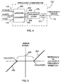
- Fig. 4 is a general block diagram of one embodiment of the frequency comparator 102.
- the preferred frequency comparator 102 is an up/down counter 300 with input signals F(CENT), F(REF) and F(CK) on lines 110, 112 and 114.
- One possible implementation is a 16-bit counter having four outputs on lines 302, 304, 306 and 308.
- the counter executes one count towards its center (i.e., it decrements the count if the count is greater than eight, and increments the count if the count is less than eight).
- the counter increments, and on the positive edge of an F(CK) pulse the counter decrements.
- the frequency comparator 102 When the count is greater than 12, the frequency comparator 102 outputs a positive error signal proportional to the amount by which the count is greater than or equal to twelve (hexadecimal C). When the count is less than 4, the frequency comparator 102 outputs a negative error signal proportional to the amount by which the count is less than four.
- the boundary logic 310 receives the count value on lines 302 through 308, and determines whether the count is less than four, between four and eleven, or greater than or equal to twelve. If the count is between four and eleven, the boundary logic 310 outputs a binary null value to ultimately generate a near zero frequency error signal on line 116. If the count is less than four, or greater than eleven, the boundary logic passes the value to a digital-to-analog (D/A) converter 312 that generates a proportional frequency error signal on line 116.
- D/A digital-to-analog
- the up/down counter 300 counts down and therefore produces a negative frequency error signal when F(CK)-F(REF) > F(CENT), which would indicate that the F(CK) signal is oscillating at a faster rate than the F(REF) and F(CENT) reference signal combination.
- the up/down counter 300 counts up and therefore produces a positive frequency error signal when F(CK)-F(REF) ⁇ F(CENT), which would indicate that the F(CK) signal is oscillating at a slower rate than the F(REF) and F(CENT) reference signal combination.
- the up/down counter 300 counts toward the center and therefore produces zero output when
- the frequency comparator 102 output i.e., the frequency error signal on line 116
- a negative frequency error signal labeled -ERR
- the -ERR signal is proportional to the amount by which the count is less than four.
- the +ERR signal is proportional to the amount by which the count is greater than or equal to twelve. Where the count is between four and eleven, the frequency error signal, shown as ERR, is approximately equal to zero.
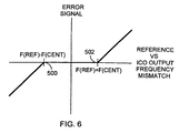
- Fig. 5 is a diagram of the transfer function of the frequency comparator 102 of Fig. 4.
- Fig. 5 illustrates the frequency error signal on line 116 as plotted against the frequency mismatch of the reference signals and the VCO 118 output.
- no error signal is generated by the frequency comparator 102 within the predetermined frequency range 400. It is within this frequency range 400 that the frequency error on line 116 does not dominate the phase error signal on line 120, and the phase error signal allows the input signal on line 114 to be locked as the F(CK) signal on line 106.
- the lower range of the frequency mismatch is shown in Fig.
- the up/down counter 300 will decrement the count when the F(CK) signal is greater than the sum of the reference signals as shown in Equation 1 below.
- F (CK) > F (REF) + F (CENT) When the F(CK) signal is greater than the sum of the reference signals, the operating point moves to the left on the transfer function of Fig. 5 until a negative error signal occurs, which is proportional to the magnitude of the frequency mismatch, as seen by line 402.
- the up/down counter 300 will increment the count when the F(CK) signal is less than the difference of the F(REF) and F(CENT) signals as shown in Equation 2 below.
- F (CK) ⁇ F (REF) - F (CENT) When the F(CK) signal is less than the difference of the F(REF) and F(CENT) signals, the operating point moves to the right on the transfer function until a positive error signal occurs, which is proportional to the magnitude of the frequency mismatch, as seen by line 404.
- a diagram of the transfer function of the frequency comparator 102 is shown having the frequency cutoff values as determined by Equations 1 and 2.
- the -F(CUTOFF) frequency, shown at point 500 can be represented by F(REF)-F(CENT), as shown in Equation 2.
- the +F(CUTOFF) frequency, shown at point 502 can be represented by F(REF)+F(CENT), as shown in Equation 1. Therefore, the capture range is set by controlling the frequencies of the F(REF) and F(CENT) signals. By using crystal controlled signals, this range can be tightly controlled.
Claims (24)
- Boucle à phase asservie (PLL), comprenant :caractérisée en ce que le moyen de comparaison de fréquences (102) comprend un moyen servant à produire un signal d'erreur de fréquence dominant pour surattaquer le signal d'erreur de phase et dominer le signal d'erreurs combinées lorsque la différence de fréquence est extérieure à une gamme de fréquences définie par une combinaison de plusieurs signaux de référence (110, 112).un moyen de comparaison de fréquences (102) servant à détecter une différence de fréquence entre un signal de référence (110, 112) et un signal de sortie (108) de boucle à phase asservie, et à produire un signal d'erreur de fréquence en réponse à celle-ci,un moyen de détection d'erreur de phase servant à détecter une différence de phase entre un signal d'entrée reçu (114) et le signal de sortie de boucle à phase asservie, et à produire un signal d'erreur de phase en réponse à celle-ci ;un moyen de sommation de signaux (122), couplé au moyen de détection d'erreur de phase et au moyen de comparaison de fréquences, servant à combiner le signal d'erreur de phase et le signal d'erreur de fréquence pour former un signal d'erreurs combinées ; etun oscillateur commandé en tension (118) comportant une borne d'entrée couplée pour recevoir le signal d'erreurs combinées et une borne de sortie servant à délivrer le signal de sortie de boucle à phase asservie à fréquence variable en réponse à celui-ci,
- Boucle à phase asservie selon la revendication 1, caractérisée en ce que le moyen de comparaison de fréquences comprend un moyen servant à augmenter l'amplitude du signal d'erreur de fréquence dans le but de créer le signal d'erreur de fréquence dominant.
- Boucle à phase asservie selon la revendication 2, caractérisée en ce que l'amplitude du signal d'erreur de fréquence est augmentée de sorte qu'il surattaque le signal d'erreur de phase.
- Boucle à phase asservie selon la revendication 1, caractérisée en ce que le moyen de comparaison de fréquences comprend un moyen à large bande servant à détecter une gamme de différences de fréquences plus grande que les différences détectées par le moyen de détection d'erreur de phase.
- Boucle à phase asservie selon la revendication 1, caractérisée en ce que le moyen de comparaison de fréquences comprend un moyen servant à détecter la différence de fréquence dans une première gamme de fréquences, et dans lequel le moyen de détection d'erreur de phase comprend un moyen servant à détecter la différence de fréquence dans une seconde gamme de fréquences plus petite que la première gamme de fréquences.
- Boucle à phase asservie selon la revendication 1, caractérisée en ce que :une variation de fréquence entre la combinaison de plusieurs signaux de référence et le signal de sortie de boucle à phase asservie définit une gamme de variation de fréquence ; etle signal d'erreur de fréquence est reconnu lorsque la variation de fréquence est au-delà de la gamme de variation de fréquence, et le signal d'erreur de phase est reconnu lorsque la variation de fréquence est à l'intérieur de la gamme de variation de fréquence.
- Boucle à phase asservie selon la revendication 1, caractérisée par le fait qu'elle comprend en outre un intégrateur (204) couplé entre le moyen de sommation de signaux et l'oscillateur commandé en tension, dans le but d'obtenir une boucle à phase asservie de second ordre.
- Boucle à phase asservie selon la revendication 1, caractérisée en ce que le moyen de comparaison de fréquences, le moyen de détection d'erreur de phase, le moyen de sommation de signaux et l'oscillateur commandé en tension sont appliqués à une boucle à phase asservie d'ordre quelconque.
- Boucle à phase asservie selon la revendication 1, caractérisée en ce que l'amplitude du signal d'erreur de fréquence est proportionnelle à l'amplitude de la différence de fréquence entre le signal de référence et le signal de sortie de boucle à phase asservie.
- Boucle à phase asservie selon la revendication 1, caractérisée en ce que :le moyen de comparaison de fréquences comprend un compteur de n bits ayant le signal de référence et le signal de sortie de boucle à phase asservie en tant qu'entrées ; etla valeur du signal d'erreur de fréquence dépend de la valeur de compteur.
- Procédé d'asservissement de phase d'un signal de sortie (106) de boucle à phase asservie à un signal d'entrée reçu (114), comprenant les étapes :caractérisé en ce que la production du signal d'erreur de fréquence, lorsque la différence de fréquence est extérieure à une gamme de fréquences prédéterminée, inclut la production d'un signal d'erreur de fréquence dominant pour surattaquer le signal d'erreur de phase et dominer le signal d'erreurs combinées lorsque la différence de fréquence est extérieure à une gamme de fréquences prédéterminée définie par une combinaison de plusieurs signaux de référence (110, 112).de production d'un signal d'erreur de fréquence en réponse à la détection du fait qu'une différence de fréquence entre un signal de référence (110, 112) et le signal de sortie de boucle à phase asservie est extérieure à une gamme de fréquences prédéterminée ;de production d'un signal d'erreur de phase en réponse à la détection d'une différence de phase entre le signal d'entrée reçu (114) et le signal de sortie (106) de boucle à phase asservie,de sommation du signal d'erreur de fréquence (116) et du signal d'erreur de phase (120) pour former un signal d'erreurs combinées, etde production du signal de sortie (106) de boucle à phase asservie à fréquence variable en réponse au signal d'erreurs combinées,
- Procédé selon la revendication 11, caractérisé en ce que l'étape de production du signal d'erreur de fréquence dominant comprend en outre l'étape d'augmentation de l'amplitude du signal d'erreur de fréquence pour surattaquer le signal d'erreur de phase.
- Procédé selon la revendication 11, caractérisé en ce que l'étape de production d'un signal d'erreur de phase comprend l'étape de détection d'une différence de phase inférieure à la différence de fréquence.
- Procédé selon la revendication 11, caractérisé en ce que le signal de référence comprend plusieurs signaux régulés en fréquence.
- Procédé selon la revendication 14, caractérisé en ce que :l'étape de production d'un signal d'erreur de fréquence comprend les étapes de détermination d'une gamme de variation de fréquence délimitée par une variation de fréquence entre une combinaison des plusieurs signaux régulés en fréquence et du signal de sortie, et la reconnaissance du signal d'erreur de fréquence lorsque la variation de fréquence est extérieure à la gamme de variation de fréquence ; etl'étape de production d'un signal d'erreur de phase destiné à la différence de phase comprend l'étape de reconnaissance du signal d'erreur de phase lorsque la variation de fréquence est à l'intérieur de la gamme de variation de fréquence.
- Procédé selon la revendication 11, caractérisé en ce que l'étape de production d'un signal d'erreur de fréquence comprend les étapes de variation d'un compte croissant / décroissant en fonction du nombre d'impulsions apparaissant sur les signaux de référence et le signal de sortie, et la production du signal d'erreur de fréquence lorsque le compte croissant / décroissant est extérieur à une plage de compte prédéterminée correspondant à une gamme de fréquences prédéterminée.
- Boucle à phase asservie selon la revendication 1, caractérisée en ce que le moyen de comparaison de fréquences et le moyen de détection d'erreur de phase détectent simultanément la différence de fréquence et la différence de phase.
- Boucle à phase asservie selon la revendication 1, caractérisée en ce que les différences de fréquences sont plus grandes que les différences de phases.
- Boucle à phase asservie selon la revendication 18, caractérisée en ce que l'oscillateur commandé en tension comprend un moyen destiné à commander d'abord la fréquence du signal de sortie de boucle à phase asservie en réponse au signal d'erreur de fréquence, et à commander ultérieurement la fréquence du signal de sortie de boucle à phase asservie en réponse au signal d'erreur de phase.
- Boucle à phase asservie selon la revendication 1, caractérisée en ce que le moyen de comparaison de fréquences comprend un moyen de comptage (300) servant à faire varier un compte croissant / décroissant en fonction du nombre d'impulsions apparaissant sur le signal de référence et sur le signal de sortie de boucle à phase asservie, et à produire le signal d'erreur de fréquence lorsque le compte croissant /décroissant est extérieur à une plage de compte prédéterminée qui correspond à la gamme de fréquences.
- Boucle à phase asservie selon la revendication 20, caractérisée en ce que le moyen de comptage (300) comprend un moyen (310) servant à incrémenter le compte croissant / décroissant et à produire un signal d'erreur de fréquence positif lorsque le compte croissant / décroissant est au-delà d'un compte supérieur de la plage de compte prédéterminée.
- Boucle à phase asservie selon la revendication 21, caractérisée en ce que le signal d'erreur de fréquence positif provoque une augmentation de la fréquence du signal de sortie de boucle à phase asservie.
- Boucle à phase asservie selon la revendication 20, caractérisée en ce que le moyen de comptage (300) comprend un moyen (310) servant à décrémenter le compte croissant / décroissant et à produire un signal d'erreur de fréquence négatif lorsque le compte croissant / décroissant est en deçà d'un compte inférieur de la plage de compte prédéterminée.
- Boucle à phase asservie selon la revendication 23, caractérisée en ce que le signal d'erreur de fréquence négatif provoque une baisse de la fréquence du signal de sortie de boucle à phase asservie.
Applications Claiming Priority (5)
| Application Number | Priority Date | Filing Date | Title |
|---|---|---|---|
| US80773997A | 1997-03-04 | 1997-03-04 | |
| US09/526,794 US6577695B1 (en) | 1997-03-04 | 1997-03-04 | Emulating narrow band phase-locked loop behavior on a wide band phase-locked loop |
| US526794 | 1997-03-04 | ||
| US807739 | 1997-03-04 | ||
| PCT/US1998/004178 WO1998039847A1 (fr) | 1997-03-04 | 1998-03-04 | Comportement d'une boucle asservie en phase a bande etroite a effet d'emulation sur une boucle asservie en phase a bande large |
Publications (2)
| Publication Number | Publication Date |
|---|---|
| EP0968568A1 EP0968568A1 (fr) | 2000-01-05 |
| EP0968568B1 true EP0968568B1 (fr) | 2005-06-29 |
Family
ID=34556575
Family Applications (1)
| Application Number | Title | Priority Date | Filing Date |
|---|---|---|---|
| EP98911466A Expired - Lifetime EP0968568B1 (fr) | 1997-03-04 | 1998-03-04 | Comportement d'une boucle asservie en phase a bande etroite a effet d'emulation sur une boucle asservie en phase a bande large |
Country Status (1)
| Country | Link |
|---|---|
| EP (1) | EP0968568B1 (fr) |
-
1998
- 1998-03-04 EP EP98911466A patent/EP0968568B1/fr not_active Expired - Lifetime
Also Published As
| Publication number | Publication date |
|---|---|
| EP0968568A1 (fr) | 2000-01-05 |
Similar Documents
| Publication | Publication Date | Title |
|---|---|---|
| EP1410510B1 (fr) | Compensation de glissement de cycle par boucle a phase asservie | |
| US6667663B2 (en) | Phase locked loop circuit | |
| KR100360403B1 (ko) | 듀티 싸이클 보정회로 및 방법 | |
| KR100884170B1 (ko) | 위상동기루프용 디지털 위상 검출기 | |
| US5473274A (en) | Local clock generator | |
| US7366271B2 (en) | Clock and data recovery device coping with variable data rates | |
| US7868949B2 (en) | Circuit arrangement and method for locking onto and/or processing data, in particular audio, T[ele]v[ision] and/or video data | |
| US6738922B1 (en) | Clock recovery unit which uses a detected frequency difference signal to help establish phase lock between a transmitted data signal and a recovered clock signal | |
| US6226339B1 (en) | Method and system for detecting phase lock in a phase-locked loop | |
| US20050213696A1 (en) | Clock data recovery circuit | |
| EP1039640B1 (fr) | Circuit à boucle de verrouillage de phase | |
| EP1371167B1 (fr) | Synthetiseur de frequence n-fractionnaire avec procede de compensation fractionnaire | |
| US5917352A (en) | Three-state phase-detector/charge pump with no dead-band offering tunable phase in phase-locked loop circuits | |
| KR960016812B1 (ko) | 하이브리드 주파수 합성기(Hybrid Frequency Synthesizer) | |
| US6509802B2 (en) | PLL-tuning system having a phase detector with a sampling frequency equal to a reference frequency | |
| US6842049B2 (en) | Method of and apparatus for detecting difference between the frequencies, and phase locked loop circuit | |
| CN112994687B (zh) | 一种参考时钟信号注入锁相环电路及消除失调方法 | |
| US8456205B2 (en) | Phase-frequency comparator and serial transmission device | |
| US6577695B1 (en) | Emulating narrow band phase-locked loop behavior on a wide band phase-locked loop | |
| EP0968568B1 (fr) | Comportement d'une boucle asservie en phase a bande etroite a effet d'emulation sur une boucle asservie en phase a bande large | |
| CA2283316C (fr) | Comportement d'une boucle asservie en phase a bande etroite a effet d'emulation sur une boucle asservie en phase a bande large | |
| EP0497801B1 (fr) | Boucle a verrouillage de phase servant a produire une porteuse de reference pour un detecteur coherent | |
| JP2000228660A (ja) | クロック再生/識別装置 | |
| KR19980033965A (ko) | 광통신 수신기용 클럭 및 데이타(Data) 복구회로 | |
| US20050266816A1 (en) | PLL synthesizer |
Legal Events
| Date | Code | Title | Description |
|---|---|---|---|
| PUAI | Public reference made under article 153(3) epc to a published international application that has entered the european phase |
Free format text: ORIGINAL CODE: 0009012 |
|
| 17P | Request for examination filed |
Effective date: 19990917 |
|
| AK | Designated contracting states |
Kind code of ref document: A1 Designated state(s): DE FR GB IT SE |
|
| 17Q | First examination report despatched |
Effective date: 20010228 |
|
| GRAP | Despatch of communication of intention to grant a patent |
Free format text: ORIGINAL CODE: EPIDOSNIGR1 |
|
| GRAS | Grant fee paid |
Free format text: ORIGINAL CODE: EPIDOSNIGR3 |
|
| GRAA | (expected) grant |
Free format text: ORIGINAL CODE: 0009210 |
|
| AK | Designated contracting states |
Kind code of ref document: B1 Designated state(s): DE FR GB IT SE |
|
| PG25 | Lapsed in a contracting state [announced via postgrant information from national office to epo] |
Ref country code: IT Free format text: LAPSE BECAUSE OF FAILURE TO SUBMIT A TRANSLATION OF THE DESCRIPTION OR TO PAY THE FEE WITHIN THE PRESCRIBED TIME-LIMIT;WARNING: LAPSES OF ITALIAN PATENTS WITH EFFECTIVE DATE BEFORE 2007 MAY HAVE OCCURRED AT ANY TIME BEFORE 2007. THE CORRECT EFFECTIVE DATE MAY BE DIFFERENT FROM THE ONE RECORDED. Effective date: 20050629 |
|
| REG | Reference to a national code |
Ref country code: GB Ref legal event code: FG4D |
|
| REF | Corresponds to: |
Ref document number: 69830713 Country of ref document: DE Date of ref document: 20050804 Kind code of ref document: P |
|
| PG25 | Lapsed in a contracting state [announced via postgrant information from national office to epo] |
Ref country code: SE Free format text: LAPSE BECAUSE OF FAILURE TO SUBMIT A TRANSLATION OF THE DESCRIPTION OR TO PAY THE FEE WITHIN THE PRESCRIBED TIME-LIMIT Effective date: 20050929 |
|
| PGFP | Annual fee paid to national office [announced via postgrant information from national office to epo] |
Ref country code: FR Payment date: 20060317 Year of fee payment: 9 |
|
| PLBE | No opposition filed within time limit |
Free format text: ORIGINAL CODE: 0009261 |
|
| STAA | Information on the status of an ep patent application or granted ep patent |
Free format text: STATUS: NO OPPOSITION FILED WITHIN TIME LIMIT |
|
| 26N | No opposition filed |
Effective date: 20060330 |
|
| EN | Fr: translation not filed | ||
| PG25 | Lapsed in a contracting state [announced via postgrant information from national office to epo] |
Ref country code: FR Free format text: LAPSE BECAUSE OF FAILURE TO SUBMIT A TRANSLATION OF THE DESCRIPTION OR TO PAY THE FEE WITHIN THE PRESCRIBED TIME-LIMIT Effective date: 20060825 |
|
| GBPC | Gb: european patent ceased through non-payment of renewal fee |
Effective date: 20070304 |
|
| PG25 | Lapsed in a contracting state [announced via postgrant information from national office to epo] |
Ref country code: GB Free format text: LAPSE BECAUSE OF NON-PAYMENT OF DUE FEES Effective date: 20070304 |
|
| PGFP | Annual fee paid to national office [announced via postgrant information from national office to epo] |
Ref country code: GB Payment date: 20060329 Year of fee payment: 9 |
|
| PGFP | Annual fee paid to national office [announced via postgrant information from national office to epo] |
Ref country code: DE Payment date: 20120328 Year of fee payment: 15 |
|
| REG | Reference to a national code |
Ref country code: DE Ref legal event code: R119 Ref document number: 69830713 Country of ref document: DE Effective date: 20131001 |
|
| PG25 | Lapsed in a contracting state [announced via postgrant information from national office to epo] |
Ref country code: DE Free format text: LAPSE BECAUSE OF NON-PAYMENT OF DUE FEES Effective date: 20131001 |