EP0967655B1 - Indirect x-ray image detector for radiology - Google Patents
Indirect x-ray image detector for radiology Download PDFInfo
- Publication number
- EP0967655B1 EP0967655B1 EP99304399A EP99304399A EP0967655B1 EP 0967655 B1 EP0967655 B1 EP 0967655B1 EP 99304399 A EP99304399 A EP 99304399A EP 99304399 A EP99304399 A EP 99304399A EP 0967655 B1 EP0967655 B1 EP 0967655B1
- Authority
- EP
- European Patent Office
- Prior art keywords
- layer
- ray image
- image detector
- detector according
- selenium
- Prior art date
- Legal status (The legal status is an assumption and is not a legal conclusion. Google has not performed a legal analysis and makes no representation as to the accuracy of the status listed.)
- Expired - Lifetime
Links
- 239000011669 selenium Substances 0.000 claims description 43
- 229910052711 selenium Inorganic materials 0.000 claims description 41
- BUGBHKTXTAQXES-UHFFFAOYSA-N Selenium Chemical compound [Se] BUGBHKTXTAQXES-UHFFFAOYSA-N 0.000 claims description 40
- 239000011159 matrix material Substances 0.000 claims description 21
- 230000000903 blocking effect Effects 0.000 claims description 18
- 108091008695 photoreceptors Proteins 0.000 claims description 16
- 229910052785 arsenic Inorganic materials 0.000 claims description 13
- RQNWIZPPADIBDY-UHFFFAOYSA-N arsenic atom Chemical compound [As] RQNWIZPPADIBDY-UHFFFAOYSA-N 0.000 claims description 13
- 239000000758 substrate Substances 0.000 claims description 13
- ZAMOUSCENKQFHK-UHFFFAOYSA-N Chlorine atom Chemical compound [Cl] ZAMOUSCENKQFHK-UHFFFAOYSA-N 0.000 claims description 8
- 239000000460 chlorine Substances 0.000 claims description 8
- 229910052801 chlorine Inorganic materials 0.000 claims description 8
- 239000000463 material Substances 0.000 claims description 8
- 229910052751 metal Inorganic materials 0.000 claims description 6
- 239000002184 metal Substances 0.000 claims description 6
- FVAUCKIRQBBSSJ-UHFFFAOYSA-M sodium iodide Chemical compound [Na+].[I-] FVAUCKIRQBBSSJ-UHFFFAOYSA-M 0.000 claims description 6
- DGAQECJNVWCQMB-PUAWFVPOSA-M Ilexoside XXIX Chemical compound C[C@@H]1CC[C@@]2(CC[C@@]3(C(=CC[C@H]4[C@]3(CC[C@@H]5[C@@]4(CC[C@@H](C5(C)C)OS(=O)(=O)[O-])C)C)[C@@H]2[C@]1(C)O)C)C(=O)O[C@H]6[C@@H]([C@H]([C@@H]([C@H](O6)CO)O)O)O.[Na+] DGAQECJNVWCQMB-PUAWFVPOSA-M 0.000 claims description 5
- 230000005684 electric field Effects 0.000 claims description 5
- 229910052708 sodium Inorganic materials 0.000 claims description 5
- 239000011734 sodium Substances 0.000 claims description 5
- 229910021417 amorphous silicon Inorganic materials 0.000 claims description 4
- XQPRBTXUXXVTKB-UHFFFAOYSA-M caesium iodide Chemical compound [I-].[Cs+] XQPRBTXUXXVTKB-UHFFFAOYSA-M 0.000 claims description 4
- 239000010409 thin film Substances 0.000 claims description 3
- OYPRJOBELJOOCE-UHFFFAOYSA-N Calcium Chemical compound [Ca] OYPRJOBELJOOCE-UHFFFAOYSA-N 0.000 claims description 2
- WHXSMMKQMYFTQS-UHFFFAOYSA-N Lithium Chemical compound [Li] WHXSMMKQMYFTQS-UHFFFAOYSA-N 0.000 claims description 2
- ZLMJMSJWJFRBEC-UHFFFAOYSA-N Potassium Chemical compound [K] ZLMJMSJWJFRBEC-UHFFFAOYSA-N 0.000 claims description 2
- OYLGJCQECKOTOL-UHFFFAOYSA-L barium fluoride Chemical compound [F-].[F-].[Ba+2] OYLGJCQECKOTOL-UHFFFAOYSA-L 0.000 claims description 2
- 229910001632 barium fluoride Inorganic materials 0.000 claims description 2
- 229910052792 caesium Inorganic materials 0.000 claims description 2
- TVFDJXOCXUVLDH-UHFFFAOYSA-N caesium atom Chemical compound [Cs] TVFDJXOCXUVLDH-UHFFFAOYSA-N 0.000 claims description 2
- 239000011575 calcium Substances 0.000 claims description 2
- 229910052791 calcium Inorganic materials 0.000 claims description 2
- 238000006243 chemical reaction Methods 0.000 claims description 2
- 229910052744 lithium Inorganic materials 0.000 claims description 2
- 229910052700 potassium Inorganic materials 0.000 claims description 2
- 239000011591 potassium Substances 0.000 claims description 2
- 235000009518 sodium iodide Nutrition 0.000 claims description 2
- 238000001228 spectrum Methods 0.000 claims description 2
- PBYZMCDFOULPGH-UHFFFAOYSA-N tungstate Chemical compound [O-][W]([O-])(=O)=O PBYZMCDFOULPGH-UHFFFAOYSA-N 0.000 claims description 2
- 239000003990 capacitor Substances 0.000 description 5
- 230000001681 protective effect Effects 0.000 description 4
- 230000005855 radiation Effects 0.000 description 3
- 239000006096 absorbing agent Substances 0.000 description 2
- 238000003491 array Methods 0.000 description 2
- 239000013078 crystal Substances 0.000 description 2
- 230000000694 effects Effects 0.000 description 2
- 238000003384 imaging method Methods 0.000 description 2
- 238000000034 method Methods 0.000 description 2
- 229910052716 thallium Inorganic materials 0.000 description 2
- BKVIYDNLLOSFOA-UHFFFAOYSA-N thallium Chemical compound [Tl] BKVIYDNLLOSFOA-UHFFFAOYSA-N 0.000 description 2
- 206010034972 Photosensitivity reaction Diseases 0.000 description 1
- UHYPYGJEEGLRJD-UHFFFAOYSA-N cadmium(2+);selenium(2-) Chemical compound [Se-2].[Cd+2] UHYPYGJEEGLRJD-UHFFFAOYSA-N 0.000 description 1
- 239000000969 carrier Substances 0.000 description 1
- 239000000919 ceramic Substances 0.000 description 1
- 238000010276 construction Methods 0.000 description 1
- 238000001514 detection method Methods 0.000 description 1
- 230000007613 environmental effect Effects 0.000 description 1
- 230000005251 gamma ray Effects 0.000 description 1
- 239000011521 glass Substances 0.000 description 1
- AMGQUBHHOARCQH-UHFFFAOYSA-N indium;oxotin Chemical compound [In].[Sn]=O AMGQUBHHOARCQH-UHFFFAOYSA-N 0.000 description 1
- 239000012212 insulator Substances 0.000 description 1
- 239000000203 mixture Substances 0.000 description 1
- 230000036211 photosensitivity Effects 0.000 description 1
- 230000004044 response Effects 0.000 description 1
- 150000003342 selenium Chemical class 0.000 description 1
- 125000003748 selenium group Chemical group *[Se]* 0.000 description 1
- 238000012876 topography Methods 0.000 description 1
Images
Classifications
-
- H—ELECTRICITY
- H01—ELECTRIC ELEMENTS
- H01L—SEMICONDUCTOR DEVICES NOT COVERED BY CLASS H10
- H01L27/00—Devices consisting of a plurality of semiconductor or other solid-state components formed in or on a common substrate
- H01L27/14—Devices consisting of a plurality of semiconductor or other solid-state components formed in or on a common substrate including semiconductor components sensitive to infrared radiation, light, electromagnetic radiation of shorter wavelength or corpuscular radiation and specially adapted either for the conversion of the energy of such radiation into electrical energy or for the control of electrical energy by such radiation
- H01L27/144—Devices controlled by radiation
- H01L27/146—Imager structures
- H01L27/14643—Photodiode arrays; MOS imagers
- H01L27/14658—X-ray, gamma-ray or corpuscular radiation imagers
Definitions
- This invention relates to an indirect x-ray image detector suitable for radiology.
- the term "indirect” means that the x-rays are not directly converted into electrical charges, but rather they are first converted into light using a scintillator, and then light is converted into electrical charges by appropriate means. More particularly, this invention relates to an x-ray detector where the usual array of pixelated photodiodes used to convert light into electrical charges, is replaced by a photoreceptor formed of a thin uniform layer of photosensitive selenium having a multilayer structure.
- the readout circuit on each line processes the integrated charges and multiplexes them to an output buffer memory where the entire two dimensional image builds up.
- the TFTs can also be replaced by switching diodes.
- Such TFTs or switching diodes and photodiodes are generally made of amorphous silicon.
- TFTs can also be made of CdSe material.
- the scintillator is generally made of evaporated CsI.
- a further prior art detector is disclosed in U.S. Patent No. 4,363,909 of Ong where an array of optically isolated small area scintillators overlay a duophotoconductive sandwich structure that includes a photoconductive layer which acts as a switch. Both photoconductive layers can be made of amorphous selenium.
- This system uses a duo-dielectric sandwich structure, but does not use an active matrix substrate such as a TFT. Also, the construction of an array of scintillators is a complex and difficult task which has not achieved widespread application.
- a still further prior art x-ray detector is disclosed in U.S. Patent No. 5,464,984 of Cox et al. It includes a scintillator, a sensor array of silicon-on- insulator substrate (SOI), processing circuits and a ceramic layer which overlays the processing circuits. No photosensitive selenium is, however, used in this patent.
- U.S. patent No. 5,585,638 of Hoffman discloses an x-ray detector assembly that comprises an imaging device formed by a scintillator in front of a two-dimensional photodetector array.
- the active layers are formed on a surface of substrate and a uniform first electrode layer is applied over the entire major surface on one side of the substrate and serves as a high voltage bias electrode.
- a thin semiconductive layer which constitutes a second electrode, extends over the first electrode layer and provides an electrical characteristic that varies in response to impingement of x-rays. Again, no photosensitive selenium is used therein.
- An x-ray detector is disclosed in US5,396,072 which comprises a number of sensors.
- Each sensor comprises a collecting electrode and a photoconductor having a multilayer structure of a p-i-n type with the p-type layer acting as a electron blocking layer and with the n-type layer acting as a hole blocking layer.
- the thickness of the multilayer structure is 201.5 - 807 ⁇ m.
- the present invention provides an indirect x-ray image detector as disclosed in claim 1.
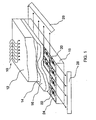
- Fig. 1 illustrates an embodiment of the present invention wherein an x-ray beam 10 is directed onto the x-ray conversion scintillator 12 which, for example, may be made of CsI.
- Such scintillator is typically 300-500 ⁇ m thick and it absorbs about 80% -90% of incoming radiation while converting x-rays into light.
- a light transparent top biasing electrode 14 which can be made of materials such as ITO.
- the present invention provides a co-planar thin (e.g. 5-20 ⁇ m) layer of photosensitive selenium based photoreceptor 16 having a multilayer structure which converts light into electrical charges.
- This photosensitive layer 16 is deposited onto an active matrix substrate 18 comprising arrays of TFT switches 20, storage capacitors 22 and conduction pads 24.
- Such TFTs may also be replaced by switching diodes (not shown).
- the substrate 18 is also provided, as is known in the art, with line by line scanning circuits 26 and read out circuits 28.
- the scintillator 12 and the selenium photosensitive multilayer photoreceptor 16 are enclose the scintillator 12 and the selenium photosensitive multilayer photoreceptor 16 as well as the biasing electrode 14, within a suitable housing (not shown) to provide environmental, electrical and mechanical protection therefor.
- the indices of refraction of the scintillator and of the selenium multilayer may be suitably matched, making use of the light transparent biasing electrode.
- the means for biasing the detector to apply an electric field strength of between 5 and 50 V/ ⁇ m across the selenium based multilayer structure having again of close to 1, with no avalanche multiplication. This allows the detector to operate under very high dose rates without having to saturate the output amplifiers.
- the active matrix is a two-dimensional array of thin film transistors (TFTs) made, for example, of amorphous silicon.
- TFTs thin film transistors
- Each TFT is normally associated with a storage capacitance which is usually part of the TFT architecture.
- Such active matrix is covered with a photoreceptor made of a photosensitive n-i-p or p-i-n multilayer structure (the p-i-n multilayer structure does not form part of the invention) comprising: (1) a thin ( ⁇ 1 ⁇ m) selenium hole blocking n-layer doped with a material such as an alkaline metal (e.g.
- a transparent co-planar biasing electrode which may consist of indium tin oxide (ITO).
- the i-layer of amorphous selenium doped with chlorine and arsenic may contain 1-100 ppm of chlorine and 0.1-5% by wt. of arsenic and the p-layer of arsenic enriched a-Se may contain 1-38% by wt. of arsenic.
- the hole blocking n-layer and the electron blocking p-layer may be made of any suitable material producing the desired hole blocking and electron blocking effect, however, the middle i-layer must be made of amorhpous selenium doped with chlorine and arsenic.
- n-i-p the hole blocking n-layer is adjacent to the scintillator and the electron blocking p-layer is adjacent to the active matrix
- p-in the reverse is true, namely the n-layer is adjacent to the active matrix, while the p-layer is adjacent to the scintillator.
- the selenium structure comprises an "n” hole blocking layer deposited on the active surface of the TFT matrix, thus making contact with conduction pads on said matrix.
- an electron blocking "p” layer is provided which is transparent to the light generated by the scintillator.
- An amorphous selenium “i” layer is sandwiched in between the "n” and the "p” layers.
- the top electrode is maintained herein at a negative potential with respect to the pads periodically connected to the near ground potential of the drain electrode of the TFTs.
- the biasing electrode is at a positive potential.
- a protective device should be inserted between the pad and the biasing electrode to avoid the pad potential to grow positively beyond an allowable voltage and destroy the TFT. This could happen, for instance, under severe overexposure.
- the voltage protection device could be made of an amorphous silicon TFT shunting the storage capacitance.
- a storage capacitance is normally associated with each TFT switch, however if the selenium layer is thin enough to provide a proper charge storage, the storage capacitance will then be an integral part of such photoreceptor.
- the scintillator is preferably made of a blue light emission material such as cesium iodide doped with sodium (0.1 - 5% by wt.), rather than thallium, in order to produce, under the x-ray irradiation, a color glow matching the maximum photosensitivity of the selenium.
- the scintillator layer is made of materials such as calcium tungstate, barium fluoride or sodium iodide, emitting light in the blue spectrum.
- the role of the selenium multilayer is two-fold. Firstly, it acts as the light absorber layer thereby converting the incident energy into electrical charges proportional to the intensity level of the incident radiation. Secondly, it acts as the charge transport layer whereby the generated carriers are transported under the effect of an applied electric field to the underlying pixelated electrode.
- the thickness of the selenium multilayer is much less than the width of a pixel electrode so that in association with the direction of the electric field and the high intrinsic resistance of selenium, the lateral spread of charge is minimized.
- the selenium based multilayer is preferably optimized for electrical transport where the dark current is below 200 pA/cm 2 , preferably below 100 pA/cm 2 and the residual image is less than 5%, preferably less than 1%. This is achieved by proper control of the compositions and thicknesses of the individual layers of the photoreceptor.
- the scintillator layer is deposited directly onto a combined monolithic structure consisting of the biasing electrode, the co-planar selenium based multilayer photoreceptor and the active TFT matrix.
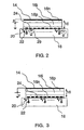
- Fig. 2 illustrates a n-i-p structure where the common electrode 14 is under positive bias.
- electron blocking layer 16p made of selenium doped with arsenic and having a thickness of a few nanometers is deposited; then is provided layer 16i of several tens of microns of selenium doped with chlorine and arsenic, and finally hole blocking layer 16n having a thickness of a few nanometers, is deposited just under the electrode 14.
- Such n-i-p structure is provided with a protective high voltage device 29 which is inserted between the pad 24 and the biasing electrode 14 to avoid the pad potential to grow beyond an allowable voltage and destroy the TFTs. This could happen, for instance, in the event of severe overexposure.
- Fig. 3 illustrates a p-i-n arrangement of the selenium multilayer photoreceptor 16 on top of which there is provided the light-transparent biasing electrode 14 which is biased to a negative potential.
- the thin hole blocking layer 16n is deposited on conduction pads 24 of the active matrix substrate 18 of TFT arrays comprising TFT switch elements 20 and storage capacitors 22.
- the thin electron blocking layer 16p is located on the side of the biasing electrode 14 and is transparent to the light generated by the scintillator 12.
- the "i” layer 16i of this p-i-n structure, which is sandwiched between the "n” and “p” layers is a thin amorphous selenium layer doped with arsenic and chlorine.
- the "i” layer is typically 10 to 20 ⁇ m thick
- This selenium multilayer structure 16 acts as a light absorber thereby converting the incident light into electrical charges proportional to the intensity level of the incident radiation and secondly it acts as a charge transport layer whereby the generated electrical charges are transported under the effect of the applied electric field to the underlying pixelated electrode 18.
- the top electrode 14 is herein at a negative potential with respect to the pads 24 periodically connected to the near ground potential on the drain electrode of the TFTs. Such a structure need not be protected against high voltage discharge since the TFT 18 will become conducting should the pad 24 voltage reach the negative bias of the TFT gate.
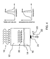
- Fig. 4 illustrates the method of x-ray detection with a p-i-n detector structure shown in Fig. 3 .
- the x-ray beam 10 is directed to and passes through scintillator 12 which may be made, for example, of a thick layer of cesium iodide doped with sodium, and where about 80% of incoming x-ray irradiation is absorbed, and by which the x-rays are converted into light.
- the light signal 30 emitted by the scintillator 12 is then passed through transparent top electrode 14 and the co-planar selenium multilayer 16 which, in this case, has a p-i-n structure.
- the peak of the light signal emitted by the scintillator is at a wavelength of 420 nm.
- the wavelength of the emitted light coming from the scintillator 12 is made to match the maximum photoresponse of the selenium multilayer 16.
- the selenium multilayer 16 is deposited on conduction pads 24 of TFT matrix provided with TFT switching elements 20 and storage capacitors 22. Such TFT matrix may, if desired, be replaced by switching diodes.
- a high voltage protective device would be required within the TFT matrix as shown in Fig. 2 .
Landscapes
- Engineering & Computer Science (AREA)
- Power Engineering (AREA)
- Physics & Mathematics (AREA)
- General Physics & Mathematics (AREA)
- Electromagnetism (AREA)
- Condensed Matter Physics & Semiconductors (AREA)
- Health & Medical Sciences (AREA)
- Toxicology (AREA)
- Computer Hardware Design (AREA)
- Microelectronics & Electronic Packaging (AREA)
- Solid State Image Pick-Up Elements (AREA)
- Measurement Of Radiation (AREA)
- Apparatus For Radiation Diagnosis (AREA)
- Light Receiving Elements (AREA)
Description
- This invention relates to an indirect x-ray image detector suitable for radiology. The term "indirect" means that the x-rays are not directly converted into electrical charges, but rather they are first converted into light using a scintillator, and then light is converted into electrical charges by appropriate means. More particularly, this invention relates to an x-ray detector where the usual array of pixelated photodiodes used to convert light into electrical charges, is replaced by a photoreceptor formed of a thin uniform layer of photosensitive selenium having a multilayer structure.
- It is well known to produce indirect x-ray image detectors based on a system comprising a thin film transistor (TFT) matrix deposited on a glass substrate and a corresponding array of photodiodes with an inherent capacitor, as well as an electrode connected to the source of the TFT. The photodiodes are covered with a common transparent electrode and a scintillator. Scanning circuits are connected to the lines of the TFT array while reading circuits are connected to the columns of the TFT matrix.
- In such known devices, initially, all the free electrodes of the photodiodes are biased at the same reference voltage. The detector undergoes an exposure. Light is generated in the scintillator which causes the photodiodes to generate and leak charges. The associated capacitance of each photodiode releases a charge proportional to the local exposure resulting in a charge topography over the entire detector. The scanning circuits scan the lines in sequence switching the TFTs and successively connecting the free electrode of each photodiode-capacitance on the active line to the virtual reference voltage of the columns. These columns are connected to a read-out preamplifier which integrates the charge required to bring back the photodiodes to the reference potential. During the time of a line connection, the readout circuit on each line processes the integrated charges and multiplexes them to an output buffer memory where the entire two dimensional image builds up. In these arrangements, the TFTs can also be replaced by switching diodes. Such TFTs or switching diodes and photodiodes are generally made of amorphous silicon. TFTs can also be made of CdSe material. The scintillator is generally made of evaporated CsI.
- One such prior art arrangement using a scintillator detector crystal, preferably made of a thallium doped cesium iodide crystal, and an array of photodiodes arranged to receive the scintillator photons, is disclosed in
U.S. Patent No. 5,171,998 of Engdahl et al., for gamma ray imaging. - Another prior art arrangement is disclosed in
U.S. Patent No. 5,198,673 of Rougeot et al. where a scintillator is optically coupled to a large area photosensor which is disposed on a substrate and is electrically coupled to a data read and reset circuit. The large area photosensor is provided with an amorphous selenium photosensitive material that exhibits avalanche multiplication gain when a selected high biasing voltage is applied, but which does not have a multilayer structure and requires a biasing voltage between 100V and 1000V to cause the photosensor to exhibit avalanche multiplication. In this patent, there is also included a protective TFT coupled to the data read and reset circuit to provide overvoltage protection from the high biasing voltage. - A further prior art detector is disclosed in
U.S. Patent No. 4,363,909 of Ong where an array of optically isolated small area scintillators overlay a duophotoconductive sandwich structure that includes a photoconductive layer which acts as a switch. Both photoconductive layers can be made of amorphous selenium. This system uses a duo-dielectric sandwich structure, but does not use an active matrix substrate such as a TFT. Also, the construction of an array of scintillators is a complex and difficult task which has not achieved widespread application. - A still further prior art x-ray detector is disclosed in
U.S. Patent No. 5,464,984 of Cox et al. It includes a scintillator, a sensor array of silicon-on- insulator substrate (SOI), processing circuits and a ceramic layer which overlays the processing circuits. No photosensitive selenium is, however, used in this patent. - Also,
U.S. patent No. 5,585,638 of Hoffman discloses an x-ray detector assembly that comprises an imaging device formed by a scintillator in front of a two-dimensional photodetector array. The active layers are formed on a surface of substrate and a uniform first electrode layer is applied over the entire major surface on one side of the substrate and serves as a high voltage bias electrode. Then, a thin semiconductive layer which constitutes a second electrode, extends over the first electrode layer and provides an electrical characteristic that varies in response to impingement of x-rays. Again, no photosensitive selenium is used therein. - An x-ray detector is disclosed in
US5,396,072 which comprises a number of sensors. Each sensor comprises a collecting electrode and a photoconductor having a multilayer structure of a p-i-n type with the p-type layer acting as a electron blocking layer and with the n-type layer acting as a hole blocking layer. The thickness of the multilayer structure is 201.5 - 807 µm. - Such prior art devices present a number of disadvantages in terms of high cost and poor resolution. Also, they may be operated only by application of either high voltage or low voltage, thereby restricting their field of use.
- It is the object of the present invention to provide an improvement to the known systems by replacing the array of photodiodes or other photosensors used in the prior art by a photoreceptor formed of a uniform thin layer of photosensitive selenium having a multilayer structure, which leads to many important advantages.
- In essence, the present invention provides an indirect x-ray image detector as disclosed in claim 1.
- A non-limitative embodiment of the present invention will now be described with reference to the appended drawings, in which:
-
Fig. 1 is a perspective diagrammatical view of a structure of a detector in accordance with this invention; -
Fig. 2 is a diagrammatic side view of a n-i-p photoreceptor layer on TFT matrix, with a high voltage protection device; and -
Fig. 3 is a diagrammatic side view of a p-i-n photoreceptor layer on TFT matrix, which requires no high voltage protection; -
Fig. 4 is a diagrammatic view of a combination of the scintillator and a-Se photoreceptor with graphs showing the scintillator emitted light signal wavelength curve and the selenium photoresponse wavelength curve. - In the Figures, the same elements are identified by the same reference numbers.
-
Fig. 1 illustrates an embodiment of the present invention wherein anx-ray beam 10 is directed onto thex-ray conversion scintillator 12 which, for example, may be made of CsI. Such scintillator is typically 300-500 µm thick and it absorbs about 80% -90% of incoming radiation while converting x-rays into light. Under thescintillator 12, there is provided a light transparenttop biasing electrode 14 which can be made of materials such as ITO. Under thisbiasing electrode 14, the present invention provides a co-planar thin (e.g. 5-20 µm) layer of photosensitive selenium basedphotoreceptor 16 having a multilayer structure which converts light into electrical charges. Thisphotosensitive layer 16 is deposited onto anactive matrix substrate 18 comprising arrays ofTFT switches 20,storage capacitors 22 andconduction pads 24. Such TFTs may also be replaced by switching diodes (not shown). - The
substrate 18 is also provided, as is known in the art, with line byline scanning circuits 26 and read outcircuits 28. - It is preferable to enclose the
scintillator 12 and the seleniumphotosensitive multilayer photoreceptor 16 as well as thebiasing electrode 14, within a suitable housing (not shown) to provide environmental, electrical and mechanical protection therefor. - The indices of refraction of the scintillator and of the selenium multilayer may be suitably matched, making use of the light transparent biasing electrode. The means for biasing the detector to apply an electric field strength of between 5 and 50 V/µm across the selenium based multilayer structure having again of close to 1, with no avalanche multiplication. This allows the detector to operate under very high dose rates without having to saturate the output amplifiers.
- In accordance with a preferred embodiment of this invention, the active matrix is a two-dimensional array of thin film transistors (TFTs) made, for example, of amorphous silicon. Each TFT is normally associated with a storage capacitance which is usually part of the TFT architecture. Such active matrix is covered with a photoreceptor made of a photosensitive n-i-p or p-i-n multilayer structure (the p-i-n multilayer structure does not form part of the invention) comprising: (1) a thin (< 1µm) selenium hole blocking n-layer doped with a material such as an alkaline metal (e.g. lithium, sodium, potassium or cesium) or an oxide or halogenide of such metal; (2) an amorphous selenium i-layer doped with chlorine and arsenic and (3) a final thin (< 1µm) electron blocking p-layer of arsenic enriched amorphous selenium. On top of this multilayer structure there is placed a transparent co-planar biasing electrode, which may consist of indium tin oxide (ITO).
- The i-layer of amorphous selenium doped with chlorine and arsenic may contain 1-100 ppm of chlorine and 0.1-5% by wt. of arsenic and the p-layer of arsenic enriched a-Se may contain 1-38% by wt. of arsenic. It should be pointed out that within the scope of the present invention, the hole blocking n-layer and the electron blocking p-layer may be made of any suitable material producing the desired hole blocking and electron blocking effect, however, the middle i-layer must be made of amorhpous selenium doped with chlorine and arsenic.
- In the "n-i-p" structure the hole blocking n-layer is adjacent to the scintillator and the electron blocking p-layer is adjacent to the active matrix, whereas in the "p-in" structure the reverse is true, namely the n-layer is adjacent to the active matrix, while the p-layer is adjacent to the scintillator.
- In the p-i-n arrangement (which does not form part of the invention), the selenium structure comprises an "n" hole blocking layer deposited on the active surface of the TFT matrix, thus making contact with conduction pads on said matrix. On the scintillator side, an electron blocking "p" layer is provided which is transparent to the light generated by the scintillator. An amorphous selenium "i" layer is sandwiched in between the "n" and the "p" layers. The top electrode is maintained herein at a negative potential with respect to the pads periodically connected to the near ground potential of the drain electrode of the TFTs. Such a structure need not be protected against high voltage discharge since the TFTs will become conducting should the pad voltage reach the negative bias of the TFT gate.
- In the alternate n-i-p structure, the biasing electrode is at a positive potential. Here, a protective device should be inserted between the pad and the biasing electrode to avoid the pad potential to grow positively beyond an allowable voltage and destroy the TFT. This could happen, for instance, under severe overexposure. The voltage protection device could be made of an amorphous silicon TFT shunting the storage capacitance.
- A storage capacitance is normally associated with each TFT switch, however if the selenium layer is thin enough to provide a proper charge storage, the storage capacitance will then be an integral part of such photoreceptor.
- The scintillator is preferably made of a blue light emission material such as cesium iodide doped with sodium (0.1 - 5% by wt.), rather than thallium, in order to produce, under the x-ray irradiation, a color glow matching the maximum photosensitivity of the selenium. According to the invention, the scintillator layer is made of materials such as calcium tungstate, barium fluoride or sodium iodide, emitting light in the blue spectrum.
- According to this invention, the role of the selenium multilayer is two-fold. Firstly, it acts as the light absorber layer thereby converting the incident energy into electrical charges proportional to the intensity level of the incident radiation. Secondly, it acts as the charge transport layer whereby the generated carriers are transported under the effect of an applied electric field to the underlying pixelated electrode. The thickness of the selenium multilayer is much less than the width of a pixel electrode so that in association with the direction of the electric field and the high intrinsic resistance of selenium, the lateral spread of charge is minimized.
- The selenium based multilayer is preferably optimized for electrical transport where the dark current is below 200 pA/cm2, preferably below 100 pA/cm2 and the residual image is less than 5%, preferably less than 1%. This is achieved by proper control of the compositions and thicknesses of the individual layers of the photoreceptor.
- Moreover, according to the present invention, the scintillator layer is deposited directly onto a combined monolithic structure consisting of the biasing electrode, the co-planar selenium based multilayer photoreceptor and the active TFT matrix.
-
Fig. 2 illustrates a n-i-p structure where thecommon electrode 14 is under positive bias. Here, on top of theTFT array 18 and the metal orITO pads 24,electron blocking layer 16p made of selenium doped with arsenic and having a thickness of a few nanometers is deposited; then is providedlayer 16i of several tens of microns of selenium doped with chlorine and arsenic, and finally hole blockinglayer 16n having a thickness of a few nanometers, is deposited just under theelectrode 14. Such n-i-p structure is provided with a protectivehigh voltage device 29 which is inserted between thepad 24 and the biasingelectrode 14 to avoid the pad potential to grow beyond an allowable voltage and destroy the TFTs. This could happen, for instance, in the event of severe overexposure. -
Fig. 3 illustrates a p-i-n arrangement of theselenium multilayer photoreceptor 16 on top of which there is provided the light-transparent biasing electrode 14 which is biased to a negative potential. Here the thinhole blocking layer 16n is deposited onconduction pads 24 of theactive matrix substrate 18 of TFT arrays comprisingTFT switch elements 20 andstorage capacitors 22. The thinelectron blocking layer 16p is located on the side of the biasingelectrode 14 and is transparent to the light generated by thescintillator 12. These "n" and "p" layers are typically a few nanometers in thickness. - The "i"
layer 16i of this p-i-n structure, which is sandwiched between the "n" and "p" layers is a thin amorphous selenium layer doped with arsenic and chlorine. The "i" layer is typically 10 to 20 µm thick Thisselenium multilayer structure 16 acts as a light absorber thereby converting the incident light into electrical charges proportional to the intensity level of the incident radiation and secondly it acts as a charge transport layer whereby the generated electrical charges are transported under the effect of the applied electric field to the underlyingpixelated electrode 18. Thetop electrode 14 is herein at a negative potential with respect to thepads 24 periodically connected to the near ground potential on the drain electrode of the TFTs. Such a structure need not be protected against high voltage discharge since theTFT 18 will become conducting should thepad 24 voltage reach the negative bias of the TFT gate. -
Fig. 4 illustrates the method of x-ray detection with a p-i-n detector structure shown inFig. 3 . As shown in thisFig. 4 , thex-ray beam 10 is directed to and passes throughscintillator 12 which may be made, for example, of a thick layer of cesium iodide doped with sodium, and where about 80% of incoming x-ray irradiation is absorbed, and by which the x-rays are converted into light. Thelight signal 30 emitted by thescintillator 12 is then passed through transparenttop electrode 14 and theco-planar selenium multilayer 16 which, in this case, has a p-i-n structure. The top graph shown inFig. 4 indicates that the peak of the light signal emitted by the scintillator is at a wavelength of 420 nm. In this case, the wavelength of the emitted light coming from thescintillator 12 is made to match the maximum photoresponse of theselenium multilayer 16. - The
selenium multilayer 16 is deposited onconduction pads 24 of TFT matrix provided withTFT switching elements 20 andstorage capacitors 22. Such TFT matrix may, if desired, be replaced by switching diodes. - In the case of the set-up shown in
Fig. 4 , in operation thetop electrode 14 is placed under negative potential with respect to thepads 24 which are connected to the ground throughcapacitors 22. In this manner, no protection against high voltage discharge is needed since the TFT will become conducting should the pad voltage reach the negative bias of the TFT gate. - The selenium photoresponse produced by the
multilayer 16, as shown in the bottom graph inFig. 4 , is matched to the wavelength peak at 420 nm, emitted by the scintillator. As a result, the output photocurrent, which is directly proportional to the emitted light signal, is optimized. - If instead of a p-i-n structure, a n-i-p structure of the
selenium multilayer 16 is used, then a high voltage protective device would be required within the TFT matrix as shown inFig. 2 .
Claims (9)
- An indirect x-ray image detector suitable for radiology, comprising an active matrix substrate (18) with scanning and read-out circuits, wherein over said active matrix substrate there is deposited a photoreceptor (16) made of a co-planar layer of amorphous selenium based multilayer structure having a thickness of between 2 and 50µm, said photoreceptor (16) being covered with a light-transparent biasing electrode (14) on top of which there is provided an x-ray conversion scintillator (12),
and the scintillator (12) is made of a material selected from cesium iodide doped with sodium, barium fluoride, calcium tungstate and sodium iodide, emitting in the blue spectrum, characterised in that the amorphous selenium based multilayer structure is of n-i-p type, wherein the n-layer (16n) is a hole blocking layer, the p-layer (16p) is an electron blocking layer and the i-layer sandwiched between the n and p layers is an amorphous selenium layer doped with chlorine and arsenic, and the p-layer (16p) is adjacent to the active matrix substrate (18), and means are provided for biasing the detector to apply an electric field strength of between 5 and 50 V/µm across the selenium based multilayer structure so as to operate the structure with no avalanche multiplication. - An x-ray image detector according to claim 1, in which the active matrix substrate (18) is a two dimensional array of thin film transistors (TFT) (20) associated with a storage capacitance (22) and having conduction pads (24) with electric connection to the photoreceptor (16).
- An x-ray image detector according to claim 2, in which the storage capacitance (22) is a part of the TFT architecture.
- An x-ray image detector according to claim 2, in which the storage capacitance (22) is an integral part of the photoreceptor (16).
- An x-ray image detector according to claim 2, 3 or 4, in which the TFT (20) are made of amorphous silicon.
- An x-ray image detector according to any one of claims 1 to 5, wherein the i-layer (16i) of amorphous selenium is doped with 1-100 ppm of chlorine and 0.1 - 5% by wt. of arsenic.
- An x-ray image detector according to any one of claims 1 to 5, in which the n-layer (16n) is a selenium layer doped with an alkaline metal or an oxide or halogenide of said metal and having a thickness of less than 1 µm.
- An x-ray image detector according to claim 7, in which the alkaline metal is selected from lithium, sodium, potassium and cesium.
- An x-ray image detector according to any one of claims 1 to 8, in which the p-layer (16p) is a layer of arsenic enriched amorphous selenium having a thickness of less than 1µm.
Applications Claiming Priority (2)
| Application Number | Priority Date | Filing Date | Title |
|---|---|---|---|
| CA2241779A CA2241779C (en) | 1998-06-26 | 1998-06-26 | Indirect x-ray image detector for radiology |
| CA2241779 | 1998-06-26 |
Publications (3)
| Publication Number | Publication Date |
|---|---|
| EP0967655A2 EP0967655A2 (en) | 1999-12-29 |
| EP0967655A3 EP0967655A3 (en) | 2000-06-28 |
| EP0967655B1 true EP0967655B1 (en) | 2009-12-09 |
Family
ID=4162593
Family Applications (1)
| Application Number | Title | Priority Date | Filing Date |
|---|---|---|---|
| EP99304399A Expired - Lifetime EP0967655B1 (en) | 1998-06-26 | 1999-06-07 | Indirect x-ray image detector for radiology |
Country Status (5)
| Country | Link |
|---|---|
| US (2) | US6982425B1 (en) |
| EP (1) | EP0967655B1 (en) |
| JP (1) | JP2000035480A (en) |
| CA (1) | CA2241779C (en) |
| DE (1) | DE69941758D1 (en) |
Families Citing this family (28)
| Publication number | Priority date | Publication date | Assignee | Title |
|---|---|---|---|---|
| CA2241779C (en) * | 1998-06-26 | 2010-02-09 | Ftni Inc. | Indirect x-ray image detector for radiology |
| CA2242743C (en) * | 1998-07-08 | 2002-12-17 | Ftni Inc. | Direct conversion digital x-ray detector with inherent high voltage protection for static and dynamic imaging |
| FR2803394B1 (en) * | 1999-12-30 | 2003-04-25 | Thomson Tubes Electroniques | X-RAY IMAGE DETECTION SYSTEM FOR SCANNING X-RAY GENERATOR |
| AU2001244586A1 (en) * | 2000-04-04 | 2001-10-15 | Hamamatsu Photonics K.K. | Semiconductor energy detector |
| JP2002286847A (en) * | 2001-03-22 | 2002-10-03 | Reitekku:Kk | Semiconductor radiation detector |
| US6730900B2 (en) * | 2002-02-05 | 2004-05-04 | E-Phocus, Inc. | Camera with MOS or CMOS sensor array |
| JP4391079B2 (en) * | 2002-11-28 | 2009-12-24 | 浜松ホトニクス株式会社 | Solid-state imaging device and radiation imaging device |
| JP2005012049A (en) * | 2003-06-20 | 2005-01-13 | Shimadzu Corp | Radiation detector and radiation pickup device equipped therewith |
| KR20070107137A (en) * | 2005-02-28 | 2007-11-06 | 오씨 외를리콘 발처스 악티엔게젤샤프트 | Method of fabrication an image sensor device with reduced pixel cross-talk |
| US7291842B2 (en) * | 2005-06-14 | 2007-11-06 | Varian Medical Systems Technologies, Inc. | Photoconductor imagers with sandwich structure |
| DE102005037290A1 (en) * | 2005-08-08 | 2007-02-22 | Siemens Ag | Flat panel detector |
| US7795592B2 (en) | 2005-11-21 | 2010-09-14 | Fujifilm Corporation | Image detector and manufacturing method of the same |
| JP4762692B2 (en) * | 2005-11-21 | 2011-08-31 | 富士フイルム株式会社 | Radiation image detector and method for manufacturing radiation image detector |
| JP2008227036A (en) * | 2007-03-12 | 2008-09-25 | Fujifilm Corp | Radiation plane detector |
| KR101497498B1 (en) | 2008-12-19 | 2015-03-03 | 삼성전자주식회사 | Method and appratus for acquiring penetration images of radioactive ray |
| KR101634250B1 (en) | 2010-06-21 | 2016-06-28 | 삼성전자주식회사 | Large-scaled x-ray detector and method of manufacturing the same |
| JP2012229999A (en) * | 2011-04-26 | 2012-11-22 | Fujifilm Corp | Radiation image detecting device and radiographic apparatus |
| US8445853B2 (en) | 2011-08-22 | 2013-05-21 | Eastman Kodak Company | Method of making a radiation-sensitive substrate |
| US8530848B2 (en) | 2011-08-22 | 2013-09-10 | Eastman Kodak Company | Radiation-sensitive substrate |
| US8745861B2 (en) | 2012-04-25 | 2014-06-10 | Eastman Kodak Company | Method of making a storage system having an environmentally-modifiable conductor |
| US8356758B1 (en) | 2012-04-25 | 2013-01-22 | Eastman Kodak Company | Making storage system having modifiable conductor and memory |
| US8739399B2 (en) | 2012-04-25 | 2014-06-03 | Eastman Kodak Company | Making electronic storage system having code circuit |
| JP6099035B2 (en) * | 2012-10-12 | 2017-03-22 | Nltテクノロジー株式会社 | Photoelectric conversion device, method of manufacturing the same, and X-ray image detection device |
| CN109863599A (en) | 2016-11-30 | 2019-06-07 | 纽约州州立大学研究基金会 | Mix active matrix flat-panel detector system and method |
| JP7167060B2 (en) | 2017-05-01 | 2022-11-08 | コーニンクレッカ フィリップス エヌ ヴェ | multilayer detector |
| EP3495849A1 (en) * | 2017-12-11 | 2019-06-12 | Koninklijke Philips N.V. | Multilayer pixelated scintillator with enlarged fill factor |
| TWI652945B (en) | 2017-12-20 | 2019-03-01 | 財團法人工業技術研究院 | Radiation imager with automatic exposure detection capability and method thereof |
| FR3119708B1 (en) * | 2021-02-11 | 2023-08-25 | Trixell | Digital detector with superimposed conversion stages |
Family Cites Families (25)
| Publication number | Priority date | Publication date | Assignee | Title |
|---|---|---|---|---|
| US4230510A (en) * | 1977-11-21 | 1980-10-28 | General Electric Company | Distributed phosphor scintillator structures |
| US4363969A (en) | 1980-07-16 | 1982-12-14 | Ong Poen S | Light switched segmented tomography detector |
| US4883956A (en) * | 1985-12-23 | 1989-11-28 | Schlumberger Technology Corporation | Methods and apparatus for gamma-ray spectroscopy and like measurements |
| EP0338091A4 (en) * | 1987-10-21 | 1992-12-09 | Hitachi, Ltd. | Light-receiving element and method of operating the same |
| US5196702A (en) * | 1987-10-21 | 1993-03-23 | Hitachi, Ltd. | Photo-sensor and method for operating the same |
| JP2686266B2 (en) * | 1988-01-28 | 1997-12-08 | 株式会社日立製作所 | Manufacturing method of light receiving element |
| US5039858A (en) * | 1990-01-31 | 1991-08-13 | Anderson David F | Divalent fluoride doped cerium fluoride scintillator |
| US5171998A (en) | 1990-06-14 | 1992-12-15 | Engdahl John C | Gamma ray imaging detector |
| US5132539A (en) * | 1991-08-29 | 1992-07-21 | General Electric Company | Planar X-ray imager having a moisture-resistant sealing structure |
| US5198673A (en) * | 1992-01-23 | 1993-03-30 | General Electric Company | Radiation image detector with optical gain selenium photosensors |
| DE4227096A1 (en) * | 1992-08-17 | 1994-02-24 | Philips Patentverwaltung | X-ray image detector |
| JPH0763859A (en) * | 1993-08-27 | 1995-03-10 | Shimadzu Corp | Two-dimensional detector of radiation |
| US5515411A (en) | 1993-03-31 | 1996-05-07 | Shimadzu Corporation | X-ray image pickup tube |
| JPH08509550A (en) * | 1993-04-28 | 1996-10-08 | ユニバーシティ オブ サリー | Radiation detector |
| US5596198A (en) * | 1994-04-22 | 1997-01-21 | The Regents, University Of California | Gamma ray camera |
| GB9414639D0 (en) * | 1994-07-20 | 1994-09-07 | Philips Electronics Uk Ltd | An image detector |
| EP0823132B1 (en) | 1995-04-28 | 1999-08-04 | Sunnybrook Hospital | Active matrix x-ray imaging array |
| JPH09331051A (en) * | 1995-06-16 | 1997-12-22 | S I I R D Center:Kk | Photoelectric conversion semiconductor device |
| US5585638A (en) | 1995-12-14 | 1996-12-17 | General Electric Company | X-ray detector for automatic exposure control of an imaging apparatus |
| US5892222A (en) * | 1996-04-18 | 1999-04-06 | Loral Fairchild Corporation | Broadband multicolor photon counter for low light detection and imaging |
| JPH1065136A (en) * | 1996-08-13 | 1998-03-06 | Dainippon Printing Co Ltd | Optical sensor, apparatus for recording information and method for recording and reproducing information |
| CA2184667C (en) * | 1996-09-03 | 2000-06-20 | Bradley Trent Polischuk | Multilayer plate for x-ray imaging and method of producing same |
| DE19640946A1 (en) * | 1996-10-04 | 1998-04-16 | Philips Patentverwaltung | X-ray arrangement with a photoconductor |
| JPH10197647A (en) * | 1997-01-14 | 1998-07-31 | Toshiba Corp | X-ray image detector |
| CA2241779C (en) * | 1998-06-26 | 2010-02-09 | Ftni Inc. | Indirect x-ray image detector for radiology |
-
1998
- 1998-06-26 CA CA2241779A patent/CA2241779C/en not_active Expired - Lifetime
-
1999
- 1999-06-07 EP EP99304399A patent/EP0967655B1/en not_active Expired - Lifetime
- 1999-06-07 DE DE69941758T patent/DE69941758D1/en not_active Expired - Lifetime
- 1999-06-17 US US09/334,671 patent/US6982425B1/en not_active Expired - Lifetime
- 1999-06-25 JP JP11180725A patent/JP2000035480A/en active Pending
-
2005
- 2005-10-04 US US11/242,574 patent/US7692157B2/en not_active Expired - Fee Related
Also Published As
| Publication number | Publication date |
|---|---|
| JP2000035480A (en) | 2000-02-02 |
| US20060027760A1 (en) | 2006-02-09 |
| CA2241779A1 (en) | 1999-12-26 |
| CA2241779C (en) | 2010-02-09 |
| DE69941758D1 (en) | 2010-01-21 |
| EP0967655A2 (en) | 1999-12-29 |
| EP0967655A3 (en) | 2000-06-28 |
| US7692157B2 (en) | 2010-04-06 |
| US6982425B1 (en) | 2006-01-03 |
Similar Documents
| Publication | Publication Date | Title |
|---|---|---|
| US7692157B2 (en) | Indirect x-ray image detector for radiology | |
| US5198673A (en) | Radiation image detector with optical gain selenium photosensors | |
| US5420452A (en) | Solid state radiation detector | |
| US7773139B2 (en) | Image sensor with photosensitive thin film transistors | |
| US8785867B2 (en) | Radiation detector, imaging device and electrode structure thereof, and method for acquiring an image | |
| US7541617B2 (en) | Radiation image pickup device | |
| TWI470262B (en) | Radiographic detector formed on scintillator | |
| US9136296B2 (en) | Photoelectric conversion apparatus and radiographic imaging apparatus | |
| EP1206125A2 (en) | Radiation image pick-up device | |
| CA2669678C (en) | Photodetector/imaging device with avalanche gain | |
| CA2233816A1 (en) | High resolution, low voltage flat-panel radiation imaging sensors | |
| CN201852941U (en) | Radiation detector and imaging device and electrode structure thereof | |
| KR20140001968A (en) | Apparatus and methods for high performance radiographic imaging array including reflective capability | |
| US6515286B2 (en) | Solid-state radiation detector in which signal charges are reduced below saturation level | |
| EP0686268B1 (en) | Low noise solid state fluorscopic radiation imager | |
| US7233003B2 (en) | Radiation detector | |
| JP2004096079A (en) | Photoelectric converter, image reader, and manufacturing method of photoelectric converter | |
| US20110284749A1 (en) | Radiation detector | |
| US6373062B1 (en) | Interdigital photodetector for indirect x-ray detection in a radiography imaging system | |
| JPH0763859A (en) | Two-dimensional detector of radiation | |
| CN114864609A (en) | Active pixel sensor and flat panel detector |
Legal Events
| Date | Code | Title | Description |
|---|---|---|---|
| PUAI | Public reference made under article 153(3) epc to a published international application that has entered the european phase |
Free format text: ORIGINAL CODE: 0009012 |
|
| AK | Designated contracting states |
Kind code of ref document: A2 Designated state(s): BE CH DE DK FR GB IT LI NL SE |
|
| AX | Request for extension of the european patent |
Free format text: AL;LT;LV;MK;RO;SI |
|
| PUAL | Search report despatched |
Free format text: ORIGINAL CODE: 0009013 |
|
| AK | Designated contracting states |
Kind code of ref document: A3 Designated state(s): AT BE CH CY DE DK ES FI FR GB GR IE IT LI LU MC NL PT SE |
|
| AX | Request for extension of the european patent |
Free format text: AL;LT;LV;MK;RO;SI |
|
| RIC1 | Information provided on ipc code assigned before grant |
Free format text: 7H 01L 27/146 A, 7G 01T 1/24 B |
|
| 17P | Request for examination filed |
Effective date: 20001211 |
|
| AKX | Designation fees paid |
Free format text: BE CH DE DK FR GB IT LI NL SE |
|
| GRAP | Despatch of communication of intention to grant a patent |
Free format text: ORIGINAL CODE: EPIDOSNIGR1 |
|
| GRAS | Grant fee paid |
Free format text: ORIGINAL CODE: EPIDOSNIGR3 |
|
| GRAA | (expected) grant |
Free format text: ORIGINAL CODE: 0009210 |
|
| AK | Designated contracting states |
Kind code of ref document: B1 Designated state(s): BE CH DE DK FR GB IT LI NL SE |
|
| REG | Reference to a national code |
Ref country code: GB Ref legal event code: FG4D |
|
| REG | Reference to a national code |
Ref country code: CH Ref legal event code: EP |
|
| REF | Corresponds to: |
Ref document number: 69941758 Country of ref document: DE Date of ref document: 20100121 Kind code of ref document: P |
|
| REG | Reference to a national code |
Ref country code: NL Ref legal event code: T3 |
|
| PG25 | Lapsed in a contracting state [announced via postgrant information from national office to epo] |
Ref country code: SE Free format text: LAPSE BECAUSE OF FAILURE TO SUBMIT A TRANSLATION OF THE DESCRIPTION OR TO PAY THE FEE WITHIN THE PRESCRIBED TIME-LIMIT Effective date: 20091209 |
|
| PG25 | Lapsed in a contracting state [announced via postgrant information from national office to epo] |
Ref country code: BE Free format text: LAPSE BECAUSE OF FAILURE TO SUBMIT A TRANSLATION OF THE DESCRIPTION OR TO PAY THE FEE WITHIN THE PRESCRIBED TIME-LIMIT Effective date: 20091209 |
|
| PLBE | No opposition filed within time limit |
Free format text: ORIGINAL CODE: 0009261 |
|
| STAA | Information on the status of an ep patent application or granted ep patent |
Free format text: STATUS: NO OPPOSITION FILED WITHIN TIME LIMIT |
|
| 26N | No opposition filed |
Effective date: 20100910 |
|
| PG25 | Lapsed in a contracting state [announced via postgrant information from national office to epo] |
Ref country code: DK Free format text: LAPSE BECAUSE OF FAILURE TO SUBMIT A TRANSLATION OF THE DESCRIPTION OR TO PAY THE FEE WITHIN THE PRESCRIBED TIME-LIMIT Effective date: 20091209 |
|
| REG | Reference to a national code |
Ref country code: CH Ref legal event code: PL |
|
| PG25 | Lapsed in a contracting state [announced via postgrant information from national office to epo] |
Ref country code: IT Free format text: LAPSE BECAUSE OF FAILURE TO SUBMIT A TRANSLATION OF THE DESCRIPTION OR TO PAY THE FEE WITHIN THE PRESCRIBED TIME-LIMIT Effective date: 20091209 |
|
| PG25 | Lapsed in a contracting state [announced via postgrant information from national office to epo] |
Ref country code: CH Free format text: LAPSE BECAUSE OF NON-PAYMENT OF DUE FEES Effective date: 20100630 Ref country code: LI Free format text: LAPSE BECAUSE OF NON-PAYMENT OF DUE FEES Effective date: 20100630 |
|
| REG | Reference to a national code |
Ref country code: NL Ref legal event code: SD Effective date: 20130620 |
|
| REG | Reference to a national code |
Ref country code: DE Ref legal event code: R082 Ref document number: 69941758 Country of ref document: DE Representative=s name: MARKS & CLERK (LUXEMBOURG) LLP, LU |
|
| REG | Reference to a national code |
Ref country code: FR Ref legal event code: TP Owner name: ANALOGIC CANADA CORPORATION, CA Effective date: 20130618 |
|
| REG | Reference to a national code |
Ref country code: GB Ref legal event code: 732E Free format text: REGISTERED BETWEEN 20130725 AND 20130731 |
|
| REG | Reference to a national code |
Ref country code: DE Ref legal event code: R082 Ref document number: 69941758 Country of ref document: DE Representative=s name: MARKS & CLERK (LUXEMBOURG) LLP, LU Effective date: 20130708 Ref country code: DE Ref legal event code: R081 Ref document number: 69941758 Country of ref document: DE Owner name: ANALOGIC CANADA CORPORATION, SAINT-LAURENT, CA Free format text: FORMER OWNER: FTNI INC., MONTREAL, QUEBEC, CA Effective date: 20130708 Ref country code: DE Ref legal event code: R081 Ref document number: 69941758 Country of ref document: DE Owner name: ANALOGIC CANADA CORPORATION, CA Free format text: FORMER OWNER: FTNI INC., MONTREAL, CA Effective date: 20130708 |
|
| REG | Reference to a national code |
Ref country code: FR Ref legal event code: PLFP Year of fee payment: 18 |
|
| REG | Reference to a national code |
Ref country code: FR Ref legal event code: PLFP Year of fee payment: 19 |
|
| REG | Reference to a national code |
Ref country code: FR Ref legal event code: PLFP Year of fee payment: 20 |
|
| PGFP | Annual fee paid to national office [announced via postgrant information from national office to epo] |
Ref country code: NL Payment date: 20180620 Year of fee payment: 20 Ref country code: DE Payment date: 20180625 Year of fee payment: 20 |
|
| PGFP | Annual fee paid to national office [announced via postgrant information from national office to epo] |
Ref country code: FR Payment date: 20180620 Year of fee payment: 20 |
|
| PGFP | Annual fee paid to national office [announced via postgrant information from national office to epo] |
Ref country code: GB Payment date: 20180620 Year of fee payment: 20 |
|
| REG | Reference to a national code |
Ref country code: DE Ref legal event code: R071 Ref document number: 69941758 Country of ref document: DE |
|
| REG | Reference to a national code |
Ref country code: NL Ref legal event code: MK Effective date: 20190606 |
|
| REG | Reference to a national code |
Ref country code: GB Ref legal event code: PE20 Expiry date: 20190606 |
|
| PG25 | Lapsed in a contracting state [announced via postgrant information from national office to epo] |
Ref country code: GB Free format text: LAPSE BECAUSE OF EXPIRATION OF PROTECTION Effective date: 20190606 |