US5585638A - X-ray detector for automatic exposure control of an imaging apparatus - Google Patents
X-ray detector for automatic exposure control of an imaging apparatus Download PDFInfo
- Publication number
- US5585638A US5585638A US08/572,409 US57240995A US5585638A US 5585638 A US5585638 A US 5585638A US 57240995 A US57240995 A US 57240995A US 5585638 A US5585638 A US 5585638A
- Authority
- US
- United States
- Prior art keywords
- layer
- detector
- ray
- electrode
- recited
- Prior art date
- Legal status (The legal status is an assumption and is not a legal conclusion. Google has not performed a legal analysis and makes no representation as to the accuracy of the status listed.)
- Expired - Fee Related
Links
- 238000003384 imaging method Methods 0.000 title claims description 14
- 239000000463 material Substances 0.000 claims abstract description 28
- 239000000758 substrate Substances 0.000 claims abstract description 12
- 239000004065 semiconductor Substances 0.000 claims abstract description 7
- 229910004613 CdTe Inorganic materials 0.000 claims abstract description 6
- 229910004611 CdZnTe Inorganic materials 0.000 claims abstract description 6
- 229910021417 amorphous silicon Inorganic materials 0.000 claims abstract description 6
- 239000004020 conductor Substances 0.000 claims abstract description 6
- 230000004044 response Effects 0.000 claims abstract description 6
- OKTJSMMVPCPJKN-UHFFFAOYSA-N Carbon Chemical compound [C] OKTJSMMVPCPJKN-UHFFFAOYSA-N 0.000 claims abstract description 5
- 229910052799 carbon Inorganic materials 0.000 claims abstract description 5
- 239000002131 composite material Substances 0.000 claims abstract description 5
- 239000011159 matrix material Substances 0.000 claims description 6
- 238000002059 diagnostic imaging Methods 0.000 claims 1
- 150000002500 ions Chemical class 0.000 description 3
- 239000007787 solid Substances 0.000 description 3
- 230000005540 biological transmission Effects 0.000 description 2
- 230000003466 anti-cipated effect Effects 0.000 description 1
- 230000000712 assembly Effects 0.000 description 1
- 238000000429 assembly Methods 0.000 description 1
- 230000002238 attenuated effect Effects 0.000 description 1
- 150000001721 carbon Chemical class 0.000 description 1
- 238000007796 conventional method Methods 0.000 description 1
- 238000010586 diagram Methods 0.000 description 1
- 230000002708 enhancing effect Effects 0.000 description 1
- 239000000835 fiber Substances 0.000 description 1
- 238000002594 fluoroscopy Methods 0.000 description 1
- AMGQUBHHOARCQH-UHFFFAOYSA-N indium;oxotin Chemical compound [In].[Sn]=O AMGQUBHHOARCQH-UHFFFAOYSA-N 0.000 description 1
- 230000001939 inductive effect Effects 0.000 description 1
- 230000007774 longterm Effects 0.000 description 1
- 238000004519 manufacturing process Methods 0.000 description 1
- 238000001465 metallisation Methods 0.000 description 1
- 230000026954 response to X-ray Effects 0.000 description 1
- 238000001429 visible spectrum Methods 0.000 description 1
Images

Classifications
-
- G—PHYSICS
- G01—MEASURING; TESTING
- G01T—MEASUREMENT OF NUCLEAR OR X-RADIATION
- G01T1/00—Measuring X-radiation, gamma radiation, corpuscular radiation, or cosmic radiation
- G01T1/16—Measuring radiation intensity
- G01T1/24—Measuring radiation intensity with semiconductor detectors
-
- G—PHYSICS
- G01—MEASURING; TESTING
- G01T—MEASUREMENT OF NUCLEAR OR X-RADIATION
- G01T1/00—Measuring X-radiation, gamma radiation, corpuscular radiation, or cosmic radiation
- G01T1/16—Measuring radiation intensity
- G01T1/26—Measuring radiation intensity with resistance detectors
-
- H—ELECTRICITY
- H04—ELECTRIC COMMUNICATION TECHNIQUE
- H04N—PICTORIAL COMMUNICATION, e.g. TELEVISION
- H04N23/00—Cameras or camera modules comprising electronic image sensors; Control thereof
- H04N23/30—Cameras or camera modules comprising electronic image sensors; Control thereof for generating image signals from X-rays
-
- H—ELECTRICITY
- H05—ELECTRIC TECHNIQUES NOT OTHERWISE PROVIDED FOR
- H05G—X-RAY TECHNIQUE
- H05G1/00—X-ray apparatus involving X-ray tubes; Circuits therefor
- H05G1/08—Electrical details
- H05G1/26—Measuring, controlling or protecting
- H05G1/30—Controlling
- H05G1/38—Exposure time
- H05G1/42—Exposure time using arrangements for switching when a predetermined dose of radiation has been applied, e.g. in which the switching instant is determined by measuring the electrical energy supplied to the tube
- H05G1/44—Exposure time using arrangements for switching when a predetermined dose of radiation has been applied, e.g. in which the switching instant is determined by measuring the electrical energy supplied to the tube in which the switching instant is determined by measuring the amount of radiation directly
-
- H—ELECTRICITY
- H10—SEMICONDUCTOR DEVICES; ELECTRIC SOLID-STATE DEVICES NOT OTHERWISE PROVIDED FOR
- H10F—INORGANIC SEMICONDUCTOR DEVICES SENSITIVE TO INFRARED RADIATION, LIGHT, ELECTROMAGNETIC RADIATION OF SHORTER WAVELENGTH OR CORPUSCULAR RADIATION
- H10F39/00—Integrated devices, or assemblies of multiple devices, comprising at least one element covered by group H10F30/00, e.g. radiation detectors comprising photodiode arrays
- H10F39/10—Integrated devices
- H10F39/12—Image sensors
Definitions
- the present invention relates to automatic exposure control systems for x-ray imaging apparatus; and more particularly to x-ray detectors utilized in such exposure control systems.
- Conventional fluoroscopic x-ray imaging equipment include a source for projecting a beam of x-rays through an object being imaged, such as a medical patient.
- the portion of the beam which passes through the patient impinges upon an x-ray detector which converts the x-rays attenuated by the patient into photons which then are converted into an electric image signal.
- the x-ray detector may comprise an image intensifier tube and a video camera, or a combination of a scintillator in front of a two-dimensional photodetector array.
- the electrical image signal from either type of detector is processed to display an image of the patient on a video monitor.
- the image signal also is applied to the input of a feedback loop which responds to the level of the image signal by producing a control signal which regulates the x-ray exposure and thus brightness of the image on the video monitor.
- a feedback loop which responds to the level of the image signal by producing a control signal which regulates the x-ray exposure and thus brightness of the image on the video monitor.
- the control signal regulates the biasing of the x-ray tube and the gain of the video camera.
- This feedback control loop ensures that the image produced in the video monitor has sufficient brightness and contrast for proper viewing by an x-ray technician or physician.
- a general object of the present invention is to provide a separate x-ray detector for the automatic exposure control which is not part of the image detector utilized to produce the image displayed on the video monitor.
- Another object of the present invention is to provide an x-ray detector which can be placed in front of or behind the image detector with respect to the source of x-rays.
- a further object of the present invention is to provide such a detector which has minimal x-ray attenuation variations so as to minimize inducing visible image artifacts.
- an x-ray detector for an automatic exposure control system that comprises a substrate having a major surface on which a first electrode layer is formed.
- a layer of semiconductive material is deposited on the first electrode and has an electrical characteristic which varies in response to impingement of x-rays.
- this latter layer comprises homogeneous semiconductive material, such as CdTe, CdZnTe or amorphous silicon.
- a second electrode layer is formed on the layer of semiconductor material remote from the first electrode layer.
- One of the first and second electrode layers is divided into a plurality of conductive elements thereby defining a plurality of regions in the layer of semiconductive material adjacent to each of the plurality of conductive elements.
- the semiconductive layer acts as a solid state ion chamber and can be operated in a photovoltaic mode in which an electrical current is produced in this layer in response to x-ray bombardment or operated in a photoconductivity mode in which the conductivity of the semiconductive layer is altered by the x-rays. In either mode, the intensity of x-rays striking the various regions can be measured by sensing the electric current flow between each of the conductive elements and the other electrode layer.
- FIG. 1 is a block diagram of an x-ray fluoroscopy system utilizing the present invention
- FIG. 2 is a cross-section view through the x-ray detector for automatic exposure controller shown in FIG. 1;
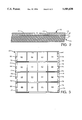
- FIG. 3 is a top view of the x-ray detector for the automatic exposure controller.
- an x-ray imaging system 14 includes an x-ray tube 15 which emits an x-ray beam 17 when excited by power supply 16. As illustrated, the x-ray beam 17 is directed through a patient 18 lying on an x-ray transmissive table 20 and impinge upon a detector assembly designated 22.
- the detector assembly 22 comprises an automatic exposure control (AEC) detector 23 and an imaging device 25 formed in this embodiments by a scintillator 24 in front of a two-dimensional photodetector array 26.
- the scintillator 24 converts the x-ray protons to lower energy photons in the visible spectrum and the photodetector array 26, contiguous with the scintillator, converts the light photons into electrical signals.
- the scintillator 24 and photodetector array 26 are well-known components of conventional x-ray detector assemblies used in previous x-ray imaging systems.
- the AEC detector 23 can be located on the remote side of the detector assembly 22 from the x-ray tube 15.
- the AEC detector 23 may be used with other types of imaging devices 25, such as an image intensifier with a video camera, or even x-ray film.
- a detector controller 27 contains electronics for operating the photodetector array 26 acquire an image by reading a signal from each photodetector element in the two-dimensional array.
- the output signal from the photodetector array 26 is coupled to an image processor 28 that includes circuitry for processing and enhancing the x-ray image signal.
- the processed image then is displayed on a video monitor 32 and may be archived in an image Storage device 30.
- the overall operation of the x-ray imaging system 14 is governed by a system controller 36 which receives commands from the operator via an operator panel 38.
- the x-ray exposure is controlled automatically by a feedback loop that includes the AEC x-ray detector 23 and an exposure control circuit 34.
- the AEC x-ray detector 23 produces a plurality of electrical signals corresponding to the intensity of the x-rays impinging different regions of the detector. Those signals are applied to inputs of the exposure control circuit 34 along with signals from the system controller 36 designating the desired x-ray dose selected by the operator.
- the exposure control circuit 34 responds to these input signals by producing a command signal for the x-ray tube power supply 16 which defines the bias voltage and filament current levels for the x-ray tube 15 to produce the desired x-ray dosage.
- the exposure control 34 responds to the AEC detector signal, which indicates the intensity of the x-rays passing through the patient 18, by commanding the power supply 16 to increase or decrease the bias voltage and filament current for the x-ray tube 15 to achieve an optimal x-ray exposure for a satisfactory image.
- the present invention relates to the unique multiple layer structure of the AEC detector 23 shown in FIG. 2.
- the active layers are formed on a surface of substrate 40 which preferably comprises a low density carbon composite material containing fibers in a matrix material.
- substrate 40 which preferably comprises a low density carbon composite material containing fibers in a matrix material.
- Use of such conventional carbon composites is particularly desirable when the AEC detector 23 is placed in front of the photodetector array 26, as the low density material is x-ray transmissive and provides uniform x-ray attenuation.
- the carbon composite does not induce artifacts in the signal produced by photodetector array 26 enabling the AEC x-ray detector 23 to be placed in front of the scintillator 24 and photodetector array 26.
- the x-ray transmission characteristics of the substrate 40 are not critical and other materials may be employed.
- a uniform first electrode layer 42 is applied over the entire major surface on one side of substrate 40 and serves as a high voltage bias electrode.
- the first electrode layer 42 is formed by either metallization or other conductive material, such as indium tin oxide, deposited by conventional techniques.
- the first electrode layer 42 is relatively thin so as to minimally attenuate x-rays passing therethrough.
- a thin semiconductive layer 44 such as molecular beam epitaxially deposited CdTe, CdZnTe, amorphous silicon or other semiconductor material, extends over the first electrode layer 42.
- the semiconductive layer 44 has a good response to x-rays, high efficiency in converting x-rays to an electrical signal, uniform x-ray transmission and long term x-ray stability.
- the layer 44 of semiconductive material preferably is homogeneous, i.e. p-n junctions are not formed.
- the semiconductive material acts as a solid state ionization chamber in which charged ions are formed in proportion to the intensity of the x-rays which strike the layer. By collecting the ions to form an electrical signal the x-ray intensity can be measured.
- a second electrode layer 46 comprising a plurality of conductive elements 47 and 48 in a pattern which enables the sensing of x-rays impinging different regions of the semiconductive layer.
- the second electrode layer 46 is relatively thin so as to minimally attenuate x-rays passing therethrough.
- An exemplary pattern of conductive elements 51-66 is shown in FIG. 3. This pattern is a four-by-four matrix of rectangular elements on the surface of semiconductive layer 44.
- Four conductive elements 51, 55, 59, and 63 along one edge 71 of the AEC detector 23 are connected electrically to individual contact pads 68 in a first margin 70 along that edge 71.
- An additional set of four contact pads 72 is formed on the first margin 70 with conductive stripes extending therefrom between the outer electrode elements to interior electrode elements 52, 56, 60 and 64.
- the opposite side 73 of the AEC detector 23 has a second margin 74 with for contact pads 76 connected to outer electrode elements 54, 58, 62 and 66 immediately adjacent the second margin.
- Another set of four contact pads 78 is formed within the second margin 74 with separate conductors extending therefrom between the outer electrode elements to four interior electrode elements 53, 57, 61, and 65.
- the second margin 74 has an additional contact pad 80 which extends through an opening in the semiconductive layer 44 to provide electrical contact with the first electrode layer 42.
- the plurality of contact pads 68, 72, 76, 78 and 80 are connected by individual wires to separate inputs of the exposure control 34.
- the electrode elements do not have to be spaced over the entire surface of the substrate, but may be positioned periodically on the surface or only at the corners depending upon the degree of x-ray sensing desired for the automatic exposure control.
- the semiconductive layer 44 can be configured to operate in any common solid state mode, such as the photovoltaic mode or the photoconductivity mode.
- the exposure control 34 selectively senses the electrical signal produced in the semiconductor material between the first electrode layer 42 and each of the electrode elements 51-66 of the second electrode layer 46. In doing so, the exposure control 34 may apply a high voltage to the first electrode layer 42 to bias the semiconductive layer 44 for drift and collection of x-ray induced charges therein. The collection of charge produces an electrical signal between the first and second electrode layers 42 and 46 which can be locally sensed by detecting the signal at each of the electrode elements 51-66 of the second layer 46.
- the exposure control is able to detect the intensity of x-rays striking different portions of the AEC detector 23 and determine from those various signal samples, the power supply command to produce the desired x-ray dosage for optimal image production.
Landscapes
- Health & Medical Sciences (AREA)
- Life Sciences & Earth Sciences (AREA)
- Spectroscopy & Molecular Physics (AREA)
- Molecular Biology (AREA)
- High Energy & Nuclear Physics (AREA)
- General Physics & Mathematics (AREA)
- Physics & Mathematics (AREA)
- General Health & Medical Sciences (AREA)
- Toxicology (AREA)
- Engineering & Computer Science (AREA)
- Signal Processing (AREA)
- Multimedia (AREA)
- Measurement Of Radiation (AREA)
- Apparatus For Radiation Diagnosis (AREA)
- Solid State Image Pick-Up Elements (AREA)
- Transforming Light Signals Into Electric Signals (AREA)
- Light Receiving Elements (AREA)
Abstract
An x-ray detector for an automatic exposure control system has a substrate of carbon composite material with a first layer of conductive material on a major surface of the substrate. A second layer of homogeneous semiconductive material, such as CdTe, CdZnTe or amorphous silicon, is deposited on the first layer and has an electrical characteristic, such as conductivity, that varies in response to impingement of x-rays. A third layer of conductive material is formed on the surface of the semiconductor layer and is divided into a plurality of electrode elements which define a plurality of regions in the layer of semiconductive material. By sensing the conductivity between the first layer and each of the electrode elements, the intensity of x-rays striking the different regions can be measured.
Description
The present invention relates to automatic exposure control systems for x-ray imaging apparatus; and more particularly to x-ray detectors utilized in such exposure control systems.
Conventional fluoroscopic x-ray imaging equipment include a source for projecting a beam of x-rays through an object being imaged, such as a medical patient. The portion of the beam which passes through the patient impinges upon an x-ray detector which converts the x-rays attenuated by the patient into photons which then are converted into an electric image signal. The x-ray detector may comprise an image intensifier tube and a video camera, or a combination of a scintillator in front of a two-dimensional photodetector array. The electrical image signal from either type of detector is processed to display an image of the patient on a video monitor.
The image signal also is applied to the input of a feedback loop which responds to the level of the image signal by producing a control signal which regulates the x-ray exposure and thus brightness of the image on the video monitor. An example of this type of feedback control is described in U.S. Pat. No. 4,573,183. The control signal regulates the biasing of the x-ray tube and the gain of the video camera. This feedback control loop ensures that the image produced in the video monitor has sufficient brightness and contrast for proper viewing by an x-ray technician or physician.
A general object of the present invention is to provide a separate x-ray detector for the automatic exposure control which is not part of the image detector utilized to produce the image displayed on the video monitor.
Another object of the present invention is to provide an x-ray detector which can be placed in front of or behind the image detector with respect to the source of x-rays.
A further object of the present invention is to provide such a detector which has minimal x-ray attenuation variations so as to minimize inducing visible image artifacts.
These and other objects are fulfilled by an x-ray detector for an automatic exposure control system that comprises a substrate having a major surface on which a first electrode layer is formed. A layer of semiconductive material is deposited on the first electrode and has an electrical characteristic which varies in response to impingement of x-rays. In the preferred embodiment, this latter layer comprises homogeneous semiconductive material, such as CdTe, CdZnTe or amorphous silicon. A second electrode layer is formed on the layer of semiconductor material remote from the first electrode layer. One of the first and second electrode layers is divided into a plurality of conductive elements thereby defining a plurality of regions in the layer of semiconductive material adjacent to each of the plurality of conductive elements.
The semiconductive layer acts as a solid state ion chamber and can be operated in a photovoltaic mode in which an electrical current is produced in this layer in response to x-ray bombardment or operated in a photoconductivity mode in which the conductivity of the semiconductive layer is altered by the x-rays. In either mode, the intensity of x-rays striking the various regions can be measured by sensing the electric current flow between each of the conductive elements and the other electrode layer.
FIG. 1 is a block diagram of an x-ray fluoroscopy system utilizing the present invention;
FIG. 2 is a cross-section view through the x-ray detector for automatic exposure controller shown in FIG. 1; and
FIG. 3 is a top view of the x-ray detector for the automatic exposure controller.
With initial reference to FIG. 1, an x-ray imaging system 14 includes an x-ray tube 15 which emits an x-ray beam 17 when excited by power supply 16. As illustrated, the x-ray beam 17 is directed through a patient 18 lying on an x-ray transmissive table 20 and impinge upon a detector assembly designated 22. The detector assembly 22 comprises an automatic exposure control (AEC) detector 23 and an imaging device 25 formed in this embodiments by a scintillator 24 in front of a two-dimensional photodetector array 26. The scintillator 24 converts the x-ray protons to lower energy photons in the visible spectrum and the photodetector array 26, contiguous with the scintillator, converts the light photons into electrical signals. The scintillator 24 and photodetector array 26 are well-known components of conventional x-ray detector assemblies used in previous x-ray imaging systems. Alternatively, the AEC detector 23 can be located on the remote side of the detector assembly 22 from the x-ray tube 15. The AEC detector 23 may be used with other types of imaging devices 25, such as an image intensifier with a video camera, or even x-ray film.
A detector controller 27 contains electronics for operating the photodetector array 26 acquire an image by reading a signal from each photodetector element in the two-dimensional array. The output signal from the photodetector array 26 is coupled to an image processor 28 that includes circuitry for processing and enhancing the x-ray image signal. The processed image then is displayed on a video monitor 32 and may be archived in an image Storage device 30.
The overall operation of the x-ray imaging system 14 is governed by a system controller 36 which receives commands from the operator via an operator panel 38.
The x-ray exposure is controlled automatically by a feedback loop that includes the AEC x-ray detector 23 and an exposure control circuit 34. The AEC x-ray detector 23 produces a plurality of electrical signals corresponding to the intensity of the x-rays impinging different regions of the detector. Those signals are applied to inputs of the exposure control circuit 34 along with signals from the system controller 36 designating the desired x-ray dose selected by the operator. The exposure control circuit 34 responds to these input signals by producing a command signal for the x-ray tube power supply 16 which defines the bias voltage and filament current levels for the x-ray tube 15 to produce the desired x-ray dosage. During the x-ray exposure, the exposure control 34 responds to the AEC detector signal, which indicates the intensity of the x-rays passing through the patient 18, by commanding the power supply 16 to increase or decrease the bias voltage and filament current for the x-ray tube 15 to achieve an optimal x-ray exposure for a satisfactory image.
The present invention relates to the unique multiple layer structure of the AEC detector 23 shown in FIG. 2. The active layers are formed on a surface of substrate 40 which preferably comprises a low density carbon composite material containing fibers in a matrix material. Use of such conventional carbon composites is particularly desirable when the AEC detector 23 is placed in front of the photodetector array 26, as the low density material is x-ray transmissive and provides uniform x-ray attenuation. As a consequence, the carbon composite does not induce artifacts in the signal produced by photodetector array 26 enabling the AEC x-ray detector 23 to be placed in front of the scintillator 24 and photodetector array 26. When the AEC detector 23 is placed on the remote side of photodetector array 26, the x-ray transmission characteristics of the substrate 40 are not critical and other materials may be employed.
A uniform first electrode layer 42 is applied over the entire major surface on one side of substrate 40 and serves as a high voltage bias electrode. The first electrode layer 42 is formed by either metallization or other conductive material, such as indium tin oxide, deposited by conventional techniques. The first electrode layer 42 is relatively thin so as to minimally attenuate x-rays passing therethrough.
A thin semiconductive layer 44, such as molecular beam epitaxially deposited CdTe, CdZnTe, amorphous silicon or other semiconductor material, extends over the first electrode layer 42. The semiconductive layer 44 has a good response to x-rays, high efficiency in converting x-rays to an electrical signal, uniform x-ray transmission and long term x-ray stability. The layer 44 of semiconductive material preferably is homogeneous, i.e. p-n junctions are not formed. Thus the semiconductive material acts as a solid state ionization chamber in which charged ions are formed in proportion to the intensity of the x-rays which strike the layer. By collecting the ions to form an electrical signal the x-ray intensity can be measured.
On top of the semiconductive layer 44 is a second electrode layer 46 comprising a plurality of conductive elements 47 and 48 in a pattern which enables the sensing of x-rays impinging different regions of the semiconductive layer. The second electrode layer 46 is relatively thin so as to minimally attenuate x-rays passing therethrough. An exemplary pattern of conductive elements 51-66 is shown in FIG. 3. This pattern is a four-by-four matrix of rectangular elements on the surface of semiconductive layer 44. Four conductive elements 51, 55, 59, and 63 along one edge 71 of the AEC detector 23 are connected electrically to individual contact pads 68 in a first margin 70 along that edge 71. An additional set of four contact pads 72 is formed on the first margin 70 with conductive stripes extending therefrom between the outer electrode elements to interior electrode elements 52, 56, 60 and 64. The opposite side 73 of the AEC detector 23 has a second margin 74 with for contact pads 76 connected to outer electrode elements 54, 58, 62 and 66 immediately adjacent the second margin. Another set of four contact pads 78 is formed within the second margin 74 with separate conductors extending therefrom between the outer electrode elements to four interior electrode elements 53, 57, 61, and 65. The second margin 74 has an additional contact pad 80 which extends through an opening in the semiconductive layer 44 to provide electrical contact with the first electrode layer 42. The plurality of contact pads 68, 72, 76, 78 and 80 are connected by individual wires to separate inputs of the exposure control 34.
Although a four-by-four matrix of rectangular electrode elements is illustrated in FIG. 3 other geometric matrix patterns and shapes of individual electrode elements of the second electrode layer 46 are within the purview of the present invention. In addition, the electrode elements do not have to be spaced over the entire surface of the substrate, but may be positioned periodically on the surface or only at the corners depending upon the degree of x-ray sensing desired for the automatic exposure control.
The semiconductive layer 44 can be configured to operate in any common solid state mode, such as the photovoltaic mode or the photoconductivity mode. The exposure control 34 selectively senses the electrical signal produced in the semiconductor material between the first electrode layer 42 and each of the electrode elements 51-66 of the second electrode layer 46. In doing so, the exposure control 34 may apply a high voltage to the first electrode layer 42 to bias the semiconductive layer 44 for drift and collection of x-ray induced charges therein. The collection of charge produces an electrical signal between the first and second electrode layers 42 and 46 which can be locally sensed by detecting the signal at each of the electrode elements 51-66 of the second layer 46.
Thus the exposure control is able to detect the intensity of x-rays striking different portions of the AEC detector 23 and determine from those various signal samples, the power supply command to produce the desired x-ray dosage for optimal image production.
The foregoing description is directed primarily to preferred embodiments of the invention. Although some attention was given to various alternatives within the scope of the invention, it is anticipated that skilled artisans will likely realize additional alternatives that are now apparent from the disclosure of those embodiments. Accordingly, the scope of the invention should be determined from the following claims and not limited by the above disclosure.
Claims (16)
1. An x-ray detector for a medical imaging system, the x-ray detector comprising:
a converter for converting x-rays into visible light;
an imager for converting the visible light received from said converter into an electrical image signal; and
an automatic exposure control x-ray detector adjacent one of the converter and the imager, and including:
a) a substrate having a major surface;
b) a first electrode layer on the major surface;
c) a layer of semiconductive material deposited on the first electrode and having an electrical characteristic that varies in response to impingement of x-rays; and
d) a second electrode layer on the layer of semiconductor material and remote from the first electrode layer;
wherein one of the first and second electrode layers is divided into a plurality of conductive elements thereby defining a plurality of regions in the layer of semiconductive material with each region being adjacent to one of the plurality of conductive elements.
2. The x-ray detector as recited in claim 1 wherein the automatic exposure control x-ray detector is adjacent to the converter; and the substrate is a carbon composite material.
3. The x-ray detector as recited in claim 1 wherein the plurality of conductive elements are arranged in an X by Y matrix, where X and Y are positive integers.
4. The x-ray detector as recited in claim 1 wherein the layer of semiconductive material is homogeneous.
5. The x-ray detector as recited in claim 1 wherein the semiconductive material is selected from a group consisting of CdTe, CdZnTe and amorphous silicon.
6. An detector assembly for an x-ray imaging system which has a source of x-rays, the detector assembly comprising:
a two-dimensional photodetector array which produces a signal from which the x-ray imaging system produces an image; and
an detector array for an automatic exposure control of the x-ray imaging system, wherein the detector array is adjacent to the two-dimensional photodetector array and comprises:
(a) a substrate having a major surface;
(b) a first electrode layer on the major surface;
(c) a layer of semiconductive material deposited on the first electrode, and having an electrical characteristic that varies in response to impingement of X-rays; and
(d) a second electrode layer on the layer of semiconductor material and remote from the first electrode layer;
wherein one of the first and second electrode layers is divided into a plurality of conductive elements thereby defining a plurality of regions in the layer of semiconductive material with each region being adjacent to one of the plurality of conductive elements.
7. The detector assembly as recited in claim 6 wherein the two-dimensional photodetector array has a major surface that faces a major surface of the detector array.
8. The detector assembly as recited in claim 6 wherein the two-dimensional photodetector array has a major surface that abuts a major surface of the detector array.
9. The detector assembly as recited in claim 6 wherein the plurality of conductive elements are arranged in an X by Y matrix, where X and Y are positive integers.
10. The detector assembly as recited in claim 6 wherein the substrate is a carbon composite material.
11. The detector assembly as recited in claim 6 wherein the layer of semiconductive material is homogeneous.
12. The detector assembly as recited in claim 6 wherein the semiconductive material is selected from a group consisting of CdTe, CdZnTe and amorphous silicon.
13. The detector assembly as recited in claim 6 further comprising a scintillator between the source of x-rays and both the two-dimensional photodetector array and the detector array.
14. An detector assembly for an x-ray imaging system which has a source of x-rays, the detector assembly comprising:
a two-dimensional photodetector array that produces a signal from which the x-ray imaging system produces an image; and
an detector array for an automatic exposure control of the x-ray imaging system, wherein the detector array is adjacent to the two-dimensional photodetector array and comprises:
(a) a substrate having a major surface;
(b) a first layer of conductive material forming a single electrode on the major surface;
(c) a second layer of semiconductive material deposited on the first electrode and having a surface opposed to the first electrode, the semiconductive material having an electrical characteristic that varies in response to impingement of x-rays; and
(d) a third layer of conductive material on the surface of the layer of semiconductor material, and being divided into a plurality of electrode elements thereby defining a plurality of regions in the layer of semiconductive material with each region being adjacent to one of the plurality of electrode elements.
15. The x-ray detector as recited in claim 14 wherein the layer of semiconductive material is homogeneous.
16. The x-ray detector as recited in claim 14 wherein the semiconductive material is selected from a group consisting of CdTe, CdZnTe and amorphous silicon.
Priority Applications (3)
| Application Number | Priority Date | Filing Date | Title |
|---|---|---|---|
| US08/572,409 US5585638A (en) | 1995-12-14 | 1995-12-14 | X-ray detector for automatic exposure control of an imaging apparatus |
| JP8327398A JPH09257947A (en) | 1995-12-14 | 1996-12-09 | X-ray detector for automatic exposure control system and X-ray detector for medical imaging system |
| EP96308922A EP0779521A1 (en) | 1995-12-14 | 1996-12-10 | X-ray detector for automatic exposure control of an imaging apparatus |
Applications Claiming Priority (1)
| Application Number | Priority Date | Filing Date | Title |
|---|---|---|---|
| US08/572,409 US5585638A (en) | 1995-12-14 | 1995-12-14 | X-ray detector for automatic exposure control of an imaging apparatus |
Publications (1)
| Publication Number | Publication Date |
|---|---|
| US5585638A true US5585638A (en) | 1996-12-17 |
Family
ID=24287684
Family Applications (1)
| Application Number | Title | Priority Date | Filing Date |
|---|---|---|---|
| US08/572,409 Expired - Fee Related US5585638A (en) | 1995-12-14 | 1995-12-14 | X-ray detector for automatic exposure control of an imaging apparatus |
Country Status (3)
| Country | Link |
|---|---|
| US (1) | US5585638A (en) |
| EP (1) | EP0779521A1 (en) |
| JP (1) | JPH09257947A (en) |
Cited By (29)
| Publication number | Priority date | Publication date | Assignee | Title |
|---|---|---|---|---|
| WO1998003884A1 (en) * | 1996-07-19 | 1998-01-29 | Varian Associates, Inc. | X-ray imaging apparatus and method using a flat amorphous silicon imaging panel |
| EP0849980A1 (en) * | 1996-12-20 | 1998-06-24 | General Electric Company | An x-ray imaging system using an image detector |
| EP0929195A3 (en) * | 1998-01-09 | 2000-07-19 | Canon Kabushiki Kaisha | Radiographic image processing apparatus and method |
| US6236051B1 (en) * | 1998-03-27 | 2001-05-22 | Kabushiki Kaisha Toshiba | Semiconductor radiation detector |
| US6285028B1 (en) * | 1998-06-02 | 2001-09-04 | Kabushiki Kaisha Toshiba | Semiconductor radiation detector and nuclear medicine diagnostic apparatus |
| DE10009954A1 (en) * | 2000-03-02 | 2001-09-13 | Siemens Ag | Flat image detector for electromagnetic rays, especially X-rays |
| WO2002006853A1 (en) * | 2000-03-31 | 2002-01-24 | Koninklijke Philips Electronics N.V. | Fdxd-detector for measuring dose |
| US6359967B1 (en) | 1998-11-25 | 2002-03-19 | General Electric Company | Method and apparatus for scan charge compensation in a digital detector |
| US6404851B1 (en) | 2000-03-30 | 2002-06-11 | General Electric Company | Method and apparatus for automatic exposure control using localized capacitive coupling in a matrix-addressed imaging panel |
| WO2002079805A1 (en) * | 2001-03-02 | 2002-10-10 | MAX-PLANCK-Gesellschaft zur Förderung der Wissenschaften e.V. | Device and method for the detection of x-rays |
| US6531225B1 (en) | 1998-06-18 | 2003-03-11 | Hamamatsu Photonics K.K. | Scintillator panel and radiation image sensor |
| US20030161437A1 (en) * | 2002-02-27 | 2003-08-28 | Hoffman David M. | Fiber optic scintillator with optical gain for a computed tomography system and method of manufacturing same |
| US20040002085A1 (en) * | 1999-04-27 | 2004-01-01 | Schembri Carol T. | Apparatus, systems and method for assaying biological materials using an annular format |
| US20040149920A1 (en) * | 2003-01-27 | 2004-08-05 | Takamasa Ishii | Radiographic apparatus and radiographic system |
| EP1446683A1 (en) * | 2001-11-14 | 2004-08-18 | Universite Pierre Et Marie Curie | Radiological imagery method and device |
| US20040179650A1 (en) * | 2003-03-14 | 2004-09-16 | Hoffman David M. | Ct detector array with uniform cross-talk |
| US6873678B2 (en) | 2000-12-28 | 2005-03-29 | Ge Medical Systems Global Technology Company Llc | Methods and apparatus for computed tomographic cardiac or organ imaging |
| US20050151085A1 (en) * | 2004-01-09 | 2005-07-14 | Imascope Inc. | Digital image collector for X-ray systems |
| US20050213706A1 (en) * | 2004-03-29 | 2005-09-29 | Siemens Medical Solutions Usa, Inc. | Medical imaging system with dosimetry for estimating circuit board life |
| US6982425B1 (en) | 1998-06-26 | 2006-01-03 | Ftni Inc. | Indirect x-ray image detector for radiology |
| US7167539B1 (en) | 2002-02-25 | 2007-01-23 | General Electric Company | Thermal sensing detector cell for a computed tomography system and method of manufacturing same |
| US20070165781A1 (en) * | 2004-02-13 | 2007-07-19 | Sectra Mamea Ab | Method and arrangement relating to x-ray imaging |
| US20080232549A1 (en) * | 2005-08-09 | 2008-09-25 | Koninklijke Philips Electronics, N.V. | System and Method For Dual Energy Dynamica X-Ray Imaging |
| US20110103544A1 (en) * | 2009-11-05 | 2011-05-05 | Nathan Hermony | Diagnostic imaging system and method using multiple types of imaging detectors |
| US20110180714A1 (en) * | 2010-01-25 | 2011-07-28 | Fujifilm Corporation | Radiation detector |
| US20150115163A1 (en) * | 2012-04-20 | 2015-04-30 | Sony Corporation | Semiconductor photodetector and radial ray detector |
| CN110192435A (en) * | 2016-12-08 | 2019-08-30 | 维苏斯健康信息技术有限责任公司 | Detector strip for X-ray film |
| WO2020093240A1 (en) * | 2018-11-06 | 2020-05-14 | Shenzhen Xpectvision Technology Co., Ltd. | A radiation detector |
| IT201900001225A1 (en) | 2019-01-28 | 2020-07-28 | General Medical Merate S P A | Predictive method to control a radiological equipment and radiological equipment that implements it |
Families Citing this family (5)
| Publication number | Priority date | Publication date | Assignee | Title |
|---|---|---|---|---|
| JPH11206746A (en) * | 1998-01-30 | 1999-08-03 | Shimadzu Corp | X-ray diagnostic equipment |
| JP3678162B2 (en) * | 2001-04-12 | 2005-08-03 | 株式会社島津製作所 | Radiation detector |
| US6953935B1 (en) * | 2004-05-11 | 2005-10-11 | General Electric Company | CT detector fabrication process |
| JP5683856B2 (en) * | 2010-07-15 | 2015-03-11 | 日立アロカメディカル株式会社 | Radiation detector |
| WO2012014538A1 (en) * | 2010-07-26 | 2012-02-02 | 富士フイルム株式会社 | Radiation detector panel |
Citations (6)
| Publication number | Priority date | Publication date | Assignee | Title |
|---|---|---|---|---|
| US4996413A (en) * | 1990-02-27 | 1991-02-26 | General Electric Company | Apparatus and method for reading data from an image detector |
| US5012504A (en) * | 1989-12-26 | 1991-04-30 | General Electric Company | Automatic brightness compensation for fluorography systems |
| US5079426A (en) * | 1989-09-06 | 1992-01-07 | The Regents Of The University Of Michigan | Multi-element-amorphous-silicon-detector-array for real-time imaging and dosimetry of megavoltage photons and diagnostic X rays |
| US5194736A (en) * | 1990-11-14 | 1993-03-16 | U.S. Philips Corp. | X-ray examination apparatus including a matrix of sensors and device measuring exposure of groups of sensors during execution of an x-ray exposure |
| US5254480A (en) * | 1992-02-20 | 1993-10-19 | Minnesota Mining And Manufacturing Company | Process for producing a large area solid state radiation detector |
| US5264701A (en) * | 1992-03-26 | 1993-11-23 | General Electric Company | Ion chamber for X-ray detection |
Family Cites Families (8)
| Publication number | Priority date | Publication date | Assignee | Title |
|---|---|---|---|---|
| JPS56119876A (en) * | 1980-02-27 | 1981-09-19 | Toshiba Corp | Semiconductor x-ray detector |
| US4573183A (en) | 1984-06-29 | 1986-02-25 | General Electric Company | X-Ray image brightness control |
| JPS6243585A (en) * | 1985-08-21 | 1987-02-25 | Toshiba Corp | Detector for x ray ct |
| US4926052A (en) * | 1986-03-03 | 1990-05-15 | Kabushiki Kaisha Toshiba | Radiation detecting device |
| DE9107256U1 (en) * | 1991-06-12 | 1991-08-08 | Siemens AG, 80333 München | X-ray exposure machine |
| JPH07500454A (en) * | 1991-07-31 | 1995-01-12 | ザ リージェンツ オブ ザ ユニバーシティ オブ カリフォルニア | Improving the spatial resolution of particle detectors |
| DE4125928A1 (en) * | 1991-08-05 | 1993-02-11 | Siemens Ag | DETECTOR SYSTEM |
| US5693947A (en) * | 1993-04-28 | 1997-12-02 | The University Of Surrey | Radiation detectors |
-
1995
- 1995-12-14 US US08/572,409 patent/US5585638A/en not_active Expired - Fee Related
-
1996
- 1996-12-09 JP JP8327398A patent/JPH09257947A/en not_active Withdrawn
- 1996-12-10 EP EP96308922A patent/EP0779521A1/en not_active Withdrawn
Patent Citations (6)
| Publication number | Priority date | Publication date | Assignee | Title |
|---|---|---|---|---|
| US5079426A (en) * | 1989-09-06 | 1992-01-07 | The Regents Of The University Of Michigan | Multi-element-amorphous-silicon-detector-array for real-time imaging and dosimetry of megavoltage photons and diagnostic X rays |
| US5012504A (en) * | 1989-12-26 | 1991-04-30 | General Electric Company | Automatic brightness compensation for fluorography systems |
| US4996413A (en) * | 1990-02-27 | 1991-02-26 | General Electric Company | Apparatus and method for reading data from an image detector |
| US5194736A (en) * | 1990-11-14 | 1993-03-16 | U.S. Philips Corp. | X-ray examination apparatus including a matrix of sensors and device measuring exposure of groups of sensors during execution of an x-ray exposure |
| US5254480A (en) * | 1992-02-20 | 1993-10-19 | Minnesota Mining And Manufacturing Company | Process for producing a large area solid state radiation detector |
| US5264701A (en) * | 1992-03-26 | 1993-11-23 | General Electric Company | Ion chamber for X-ray detection |
Cited By (50)
| Publication number | Priority date | Publication date | Assignee | Title |
|---|---|---|---|---|
| US5949848A (en) * | 1996-07-19 | 1999-09-07 | Varian Assocaites, Inc. | X-ray imaging apparatus and method using a flat amorphous silicon imaging panel |
| WO1998003884A1 (en) * | 1996-07-19 | 1998-01-29 | Varian Associates, Inc. | X-ray imaging apparatus and method using a flat amorphous silicon imaging panel |
| EP0849980A1 (en) * | 1996-12-20 | 1998-06-24 | General Electric Company | An x-ray imaging system using an image detector |
| EP0929195A3 (en) * | 1998-01-09 | 2000-07-19 | Canon Kabushiki Kaisha | Radiographic image processing apparatus and method |
| US6731783B2 (en) * | 1998-01-09 | 2004-05-04 | Canon Kabushiki Kaisha | Image processing apparatus and method |
| US6236051B1 (en) * | 1998-03-27 | 2001-05-22 | Kabushiki Kaisha Toshiba | Semiconductor radiation detector |
| US6285028B1 (en) * | 1998-06-02 | 2001-09-04 | Kabushiki Kaisha Toshiba | Semiconductor radiation detector and nuclear medicine diagnostic apparatus |
| US6531225B1 (en) | 1998-06-18 | 2003-03-11 | Hamamatsu Photonics K.K. | Scintillator panel and radiation image sensor |
| US7112801B2 (en) | 1998-06-18 | 2006-09-26 | Hamamatsu Photonics K.K. | Scintillator panel and radiation image sensor |
| US6849336B2 (en) | 1998-06-18 | 2005-02-01 | Hamamatsu Photonics K.K. | Scintillator panel and radiation image sensor |
| EP1156346A3 (en) * | 1998-06-18 | 2003-12-03 | Hamamatsu Photonics K.K. | Scintillator panel and radiation image sensor |
| US20060027760A1 (en) * | 1998-06-26 | 2006-02-09 | Rougeot Henri M | Indirect x-ray image detector for radiology |
| US7692157B2 (en) | 1998-06-26 | 2010-04-06 | Ftni Inc. | Indirect x-ray image detector for radiology |
| US6982425B1 (en) | 1998-06-26 | 2006-01-03 | Ftni Inc. | Indirect x-ray image detector for radiology |
| US6359967B1 (en) | 1998-11-25 | 2002-03-19 | General Electric Company | Method and apparatus for scan charge compensation in a digital detector |
| US20040002085A1 (en) * | 1999-04-27 | 2004-01-01 | Schembri Carol T. | Apparatus, systems and method for assaying biological materials using an annular format |
| DE10009954A1 (en) * | 2000-03-02 | 2001-09-13 | Siemens Ag | Flat image detector for electromagnetic rays, especially X-rays |
| US6404851B1 (en) | 2000-03-30 | 2002-06-11 | General Electric Company | Method and apparatus for automatic exposure control using localized capacitive coupling in a matrix-addressed imaging panel |
| WO2002006853A1 (en) * | 2000-03-31 | 2002-01-24 | Koninklijke Philips Electronics N.V. | Fdxd-detector for measuring dose |
| US6873678B2 (en) | 2000-12-28 | 2005-03-29 | Ge Medical Systems Global Technology Company Llc | Methods and apparatus for computed tomographic cardiac or organ imaging |
| WO2002079805A1 (en) * | 2001-03-02 | 2002-10-10 | MAX-PLANCK-Gesellschaft zur Förderung der Wissenschaften e.V. | Device and method for the detection of x-rays |
| EP1446683A1 (en) * | 2001-11-14 | 2004-08-18 | Universite Pierre Et Marie Curie | Radiological imagery method and device |
| US7167539B1 (en) | 2002-02-25 | 2007-01-23 | General Electric Company | Thermal sensing detector cell for a computed tomography system and method of manufacturing same |
| US20030161437A1 (en) * | 2002-02-27 | 2003-08-28 | Hoffman David M. | Fiber optic scintillator with optical gain for a computed tomography system and method of manufacturing same |
| US7078701B2 (en) | 2003-01-27 | 2006-07-18 | Canon Kabushiki Kaisha | Radiographic apparatus and radiographic system |
| US20040149920A1 (en) * | 2003-01-27 | 2004-08-05 | Takamasa Ishii | Radiographic apparatus and radiographic system |
| US6859514B2 (en) | 2003-03-14 | 2005-02-22 | Ge Medical Systems Global Technology Company Llc | CT detector array with uniform cross-talk |
| US20040179650A1 (en) * | 2003-03-14 | 2004-09-16 | Hoffman David M. | Ct detector array with uniform cross-talk |
| US20050151085A1 (en) * | 2004-01-09 | 2005-07-14 | Imascope Inc. | Digital image collector for X-ray systems |
| US7496176B2 (en) | 2004-02-13 | 2009-02-24 | Sectra Mamea | Method and arrangement relating to x-ray imaging |
| US20070165781A1 (en) * | 2004-02-13 | 2007-07-19 | Sectra Mamea Ab | Method and arrangement relating to x-ray imaging |
| DE112005000280B4 (en) * | 2004-02-13 | 2021-03-04 | Philips Digital Mammography Sweden Ab | Method and arrangement relating to image processing by means of X-rays |
| US20050213706A1 (en) * | 2004-03-29 | 2005-09-29 | Siemens Medical Solutions Usa, Inc. | Medical imaging system with dosimetry for estimating circuit board life |
| US7372942B2 (en) * | 2004-03-29 | 2008-05-13 | Siemens Medical Solutions Usa, Inc. | Medical imaging system with dosimetry for estimating circuit board life |
| US20070237297A1 (en) * | 2004-12-01 | 2007-10-11 | Imascope Inc. | Auto exposure measurement system for an x-ray digital image capturer |
| US7289601B2 (en) | 2004-12-01 | 2007-10-30 | Imascope Inc. | Digital image collector for X-ray systems |
| US20080232549A1 (en) * | 2005-08-09 | 2008-09-25 | Koninklijke Philips Electronics, N.V. | System and Method For Dual Energy Dynamica X-Ray Imaging |
| US20110103544A1 (en) * | 2009-11-05 | 2011-05-05 | Nathan Hermony | Diagnostic imaging system and method using multiple types of imaging detectors |
| US9173618B2 (en) * | 2009-11-05 | 2015-11-03 | General Electric Company | Diagnostic imaging system and method using multiple types of imaging detectors |
| US20110180714A1 (en) * | 2010-01-25 | 2011-07-28 | Fujifilm Corporation | Radiation detector |
| US8981304B2 (en) * | 2010-01-25 | 2015-03-17 | Fujifilm Corporation | Radiation detector |
| US9568618B2 (en) * | 2012-04-20 | 2017-02-14 | Sony Semiconductor Solutions Corporation | Semiconductor photodetector and radial ray detector |
| US20150115163A1 (en) * | 2012-04-20 | 2015-04-30 | Sony Corporation | Semiconductor photodetector and radial ray detector |
| CN110192435A (en) * | 2016-12-08 | 2019-08-30 | 维苏斯健康信息技术有限责任公司 | Detector strip for X-ray film |
| US20190302277A1 (en) * | 2016-12-08 | 2019-10-03 | Visus Health It Gmbh | Detector strip for radiographic film |
| US11086027B2 (en) * | 2016-12-08 | 2021-08-10 | Visus Health It Gmbh | Detector strip for x-ray film |
| CN110192435B (en) * | 2016-12-08 | 2023-05-30 | 维苏斯健康信息技术有限责任公司 | Detector band for X-ray film |
| WO2020093240A1 (en) * | 2018-11-06 | 2020-05-14 | Shenzhen Xpectvision Technology Co., Ltd. | A radiation detector |
| US11156730B2 (en) | 2018-11-06 | 2021-10-26 | Shenzhen Xpectvision Technology Co., Ltd. | Radiation detector |
| IT201900001225A1 (en) | 2019-01-28 | 2020-07-28 | General Medical Merate S P A | Predictive method to control a radiological equipment and radiological equipment that implements it |
Also Published As
| Publication number | Publication date |
|---|---|
| EP0779521A1 (en) | 1997-06-18 |
| JPH09257947A (en) | 1997-10-03 |
Similar Documents
| Publication | Publication Date | Title |
|---|---|---|
| US5585638A (en) | X-ray detector for automatic exposure control of an imaging apparatus | |
| EP0849980B1 (en) | An x-ray imaging system using an image detector | |
| Kasap et al. | Direct-conversion flat-panel X-ray image sensors for digital radiography | |
| US5079426A (en) | Multi-element-amorphous-silicon-detector-array for real-time imaging and dosimetry of megavoltage photons and diagnostic X rays | |
| US5962856A (en) | Active matrix X-ray imaging array | |
| KR100289481B1 (en) | Photoelectric conversion device and its driving method | |
| JP4533010B2 (en) | Radiation imaging apparatus, radiation imaging method, and radiation imaging system | |
| CA2127453C (en) | Thin-film, flat panel, pixelated detector array for real-time digital imaging and dosimetry of ionizing radiation | |
| US6316773B1 (en) | Multi-density and multi-atomic number detector media with gas electron multiplier for imaging applications | |
| AU717495B2 (en) | X-ray imaging apparatus and method using a flat amorphous silicon imaging panel | |
| US7514692B2 (en) | Method and apparatus for reducing polarization within an imaging device | |
| EP2144271B1 (en) | X-ray imaging device and x-ray radiographic apparatus | |
| CN102401906A (en) | Radiation detector and its imaging device, electrode structure and method for acquiring images | |
| JP2003194950A (en) | Hybrid detector for X-ray imaging | |
| US3890506A (en) | Fast response time image tube camera | |
| US5574765A (en) | X-Ray Diagnostics installation having a solid-state converter | |
| US20010028701A1 (en) | X-ray diagnostic installation having an X-ray image converter with combined back light/dose measuring unit | |
| EP0035182A2 (en) | Semiconductor radiation sensor arrangement for an automatic X-ray exposure control apparatus | |
| US6359965B1 (en) | Diagnostic radiography system with a flat x-ray image converter with back-illumination | |
| US6795527B2 (en) | Apparatus and method for detection of radiation | |
| US20010019600A1 (en) | Planar image detector for electromagnetic rays, particularly X-rays | |
| Roehrig et al. | Real-time imaging detectors for portal imaging | |
| US6794672B2 (en) | System for the registration of radiation images | |
| CA2218059A1 (en) | Active matrix x-ray imaging array | |
| JP2004154274A (en) | Multiple radiation source x-ray ct apparatus |
Legal Events
| Date | Code | Title | Description |
|---|---|---|---|
| FEPP | Fee payment procedure |
Free format text: PAYOR NUMBER ASSIGNED (ORIGINAL EVENT CODE: ASPN); ENTITY STATUS OF PATENT OWNER: LARGE ENTITY |
|
| FPAY | Fee payment |
Year of fee payment: 4 |
|
| FEPP | Fee payment procedure |
Free format text: PAYER NUMBER DE-ASSIGNED (ORIGINAL EVENT CODE: RMPN); ENTITY STATUS OF PATENT OWNER: LARGE ENTITY Free format text: PAYOR NUMBER ASSIGNED (ORIGINAL EVENT CODE: ASPN); ENTITY STATUS OF PATENT OWNER: LARGE ENTITY |
|
| REMI | Maintenance fee reminder mailed | ||
| LAPS | Lapse for failure to pay maintenance fees | ||
| STCH | Information on status: patent discontinuation |
Free format text: PATENT EXPIRED DUE TO NONPAYMENT OF MAINTENANCE FEES UNDER 37 CFR 1.362 |
|
| FP | Lapsed due to failure to pay maintenance fee |
Effective date: 20041217 |