EP0963686B1 - Organic electroluminescent device - Google Patents
Organic electroluminescent device Download PDFInfo
- Publication number
- EP0963686B1 EP0963686B1 EP98937700A EP98937700A EP0963686B1 EP 0963686 B1 EP0963686 B1 EP 0963686B1 EP 98937700 A EP98937700 A EP 98937700A EP 98937700 A EP98937700 A EP 98937700A EP 0963686 B1 EP0963686 B1 EP 0963686B1
- Authority
- EP
- European Patent Office
- Prior art keywords
- light
- pattern
- electrode
- electroluminescent device
- emitting surface
- Prior art date
- Legal status (The legal status is an assumption and is not a legal conclusion. Google has not performed a legal analysis and makes no representation as to the accuracy of the status listed.)
- Expired - Lifetime
Links
Images


Classifications
-
- H—ELECTRICITY
- H05—ELECTRIC TECHNIQUES NOT OTHERWISE PROVIDED FOR
- H05B—ELECTRIC HEATING; ELECTRIC LIGHT SOURCES NOT OTHERWISE PROVIDED FOR; CIRCUIT ARRANGEMENTS FOR ELECTRIC LIGHT SOURCES, IN GENERAL
- H05B33/00—Electroluminescent light sources
- H05B33/12—Light sources with substantially two-dimensional radiating surfaces
- H05B33/26—Light sources with substantially two-dimensional radiating surfaces characterised by the composition or arrangement of the conductive material used as an electrode
-
- H—ELECTRICITY
- H05—ELECTRIC TECHNIQUES NOT OTHERWISE PROVIDED FOR
- H05B—ELECTRIC HEATING; ELECTRIC LIGHT SOURCES NOT OTHERWISE PROVIDED FOR; CIRCUIT ARRANGEMENTS FOR ELECTRIC LIGHT SOURCES, IN GENERAL
- H05B33/00—Electroluminescent light sources
- H05B33/12—Light sources with substantially two-dimensional radiating surfaces
- H05B33/14—Light sources with substantially two-dimensional radiating surfaces characterised by the chemical or physical composition or the arrangement of the electroluminescent material, or by the simultaneous addition of the electroluminescent material in or onto the light source
-
- H—ELECTRICITY
- H05—ELECTRIC TECHNIQUES NOT OTHERWISE PROVIDED FOR
- H05B—ELECTRIC HEATING; ELECTRIC LIGHT SOURCES NOT OTHERWISE PROVIDED FOR; CIRCUIT ARRANGEMENTS FOR ELECTRIC LIGHT SOURCES, IN GENERAL
- H05B33/00—Electroluminescent light sources
- H05B33/12—Light sources with substantially two-dimensional radiating surfaces
- H05B33/22—Light sources with substantially two-dimensional radiating surfaces characterised by the chemical or physical composition or the arrangement of auxiliary dielectric or reflective layers
-
- H—ELECTRICITY
- H10—SEMICONDUCTOR DEVICES; ELECTRIC SOLID-STATE DEVICES NOT OTHERWISE PROVIDED FOR
- H10K—ORGANIC ELECTRIC SOLID-STATE DEVICES
- H10K50/00—Organic light-emitting devices
- H10K50/80—Constructional details
- H10K50/805—Electrodes
- H10K50/81—Anodes
- H10K50/813—Anodes characterised by their shape
-
- H—ELECTRICITY
- H10—SEMICONDUCTOR DEVICES; ELECTRIC SOLID-STATE DEVICES NOT OTHERWISE PROVIDED FOR
- H10K—ORGANIC ELECTRIC SOLID-STATE DEVICES
- H10K59/00—Integrated devices, or assemblies of multiple devices, comprising at least one organic light-emitting element covered by group H10K50/00
- H10K59/10—OLED displays
- H10K59/221—Static displays, e.g. displaying permanent logos
-
- H—ELECTRICITY
- H10—SEMICONDUCTOR DEVICES; ELECTRIC SOLID-STATE DEVICES NOT OTHERWISE PROVIDED FOR
- H10K—ORGANIC ELECTRIC SOLID-STATE DEVICES
- H10K50/00—Organic light-emitting devices
- H10K50/80—Constructional details
- H10K50/85—Arrangements for extracting light from the devices
- H10K50/854—Arrangements for extracting light from the devices comprising scattering means
-
- H—ELECTRICITY
- H10—SEMICONDUCTOR DEVICES; ELECTRIC SOLID-STATE DEVICES NOT OTHERWISE PROVIDED FOR
- H10K—ORGANIC ELECTRIC SOLID-STATE DEVICES
- H10K59/00—Integrated devices, or assemblies of multiple devices, comprising at least one organic light-emitting element covered by group H10K50/00
- H10K59/10—OLED displays
-
- H—ELECTRICITY
- H10—SEMICONDUCTOR DEVICES; ELECTRIC SOLID-STATE DEVICES NOT OTHERWISE PROVIDED FOR
- H10K—ORGANIC ELECTRIC SOLID-STATE DEVICES
- H10K59/00—Integrated devices, or assemblies of multiple devices, comprising at least one organic light-emitting element covered by group H10K50/00
- H10K59/30—Devices specially adapted for multicolour light emission
- H10K59/38—Devices specially adapted for multicolour light emission comprising colour filters or colour changing media [CCM]
Definitions
- the invention relates to an electroluminescent device exhibiting a pattern-wise light-emitting surface when driven, said electroluminescent device comprising an organic emitter layer having an electroluminescent area, a first electrode layer and a second electrode layer, said organic emitter layer being disposed between said first and said second electrode layer.
- the known EL device is an EL device in which the electroluminescence originates from an organic compound, or an organic EL device for short.
- the known organic EL device comprises a polyphenylenevinylene emitter layer disposed between an indium tin oxide (ITO) and an indium electrode layer.
- the organic emitter layer comprises electroluminescent areas in accordance with a desired pattern. When driven, the surface of the EL device emits light in accordance with said desired pattern.
- the electrode layers may be structured according to the desired pattern.
- the EL device disclosed in International Patent Application WO 97/06223 is particularly suitable to display icons.
- An icon is a specific high-resolution image having a fixed shape and color (scheme) which can be switched (partially) on or off. It may take the form of a pictogram, a word like "STOP" or "GO", or a number. Alternatively, it may be an area having a color which is different from the color of the area surrounding it. Icons are a clear and attractive means to convey information and are abundantly used in, for example, segmented display devices where they provide information complementary to the information provided by the segmented display area of the display device.
- a disadvantage of the known EL device is that if a group of icons is to be accommodated, a relatively large display area will be required. This is of particular concern in portable applications, such as the display panel of a mobile phone, where display area is at a premium. Also, from the viewpoint of design and/or ergonomy it may be less attractive to have a large part of the display area occupied by a group of icons of which many, due to the nature of the information they are to provide, will be off most of the time.
- An object of the invention is. inter alia, to reduce the disadvantages mentioned hereinabove. Specifically, it is an object of the invention to provide an organic EL device capable of displaying a group of icons whilst requiring a modest amount of display area.
- an electroluminescent device as mentioned in the opening paragraph which, in accordance with the invention, is characterized in that the first electrode layer has an electrode area which is split up into a first and a second electrode which are independently driveable and mutually interlaced,
- the first and second electrode must be independently driveable.
- the EL device When driven, that is when supplying a suitable voltage between the first (second) and the common electrode, the EL device will exhibit a first (second) pattern-wise light-emitting surface, and thus the first (second) icon is switched on.
- the first and second icon are spread out across the same part of the display area. If the spacing between various parts of the first (second) electrode is chosen small enough (which can be readily done by using, for example, photolithography), the image associated with the first (second) electrode, as presented to the unaided eye will, although in fact interrupted by the second (first) electrode, appear to be a continuous image.
- interlacing has the same meaning as terms like interlineating, interweaving and interdigitating.
- a mutually interlaced first and second electrode can be obtained by, for example, mutually engaging a first and second comb-shaped electrode or, in particular if more than two electrodes are to be interlaced, by mutually intertwisting flat spiral-shaped electrodes.
- the EL device in accordance with the invention is not only less complicated in terms of construction than a pixelated EL display device, such as a segmented or matrix EL display device, but it also allows, while employing the same patterning method, images of higher resolution to be displayed.
- One of the electrode layers serves as a hole-injecting layer. also referred to as the anode, and the other electrode layer serves as an electron-injecting layer, also referred to as the cathode. At least one of the electrode layers has to be transparent to the light to be emitted.
- the EL device may include charge-injection and charge-transport layers, while EL devices based on EL compounds of low molecular weight preferably include such layers.
- suitable (transparent) hole-injecting and electron-injecting electrodes and emitter layers containing organic compounds of low molar mass include those disclosed in the European Patent Applications EP-A-278757 and EP-A-553950.
- electroluminescent organic compounds of high molecular weight notably electroluminescent polymers such as a polyphenylenevinylene, may be suitably used.
- suitable EL polymers include those disclosed in United States Patent US 5,247,190.
- the cathode is used as the common electrode.
- the common electrode requires less patterning of image-sensitive areas than the first and second electrodes. while cathodic materials are more difficult to pattern due to their high chemical reactivity.
- a preferred embodiment of the EL device in accordance with the invention is characterized in that the electroluminescent device further comprises a light-scattering layer scattering the light emitted by the electroluminescent device. If comb-shaped electrodes are employed, an anisotropically scattering layer may be effectively used which selectively scatters the emitted light in a direction substantially at right angles to the direction of the teeth of the comb-electrodes.
- the common electrode, the first (second) electrode and/or the electroluminescent area can all be patterned so as to manipulate the actually light-emitting surface.
- first and the second light-emitting surface are chosen to be the same, one of them may be advantageously used as a backup for the other, thus improving the service life and/or the reliability of the EL device.
- icons differing in shape are to be selectively displayed using the same part of the display area, use is to be made of a preferred embodiment of the electroluminescent device which is characterized in that the first pattern-wise light-emitting surface is different from the second pattern-wise light-emitting surface.
- This problem can be solved by an embodiment of the EL device in accordance with the invention which is characterized in that the emitter layer comprises electroluminescent areas in accordance with a desired pattern.
- the pattern can simply be chosen such that at those locations where an electric lead is present the emitter layer does not have an electroluminescent area.
- the common electrode need not be patterned at all in order to obtain a pattern-wise light-emitting surface but can simply be chosen so as to cover the entire electrode area of the first electrode layer.
- An example of a suitable patterned emitter layer is disclosed in the International Patent Application WO 97/06223.
- An alternative solution is to employ a structured electrode layer of the type disclosed in International Patent Application WO 96/08047.
- electroluminescent device in accordance with the invention is characterized in that the electroluminescent device comprises a color layer having a light-absorbing pattern which covers the first pattern-wise light-emitting surface and leaves the second pattern-wise light-emitting surface uncovered.
- a group of icons differing in color can be selectively displayed using the same part of a display area even when the emission spectrum of the first and second light-emitting surface is the same.
- different colors may be obtained by driving the electrodes at the same voltage in a pulsed manner, the luminance being controlled by means of the frequency and duration of each pulse.
- the light-absorbing pattern is selectively light-absorbing with respect to the light-emitting surface if the emission spectrum of the light-emitting surface and the absorption spectrum of the light-absorbing pattern of the color layer demonstrate a partial overlap.
- the color layer should not absorb the light at all wavelengths of the emission spectrum, i.e. it is to be selective otherwise the light emitting surface will appear dark.
- the second light-emitting surface may be covered by a similar color layer.
- the first and second light-absorbing patterns may, but preferably do not, absorb the same part of the spectrum of light emitted by the first and second light-emitting surface.
- the first and second light-absorbing patterns may be accommodated by the same layer or separate layers.
- the color layers are in fact color filters and their use leads to loss of emitted light.
- An embodiment of the EL device which is improved in this respect is characterized in that the light-absorbing pattern of the color layer is a photoluminescent pattern.
- the loss of light due to absorption of emitted light in the light-absorbing pattern is reduced if absorbed photons are re-emitted or are transferred to and then re-emitted by a photoluminescent material.
- the photoluminescent material may be present in addition to or may replace the light-absorbing material of the light absorbing pattern. Suitable photoluminescent materials include fluorescent and phosphorescent materials.
- Loss of emitted light due to reflection may be reduced by providing the color layer on the light-emitting surface.
- Electroluminescent polymers in particular polyphenylenevinylenes, emit light within a broad range of wavelengths.
- the emission spectrum may be 200 to 300 nm wide and substantially overlap the visible light spectrum. Such a broad emission spectrum allows a large variety of colors to be displayed using color layers.
- a particularly preferred embodiment of the electroluminescent device in accordance with the invention is characterized in that the light-absorbing pattern is repeated beyond the first pattern-wise light-emitting surface. If the area in which the multi-color icons are to be selectively displayed is only a part of a larger display area, that area will, due to reflection of ambient light from the light-absorbing pattern, display a color different from the rest of the display area even if the EL device is not driven. This undesirable effect may be suppressed by repeating the light-absorbing pattern beyond the light-emitting surface so as to cover the entire display area of the display panel. For example, if use is made of comb-shaped electrodes, the first light-absorbing pattern can be a plurality of stripes running parallel to and covering the teeth of the first comb-shaped electrode.
- the EL device in accordance with the invention may be suitably used as a backlight, in particular as a multi-color backlight, in, for example, a liquid crystal display device.
- the EL device in accordance with the invention may be suitably used as (part of) a display device, such as a segmented or matrix display device or an illuminated advertisement board, or may be suitably complemented so as to form such a display device.
- Fig. 1 is a schematic transparent plan view of a first embodiment of an EL device 1 in accordance with the invention.
- the EL device 1 is a display device having a display area of which only a part 2 is shown.
- the EL device 1 comprises a substrate 8, which in the present embodiment is transparent with respect to the light to be emitted and which is provided with a first electrode layer indicated by the reference sign 3 in Fig. 2.
- the electrode layer 3 has an electrode area coinciding with the area indicated by the reference sign 2 in Fig. 1 which is split up into a first comb-shaped electrode 3A and a second comb-shaped electrode 3B.
- the electrodes 3A and 3B can be independently driven by means of the terminals 4A and 4B.
- the teeth of the combs engage so as to form mutually interlaced electrodes 3A and 3B.
- the electrodes 3A and 3B are transparent with respect to the light to be emitted.
- the electrode layer 3 is covered by the organic emitter layer 5.
- the emitter layer 5 has an electroluminescent area which encompasses the entire emitter layer.
- a second electrode layer which serves as a common electrode 6 having a pattern in the form of a sand glass and which can be driven by means of the terminal 7.
- the EL device 1 can be manufactured as follows:
- a conjugated 2,5-dialkoxy-substituted polyphenylenevinylene poly[2-methoxy-5-(3,7-dimethyloctyloxy)-p-phenylene vinylene] is prepared by polymerization of 1,4-bischloromethyl-2-methoxy-5-(3,7-dimethyloctyloxy)benzene. The preparation is described in an article by D. Braun et al., Synthetic Metals. 66 (1994) pp 75-79. The polymer is readily soluble, inter alia, in toluene, tetrahydrofuran and xylene.
- a transparent indium-tin-oxide (ITO) first electrode layer 3 having a thickness of 150 nm and a surface resistance of less than 20 ⁇ /square is deposited by means of sputtering onto a glass substrate 8.
- Said layer 3 serves as the electrode layer for injecting holes into the emitter layer 5 of conjugated poly[2-methoxy-5-(3,7-dimethyloctyloxy)-1,4-phenylene vinylene] which is to be provided later.
- the ITO is then etched, using a conventional method, in accordance with the pattern shown in Fig. 1 so as to split up the electrode area of the first electrode layer into the first comb-shaped electrode 3A and the second comb-shaped electrode 3B.
- the 100 nm thick organic emitter layer 5 is manufactured by spin coating an 0.6 wt.% solution of the above-mentioned polymer in toluene at a rate of 1000 r.p.m. for 25 s.
- a metal mask in which the sand glass shaped pattern shown in Fig. 1 is cut out is positioned above the emitter layer 5, and by means of vacuum deposition a 150 nm thick layer of Yb in accordance with said pattern is deposited, thereby forming the common electrode 6 which serves as the electron-injecting electrode.
- the EL device 1 is now complete. By supplying a voltage of, for example, 5 V to the terminals 4A and 7, using terminal 4A as the positive terminal, an orange-colored light-emitting icon in the form of a triangle pointing upwards emerges.
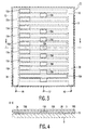
- Fig. 3 is a schematic transparent plan view of a second embodiment of an EL device, indicated by the reference sign 11, in accordance with the invention. It is similar to the first embodiment but differs in that the emitter layer is now a patterned emitter layer, indicated by the reference sign 15 in Fig. 4, and the common electrode 16 is not a patterned electrode, at least not inside the part 12 of the display area.
- the emitter layer 15 is a patchwork-pattern layer having electroluminescent areas 15A and non-electroluminescent areas 15B.
- This second embodiment may be manufactured, for example. by using the method disclosed in the first embodiment, with this difference that before the common electrode 16 is provided, the emitter layer is irradated in accordance with the pattern formed by the areas 15A shown in Fig. 3 and according to a procedure disclosed in International Patent Application WO 97/06223.
- Fig. 5 is a schematic plan view of the electrode arrangement of a third embodiment of an EL device 31 in accordance with the invention.
- the electrode area 32 of the first electrode layer of the EL device 31 is split up into flat spiral-shaped electrodes 33A and 33B which are mutually intertwisted.
- Fig. 6 is a schematic transparent plan view of a fourth embodiment of an EL device 61 in accordance with the invention.
- the EL device 61 shown in Fig. 6 is a backlight but it may also be (part of) a display area of an EL display device.
- the EL device 61 has a first and a second comb-shaped electrode 63A and 63B which are mutually interlaced, and a common electrode 66 which entirely covers the first and second electrode.
- the pattern of the first (second) light-emitting surface corresponds to the pattern of the electrode 63A (63B).
- Fig. 6 further shows that the EL device is provided with a color layer 67 which is located on a light-emitting side of said EL device 61.
- the color layer 67 has a light-absorbing pattern consisting of the stripes 67A which selectively absorbs only a selected range of wavelengths of the light emitted.
- the stripes 67A cover the teeth of the electrode 63A.
- the teeth of the second electrode 63B are left uncovered.
- the light-absorbing pattern 67A is a pattern which is repeated beyond the teeth of the electrode 63A and is present on the entire surface area of the backlight.
- the stripes 67B together constitute a pattern which is transparent to the light to be emitted.
- the pattern 67B may be a light-absorbing pattern to be accommodated by the color layer 67 or an additional color layer.
- the EL device 61 Since the entire surface area of the EL device 61 is covered by the color layer, the EL device 61, when not driven, will under ambient-light conditions appear to be a homogeneously colored area.
- a first light-emitting surface of a first color When driven by means of the electrodes 63A and 66, a first light-emitting surface of a first color will emerge.
- a second light-emitting surface of a second color will appear.
- driving all three terminals using two different voltages or, preferably, multiplexing in time using voltage pulses of the same voltage but of different duration and frequency mixed colors between said first and second color will emerge.
- Fig. 7 is a schematic plan view of a fifth embodiment of a composite EL device 100 in accordance with the invention.
- the EL device 100 is a tachometer and its display panel 101 accommodates EL devices in accordance with the invention, indicated by the reference signs 102 through 104.
- the EL devices 102 and 103 are parts of the display panel which are capable of displaying a group of icons.
- the area 102 may display either the icon "km/h” or the icon "mi/h” and the area 103 either "SPEED" or "GESCHW".
- These icons can be represented with a resolution which is far better than the resolution of the segmented EL display 104.
- the segments of the EL device 104 may have interdigitated comb electrodes and red and green color filters coincident therewith. This arrangement serves to provide a day and night color or may be used to signal speeds below (green) and above (red) the speed limit.
Abstract
Description
said electroluminescent device comprising an organic emitter layer having an electroluminescent area, a first electrode layer and a second electrode layer, said organic emitter layer being disposed between said first and said second electrode layer.
Claims (9)
- An electroluminescent device exhibiting a pattern-wise light-emitting surface when driven,said electroluminescent device comprising an organic emitter layer having an electroluminescent area, a first electrode layer and a second electrode layer,said organic emitter layer being disposed between said first and said second electrode layer, characterized in thatthe first electrode layer has an electrode area which is split up into a first and a second electrode which are independently driveable and mutually interlaced,the second electrode layer serves as a common electrode opposing said first and said second electrode,said electroluminescent device exhibits a first pattern-wise light-emitting surface when driven by means of said first electrode, andsaid electroluminescent device exhibits a second pattern-wise light-emitting surface when driven by means of said second electrode.
- An electroluminescent device as claimed in Claim 1, characterized in that the electroluminescent device further comprises a light-scattering layer scattering the light emitted by the electroluminescent device.
- An electroluminescent device as claimed in Claim 1, characterized in that the first pattern-wise light-emitting surface is different from the second pattern-wise light-emitting surface.
- An electroluminescent device as claimed in Claim 1, characterized in that the emitter layer comprises electroluminescent areas in accordance with a desired pattern.
- An electroluminescent device as claimed in Claim 1, characterized in that the electroluminescent device comprises a color layer having a light-absorbing pattern covering the first and interlacing with the second pattern-wise light-emitting surface.
- An electroluminescent device as claimed in Claim 5, characterized in that the electroluminescent device comprises a color layer having a light-absorbing pattern which covers the first pattern-wise light-emitting surface and leaves the second pattern-wise light-emitting surface uncovered.
- An electroluminescent device as claimed in Claim 5. characterized in that the light-absorbing pattern of the color layer is a photoluminescent pattern.
- An electroluminescent device as claimed in Claim 5, characterized in that the organic emitter layer contains a polyphenylenevinylene
- An electroluminescent device as claimed in Claim 5, characterized in that the light-absorbing pattern is repeated beyond the first pattern-wise light-emitting surface.
Priority Applications (1)
| Application Number | Priority Date | Filing Date | Title |
|---|---|---|---|
| EP98937700A EP0963686B1 (en) | 1997-09-24 | 1998-08-19 | Organic electroluminescent device |
Applications Claiming Priority (4)
| Application Number | Priority Date | Filing Date | Title |
|---|---|---|---|
| EP97202920 | 1997-09-24 | ||
| EP97202920 | 1997-09-24 | ||
| PCT/IB1998/001276 WO1999016289A1 (en) | 1997-09-24 | 1998-08-19 | Organic electroluminescent device |
| EP98937700A EP0963686B1 (en) | 1997-09-24 | 1998-08-19 | Organic electroluminescent device |
Publications (2)
| Publication Number | Publication Date |
|---|---|
| EP0963686A1 EP0963686A1 (en) | 1999-12-15 |
| EP0963686B1 true EP0963686B1 (en) | 2001-12-12 |
Family
ID=8228751
Family Applications (1)
| Application Number | Title | Priority Date | Filing Date |
|---|---|---|---|
| EP98937700A Expired - Lifetime EP0963686B1 (en) | 1997-09-24 | 1998-08-19 | Organic electroluminescent device |
Country Status (5)
| Country | Link |
|---|---|
| US (1) | US6054725A (en) |
| EP (1) | EP0963686B1 (en) |
| JP (1) | JP2001506054A (en) |
| DE (1) | DE69802907T2 (en) |
| WO (1) | WO1999016289A1 (en) |
Families Citing this family (19)
| Publication number | Priority date | Publication date | Assignee | Title |
|---|---|---|---|---|
| JP3928823B2 (en) * | 1997-05-09 | 2007-06-13 | パイオニア株式会社 | Light emitting display panel, method for manufacturing the same, and mask for manufacturing the second electrode |
| TW421285U (en) * | 2000-02-03 | 2001-02-01 | Ritek Corp | Colorful long-life luminescence plate |
| CN2431574Y (en) * | 2000-02-04 | 2001-05-23 | 铼德科技股份有限公司 | Durable multi-colour cold light piece |
| EP1272894A1 (en) * | 2000-04-03 | 2003-01-08 | Koninklijke Philips Electronics N.V. | Display device and method of manufacturing such a display device |
| US20020175620A1 (en) * | 2000-04-06 | 2002-11-28 | Osamu Yokoyama | Organic EL device and display panel incorporating the organic EL device |
| US6501218B1 (en) * | 2000-06-12 | 2002-12-31 | General Electric Company | Outdoor electroluminescent display devices |
| JP2002155274A (en) * | 2000-08-21 | 2002-05-28 | Sumitomo Chem Co Ltd | Polymeric fluorophor and polymeric light-emitting device |
| JP2002215065A (en) * | 2000-11-02 | 2002-07-31 | Seiko Epson Corp | Organo-electroluminescence device and its manufacturing method and electronic equipment |
| WO2003051091A1 (en) * | 2001-12-12 | 2003-06-19 | Koninklijke Philips Electronics N.V. | Electroluminescent device having an improved contrast |
| DE20120997U1 (en) * | 2001-12-27 | 2002-03-28 | Moser Helmut | Electroluminescence on conductor tracks |
| US20030184218A1 (en) * | 2002-03-28 | 2003-10-02 | Randolph C. Brost | Displaying selected images using an organic light-emitting display |
| US7105998B2 (en) * | 2002-05-17 | 2006-09-12 | Print Labo Co., Ltd. | EL light emitting device with waterproof function |
| GB2392558B (en) * | 2002-08-30 | 2004-11-10 | Tomy Co Ltd | Electroluminescence light emitting display system and electroluminescence light emitting sheet |
| TWM265641U (en) * | 2004-06-09 | 2005-05-21 | Rilite Corportation | Double shielded electroluminescent panel |
| US7081667B2 (en) * | 2004-09-24 | 2006-07-25 | Gelcore, Llc | Power LED package |
| US7372216B2 (en) * | 2006-04-03 | 2008-05-13 | Ceelite Llc | Constant brightness control for electro-luminescent lamp |
| DE102013110666B4 (en) * | 2013-09-26 | 2023-05-17 | Pictiva Displays International Limited | Radiation-emitting device and method for producing the same |
| US10492267B2 (en) * | 2015-09-25 | 2019-11-26 | Intel Corporation | Display for stretchable computing device |
| TW202005473A (en) * | 2018-06-04 | 2020-01-16 | 和碩聯合科技股份有限公司 | Light emitting module |
Family Cites Families (19)
| Publication number | Priority date | Publication date | Assignee | Title |
|---|---|---|---|---|
| US3325664A (en) * | 1964-08-18 | 1967-06-13 | Westinghouse Electric Corp | Electroluminescent display device with improved segmented electrode and terminal structure |
| US3573532A (en) * | 1968-05-22 | 1971-04-06 | Sanders Associates Inc | Electroluminescent display device having etched character electrodes |
| US3566391A (en) * | 1968-09-06 | 1971-02-23 | Hartman Systems Co Inc | Multilayer electroluminescent display apparatus having multiple,selectively energizable electrode elements forming composite electrodes of predetermined configuration |
| JPS6252887A (en) * | 1985-08-31 | 1987-03-07 | スタンレー電気株式会社 | Color varying el element |
| US4885211A (en) * | 1987-02-11 | 1989-12-05 | Eastman Kodak Company | Electroluminescent device with improved cathode |
| JPH0632304B2 (en) * | 1988-12-28 | 1994-04-27 | 株式会社精工舎 | Electroluminescent device |
| JPH0612711B2 (en) * | 1989-02-01 | 1994-02-16 | フクビ化学工業株式会社 | Electroluminescence and method for manufacturing the same |
| JPH02234390A (en) * | 1989-03-07 | 1990-09-17 | Hitachi Maxell Ltd | Distributed el element |
| GB8909011D0 (en) * | 1989-04-20 | 1989-06-07 | Friend Richard H | Electroluminescent devices |
| JP3055040B2 (en) * | 1991-08-30 | 2000-06-19 | 富士通株式会社 | Liquid crystal display panel manufacturing method |
| US5343050A (en) * | 1992-01-07 | 1994-08-30 | Kabushiki Kaisha Toshiba | Organic electroluminescent device with low barrier height |
| EP0727100B1 (en) * | 1994-09-06 | 2003-01-29 | Philips Electronics N.V. | Electroluminescent device comprising a poly-3,4-dioxythiophene layer |
| JPH0890832A (en) * | 1994-09-27 | 1996-04-09 | Oki Electric Ind Co Ltd | Light emitting element array and optical head |
| DE69626808T2 (en) * | 1995-04-25 | 2003-09-11 | Citizen Watch Co Ltd | ORGANIC ELECTROLUMINESCENT DEVICE |
| EP0784659B1 (en) * | 1995-08-03 | 1999-12-08 | Koninklijke Philips Electronics N.V. | Electroluminescent device |
| JPH09114398A (en) * | 1995-10-24 | 1997-05-02 | Idemitsu Kosan Co Ltd | Organic el display |
| JP2947154B2 (en) * | 1996-01-31 | 1999-09-13 | 日本精機株式会社 | EL device |
| JPH09245511A (en) * | 1996-03-12 | 1997-09-19 | Idemitsu Kosan Co Ltd | Fluorescent conversion filter and manufacture thereof |
| JPH1055887A (en) * | 1996-08-08 | 1998-02-24 | Denso Corp | Matrix display device |
-
1998
- 1998-08-19 DE DE1998602907 patent/DE69802907T2/en not_active Expired - Lifetime
- 1998-08-19 JP JP51872399A patent/JP2001506054A/en not_active Ceased
- 1998-08-19 EP EP98937700A patent/EP0963686B1/en not_active Expired - Lifetime
- 1998-08-19 WO PCT/IB1998/001276 patent/WO1999016289A1/en active IP Right Grant
- 1998-09-22 US US09/158,609 patent/US6054725A/en not_active Expired - Fee Related
Also Published As
| Publication number | Publication date |
|---|---|
| US6054725A (en) | 2000-04-25 |
| WO1999016289A1 (en) | 1999-04-01 |
| JP2001506054A (en) | 2001-05-08 |
| DE69802907D1 (en) | 2002-01-24 |
| EP0963686A1 (en) | 1999-12-15 |
| DE69802907T2 (en) | 2002-08-14 |
Similar Documents
| Publication | Publication Date | Title |
|---|---|---|
| EP0963686B1 (en) | Organic electroluminescent device | |
| KR100967193B1 (en) | Optoelectronic displays | |
| US6344712B1 (en) | Organic electroluminescent display device capable of preventing color mixing | |
| US6166489A (en) | Light emitting device using dual light emitting stacks to achieve full-color emission | |
| KR100834342B1 (en) | an active matrix organic electroluminescence display and a manufacturing method of the same | |
| US5346776A (en) | Electroluminescent panel | |
| KR100735786B1 (en) | Organic electroluminescence element | |
| EP0998171B1 (en) | Dispersed multicolor electroluminescent lamp and electroluminescent lamp unit employing thereof | |
| CN103887443A (en) | Light-emitting device and method for manufacturing the same | |
| US7088039B2 (en) | Electroluminescent displays | |
| EP1223458A2 (en) | Tiled display | |
| JP3185736B2 (en) | Display device | |
| CN100464615C (en) | Organic electroluminescence device | |
| US20070278943A1 (en) | Multicolor Electroluminescent Element | |
| EP0803113A1 (en) | An electroluminescent display device | |
| US4859904A (en) | High contrast electroluminescent displays | |
| US6452330B1 (en) | Interconnect bump for flat panel displays | |
| CN110010638A (en) | Display base plate and preparation method thereof, display device | |
| KR100207587B1 (en) | Electroluminescence element and manufacturing method | |
| KR100207588B1 (en) | Electroluminescence element and manufacturing method | |
| KR100315021B1 (en) | Electroluminescent display device and its manufacturing method | |
| CN116264791A (en) | Light control panel and display device including the same | |
| JPH09266071A (en) | El lamp | |
| JPS5933159Y2 (en) | fluorescent display device | |
| JPS60263982A (en) | Multicolored display panel |
Legal Events
| Date | Code | Title | Description |
|---|---|---|---|
| PUAI | Public reference made under article 153(3) epc to a published international application that has entered the european phase |
Free format text: ORIGINAL CODE: 0009012 |
|
| 17P | Request for examination filed |
Effective date: 19991001 |
|
| AK | Designated contracting states |
Kind code of ref document: A1 Designated state(s): DE FR GB |
|
| GRAG | Despatch of communication of intention to grant |
Free format text: ORIGINAL CODE: EPIDOS AGRA |
|
| 17Q | First examination report despatched |
Effective date: 20010308 |
|
| GRAG | Despatch of communication of intention to grant |
Free format text: ORIGINAL CODE: EPIDOS AGRA |
|
| GRAH | Despatch of communication of intention to grant a patent |
Free format text: ORIGINAL CODE: EPIDOS IGRA |
|
| GRAH | Despatch of communication of intention to grant a patent |
Free format text: ORIGINAL CODE: EPIDOS IGRA |
|
| GRAA | (expected) grant |
Free format text: ORIGINAL CODE: 0009210 |
|
| AK | Designated contracting states |
Kind code of ref document: B1 Designated state(s): DE FR GB |
|
| REG | Reference to a national code |
Ref country code: GB Ref legal event code: IF02 |
|
| REF | Corresponds to: |
Ref document number: 69802907 Country of ref document: DE Date of ref document: 20020124 |
|
| PLBE | No opposition filed within time limit |
Free format text: ORIGINAL CODE: 0009261 |
|
| STAA | Information on the status of an ep patent application or granted ep patent |
Free format text: STATUS: NO OPPOSITION FILED WITHIN TIME LIMIT |
|
| REG | Reference to a national code |
Ref country code: FR Ref legal event code: D6 |
|
| 26N | No opposition filed | ||
| REG | Reference to a national code |
Ref country code: GB Ref legal event code: 746 Effective date: 20021231 |
|
| PGFP | Annual fee paid to national office [announced via postgrant information from national office to epo] |
Ref country code: FR Payment date: 20100909 Year of fee payment: 13 |
|
| PGFP | Annual fee paid to national office [announced via postgrant information from national office to epo] |
Ref country code: GB Payment date: 20100831 Year of fee payment: 13 |
|
| PGFP | Annual fee paid to national office [announced via postgrant information from national office to epo] |
Ref country code: DE Payment date: 20101029 Year of fee payment: 13 |
|
| GBPC | Gb: european patent ceased through non-payment of renewal fee |
Effective date: 20110819 |
|
| REG | Reference to a national code |
Ref country code: FR Ref legal event code: ST Effective date: 20120430 |
|
| REG | Reference to a national code |
Ref country code: DE Ref legal event code: R119 Ref document number: 69802907 Country of ref document: DE Effective date: 20120301 |
|
| PG25 | Lapsed in a contracting state [announced via postgrant information from national office to epo] |
Ref country code: GB Free format text: LAPSE BECAUSE OF NON-PAYMENT OF DUE FEES Effective date: 20110819 Ref country code: FR Free format text: LAPSE BECAUSE OF NON-PAYMENT OF DUE FEES Effective date: 20110831 |
|
| PG25 | Lapsed in a contracting state [announced via postgrant information from national office to epo] |
Ref country code: DE Free format text: LAPSE BECAUSE OF NON-PAYMENT OF DUE FEES Effective date: 20120301 |