EP0962869A1 - Dual-standard interface circuit for serial link - Google Patents
Dual-standard interface circuit for serial link Download PDFInfo
- Publication number
- EP0962869A1 EP0962869A1 EP99401203A EP99401203A EP0962869A1 EP 0962869 A1 EP0962869 A1 EP 0962869A1 EP 99401203 A EP99401203 A EP 99401203A EP 99401203 A EP99401203 A EP 99401203A EP 0962869 A1 EP0962869 A1 EP 0962869A1
- Authority
- EP
- European Patent Office
- Prior art keywords
- input
- output
- transceiver
- opto
- resistor
- Prior art date
- Legal status (The legal status is an assumption and is not a legal conclusion. Google has not performed a legal analysis and makes no representation as to the accuracy of the status listed.)
- Granted
Links
Images


Classifications
-
- G—PHYSICS
- G06—COMPUTING; CALCULATING OR COUNTING
- G06F—ELECTRIC DIGITAL DATA PROCESSING
- G06F13/00—Interconnection of, or transfer of information or other signals between, memories, input/output devices or central processing units
- G06F13/38—Information transfer, e.g. on bus
- G06F13/40—Bus structure
- G06F13/4063—Device-to-bus coupling
- G06F13/4068—Electrical coupling
- G06F13/4072—Drivers or receivers
-
- H—ELECTRICITY
- H03—ELECTRONIC CIRCUITRY
- H03K—PULSE TECHNIQUE
- H03K19/00—Logic circuits, i.e. having at least two inputs acting on one output; Inverting circuits
- H03K19/0175—Coupling arrangements; Interface arrangements
- H03K19/017545—Coupling arrangements; Impedance matching circuits
- H03K19/017572—Coupling arrangements; Impedance matching circuits using opto-electronic devices
Definitions
- both data sent towards the cable 4 that the data received from cable 4 is routed through the two conductors 8 and 9 on the form of differential signals.
- the data sent sent to cable 4 are routed by driver 9, while data received through the cable 4 are routed by the conductor 11 and, in transmission as in reception, the potential present on the conductor 8 is taken as reference potential.
- the resistors R 1 to R 8 are polarization resistors. Resistors R 1 , R 3 and R 5 are connected to a first DC voltage source Vcc1, while resistors R 2 , R 4 , R 6 and R 7 are connected to a second DC voltage source Vcc, and the resistance R 8 to ground.
Abstract
Description
La présente invention concerne un circuit d'interface permettant de recevoir et d'envoyer des informations sur une liaison série, et elle s'applique, d'une manière générale, à tout système pouvant communiquer avec un autre système, machine ou dispositif périphérique par l'intermédiaire d'une liaison série.The present invention relates to an interface circuit making it possible to receive and send information over a serial link, and it generally applies to any system that can communicate with another system, machine or peripheral device by through a serial link.
Usuellement, un tel circuit d'interface est intercalé entre un émetteur-récepteur asynchrone universel (bien connu sous la désignation UART) d'un système hôte et un connecteur d'un câble multiconducteur d'une liaison série, et il est souvent conçu pour procurer une isolation galvanique entre ledit émetteur-récepteur et le connecteur.Usually, such an interface circuit is inserted between a transceiver universal asynchronous (well known as UART) of a host system and a connector of a multicore cable of a serial link, and is often designed to provide insulation galvanic between said transceiver and the connector.
On connaít déjà un circuit d'interface du genre sus-indiqué, qui
comprend, côté émetteur-récepteur, un premier, un second et un
troisième coupleur opto-électronique et , côté câble de liaison, un circuit
convertisseur apte à convertir des signaux logiques TTL provenant de
l'émetteur-récepteur en signaux logiques différentiels à destination d'une
paire de conducteurs du câble de liaison et, inversement, des signaux
logiques différentiels provenant de ladite paire de conducteurs dudit
câble de liaison en signaux logiques TTL à destination dudit émetteur-récepteur,
conformément au standard RS485. Dans ce circuit d'interface
connu, ledit circuit comporte :
Le circuit connu d'interface décrit ci-dessus permet donc au système hôte dans lequel il est incorporé, de communiquer avec un autre système, machine ou dispositif périphérique par l'intermédiaire d'une liaison série isolée du type RS485. Toutefois, il existe également des systèmes qui sont conçus pour communiquer via une liaison série du type RS232.The known interface circuit described above therefore allows the host system in which it is incorporated, to communicate with another system, machine or peripheral device via a serial link isolated type RS485. However, there are also systems which are designed to communicate via a serial link of the RS232 type.
La présente invention a donc pour but de fournir un circuit d'interface du type décrit plus haut, initialement conçu pour fonctionner avec une liaison série du type RS485, et qui soit également capable de fonctionner avec une liaison série du type RS232, moyennant l'ajonction de quelques composants très simples. The object of the present invention is therefore to provide an interface circuit for the type described above, originally designed to operate with a RS485 type serial link, which is also capable of operating with a serial link of RS232 type, with the addition of a few very simple components.
A cet effet, partant du circuit connu d'interface décrit plus haut, le circuit d'interface selon l'invention est caractérisé en ce que la première électrode dudit émetteur de lumière du troisième coupleur opto-électronique est reliée par une quatrième résistance à ladite source de tension continue, et en ce que la seconde électrode dudit émetteur de lumière est reliée à une première extrémité d'une cinquième résistance dont la seconde extrémité est destinée à être raccordée directement à une troisième broche du connecteur, grâce à quoi, en prenant comme référence de potentiel la première entrée/sortie du circuit convertisseur, le circuit d'interface est apte à émettre sur la deuxième entrée/sortie du circuit convertisseur des signaux logiques de données conformes au standard RS232 et à recevoir sur la seconde extrémité de la cinquième résistance, des signaux logiques de données conformes au standard RS232.To this end, starting from the known interface circuit described above, the circuit interface according to the invention is characterized in that the first electrode of said light emitter of the third opto-electronic coupler is connected by a fourth resistor to said source of direct voltage, and in that the second electrode of said transmitter light is connected to a first end of a fifth resistor the second end of which is intended to be connected directly to a third connector pin, whereby, taking as potential reference the first input / output of the converter circuit, the interface circuit is capable of transmitting on the second input / output of the circuit for converting logical data signals conforming to standard RS232 and to receive on the second end of the fifth resistance, standard logical data signals RS232.
Dans ces conditions, c'est le câblage du circuit d'interface au connecteur du câble de la liaison série qui détermine le type de liaison RS485 ou RS232 que l'on désire. Ainsi, en raccordant la première et la seconde entrée/sortie du circuit convertisseur respectivement à une première et à une seconde broche du connecteur d'un premier câble, il est possible de transmettre, en émission et en réception, les signaux différentiels conformes au standard RS485 respectivement sur les conducteurs du premier câble qui sont raccordés respectivement à la première et à la seconde broche du connecteur de ce premier câble. D'un autre côté, en raccordant la première et la seconde entrée/sortie dudit circuit convertisseur et la seconde extrémité de la cinquième résistance respectivement à une première, une seconde et une troisième broche du connecteur d'un second câble, il est possible de transmettre des données sur ce second câble conformément au standard RS232. Plus précisément, pour l'émission en RS232, les données sont transmises sur le conducteur du second câble qui est raccordé à la seconde broche précitée du connecteur, elle-même raccordée à la seconde entrée/sortie dudit circuit convertisseur, tandis que pour la réception en RS232, les données sont reçues sur le conducteur du second câble qui est raccordé à la troisième broche précitée dudit connecteur, elle-même raccordée à la seconde extrémité de la cinquième résistance, le potentiel de référence pour les signaux en émission et en réception étant, dans les deux cas, porté par le conducteur du second câble qui est raccordé à la première broche précitée du connecteur, elle-même raccordée à la première entrée/sortie du circuit convertisseur.In these conditions, it is the wiring of the interface circuit to the connector the serial link cable which determines the type of RS485 link or RS232 as desired. So, by connecting the first and second input / output of the converter circuit respectively at a first and at a second connector pin of a first cable, it is possible to transmit, in transmission and in reception, the differential signals conform to the RS485 standard respectively on the conductors of the first cable which are connected respectively to the first and to the second pin of the connector of this first cable. On the other hand, in connecting the first and second input / output of said circuit converter and the second end of the fifth resistor respectively to a first, a second and a third pin of the connector of a second cable, it is possible to transmit data on this second cable in accordance with the RS232 standard. More precisely, for transmission in RS232, the data is transmitted on the driver of the second cable which is connected to the aforementioned second pin of the connector, itself connected to the second input / output of said circuit converter, while for reception in RS232, the data is received on the conductor of the second cable which is connected to the third aforementioned pin of said connector, itself connected to the second end of the fifth resistor, the reference potential for signals in transmission and reception being, in both cases, carried by the conductor of the second cable which is connected to the first pin above of the connector, itself connected to the first input / output of the converter circuit.
D'autres caractéristiques et avantages de l'invention ressortiront à la lecture de la description suivante d'un mode de réalisation du circuit d'interface, donné à titre d'exemple en référence aux dessins annexés dans lesquels :
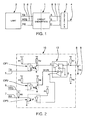
- la figure 1 est un schéma fonctionnel général montrant l'implantation du circuit d'interface selon l'invention entre un émetteur-récepteur à synchrone universel et le connecteur d'un câble de liaison;
- la figure 2 est un schéma électrique montrant un circuit d'interface connu conçu pour fonctionner en liaison série RS485;
- la figure 3 est un chronogramme illustrant le fonctionnement du circuit d'interface connu de la figure 2, en mode réception dans la partie gauche de la figure et en mode émission dans la partie droite de la figure;
- la figure 4 est un schéma électrique montrant le circuit d'interface selon l'invention, conçu pour fonctionner aussi bien en liaison série RS485 qu'en liaison série RS232;
- les figures 5 et 6 sont des chronogrammes semblables à celui de la figure 3, illustrant le fonctionnement du circuit d'interface de la figure 4 respectivement en liaison série RS485 et en liaison série RS232.
- Figure 1 is a general block diagram showing the layout of the interface circuit according to the invention between a universal synchronous transceiver and the connector of a connecting cable;
- Figure 2 is an electrical diagram showing a known interface circuit designed to operate in RS485 serial link;
- FIG. 3 is a timing diagram illustrating the operation of the interface circuit known in FIG. 2, in reception mode in the left part of the figure and in transmission mode in the right part of the figure;
- FIG. 4 is an electrical diagram showing the interface circuit according to the invention, designed to operate as well in RS485 serial link as in RS232 serial link;
- Figures 5 and 6 are timing diagrams similar to that of Figure 3, illustrating the operation of the interface circuit of Figure 4 respectively in RS485 serial link and RS232 serial link.
Dans la figure 1, le numéro de référence 1 désigne le circuit d'interface
selon l'invention, qui est intercalé entre l'émetteur-récepteur asynchrone
universel (UART) 2 d'un système hôte (non montré), par exemple un
ordinateur, et le connecteur 3 d'un câble multiconducteur 4. Le circuit
d'interface 1 est relié à l'émetteur-récepteur 2 par des conducteurs 5, 6 et
7 qui véhiculent respectivement le signal TX (données en émission en
provenance de l'émetteur-récepteur 2), le signal RTS (signal de
commande en provenance de l'émetteur-récepteur 2) et le signal RX
(données en réception vers l'émetteur-récepteur). D'autre part, le circuit
d'interface 1 est raccordé au connecteur 3 par deux conducteurs 8 et 9
pour une liaison série RS485 et, en plus des conducteurs 8 et 9, par un
troisième conducteur 11 pour une liaison série RS232. Dans le cas d'une
liaison série RS485, aussi bien les données émises en direction du câble
4 que les données reçues en provenance du câble 4 sont acheminées par
les deux conducteurs 8 et 9 sur la forme de signaux différentiels. Dans le
cas d'une liaison RS232, les données émises envoyées au câble 4 sont
acheminées par le conducteur 9, tandis que les données reçues à travers
le câble 4 sont acheminées par le conducteur 11 et, en émission comme
en réception, le potentiel présent sur le conducteur 8 est pris comme
potentiel de référence.In figure 1, the
Dans la figure 1, la ligne verticale en pointillés symbolise une isolation galvanique qui est obtenue, comme on le verra plus loin, par des coupleurs opto-électroniques. In Figure 1, the vertical dotted line symbolizes isolation galvanic which is obtained, as we will see later, by opto-electronic couplers.
La figure 2 montre un circuit d'interface connu 10, qui est conçu pour
une liaison série RS485 et qui peut être intercalé entre un émetteur-récepteur
asynchrone universel et un connecteur d'une façon semblable à
celle représentée dans la figure 1, à l'exception du conducteur 11, qui
dans ce cas, n'existe pas. Le circuit d'interface 10 comprend
essentiellement, comme composant principal, un circuit convertisseur 12
apte à convertir des signaux logiques en signaux différentiels
conformément à la norme EIA485 (RS485). Le circuit convertisseur 12
comporte une entrée de données D, une entrée de commande DE\RE une
sortie de données R, une première entrée/sortie A et une seconde
entrée/sortie B.Figure 2 shows a
L'entrée de données D est raccordée, par l'intermédiaire d'un premier
coupleur opto-électronique OP1, à la ligne 5 acheminant les données TX
émises par l'émetteur-récepteur 2. L'entrée de commande DE\RE est
raccordée, par l'intermédiaire d'un second coupleur opto-électronique
OP2, à la ligne 6 acheminant les signaux de commande RTS émis par
l'émetteur-récepteur 2. La sortie de données R est raccordée, par
l'intermédiaire d'un troisième coupleur opto-électronique OP3, à la ligne
7 acheminant à l'émetteur-récepteur 2 les données RX reçues à travers le
câble 4. L'entrée/sortie A est raccordée par le conducteur 8 à une
première broche du connecteur 3, tandis que l'autre entrée/sortie B est
raccordée par le conducteur 8 à une seconde broche du connecteur 3.Data input D is connected, via a first
opto-electronic coupler OP1, on
Dans la figure 2, les résistances R1 à R8 sont des résistances de polarisation. Les résistances R1, R3 et R5 sont connectées à une première source de tension continue Vcc1, tandis que les résistances R2, R4, R6 et R7 sont connectées à une seconde source de tension continue Vcc, et la résistance R8 à la masse. In FIG. 2, the resistors R 1 to R 8 are polarization resistors. Resistors R 1 , R 3 and R 5 are connected to a first DC voltage source Vcc1, while resistors R 2 , R 4 , R 6 and R 7 are connected to a second DC voltage source Vcc, and the resistance R 8 to ground.
Le circuit convertisseur 12 est un circuit standard sur le marché de
l'électronique, par exemple un circuit du type 75176 fabriqué notamment
par la société TEXAS INSTRUMENTS. Un tel circuit fonctionne
conformément aux tables de vérité suivantes :
L = niveau bas X = L ou H
? = indéterminé
L = low level X = L or H
? = unknown
D'après ces tables de vérité, lorsque le signal de commande présent sur
l'entrée de commande DE\RE est au niveau logique "1" ou "haut" (H),
l'entrée de données D est validée et la sortie de données R est invalidée,
c'est-à-dire qu'elle est en haute impédance. Dans ces conditions, le signal
logique présent sur l'entrée D est transmis vers le bus de données 8,9
sous la forme d'un signal différentiel, la sortie A (conducteur 8 du bus)
étant à tout instant dans le même état haut (H) ou bas (L) que l'entrée D,
et la sortie B (conducteur 9 du bus) étant dans un état bas (L) ou haut (H)
complémentaire de celui de l'entrée D.According to these truth tables, when the control signal present on
the command input DE \ RE is at logic level "1" or "high" (H),
the data input D is validated and the data output R is disabled,
that is to say, it is at high impedance. Under these conditions, the signal
logic present on input D is transmitted to the data bus 8.9
in the form of a differential signal, output A (
Inversement, lorsque le signal de commande présent sur l'entrée de
commande DE\RE est au niveau logique "0" ou "bas" (L), la sortie de
données R est validée et l'entrée D est invalidée, les bornes A et B qui
servent alors d'entrée étant en haute impédance. Dans ces conditions, un
signal différentiel arrivant aux entrées A et B en provenance du bus de
données 8,9 est transmis à la sortie R sous la forme d'un signal logique
qui est à l'état haut (H) quand l'entrée différentielle VAB est supérieure ou
égale à une valeur de seuil positive, par exemple +0,2V, et qui est à l'état
bas (L) quand l'entrée différentielle VAB est inférieure ou égale à une
valeur de seuil négative, par exemple -0,2V.Conversely, when the control signal present on the control input DE \ RE is at logic level "0" or "low" (L), the data output R is validated and the input D is invalidated, the terminals A and B which then serve as input being at high impedance. Under these conditions, a differential signal arriving at the inputs A and B coming from the
Le circuit d'interface 10 de la figure 2 fonctionne alors de la manière
illustrée par le chronogramme de la figure 3. Les signaux illustrés dans
ce chronogramme sont désignés par les mêmes symboles de référence
que ceux des points où ils apparaissent dans le circuit d'interface 10 de la
figure 2, et ils sont représentés en prenant la masse comme référence de
potentiel (0V), comme cela est indiqué pour le signal RTS dans la figure
3. The
Lorsque le signal de commande RTS provenant de l'émetteur-récepteur 2
de la figure 1 est au niveau logique "0", le système est en réception (voir
la partie gauche du chronogramme de la figure 3). C'est-à-dire que le
signal différentiel arrivant par le bus de données 8, 9 à la paire d'entrées
A et B est transmis sous la forme du signal logique RX à l'émetteur-récepteur
2. Inversement, lorsque le signal de commande RTS est au
niveau logique "1", le système est en émission (voir la partie droite du
chronogramme de la figure 3). C'est-à-dire que le signal logique TX émis
par l'émetteur-récepteur est transmis sous la forme d'un signal
différentiel aux sorties A et B et, de là, au bus de données 8,9.When the RTS control signal from
La figure 4 montre le circuit d'interface 1 selon l'invention. Dans la
figure 4, les éléments qui sont identiques ou qui jouent le même rôle que
ceux du circuit d'interface 10 de la figure 2 sont désignés par les mêmes
numéros de référence et ne seront pas décrits à nouveau en détail. Le
circuit d'interface 1 de la figure 4 diffère du circuit d'interface 10 de la
figure 2 en ce qu'il comporte deux résistances supplémentaires R9 et R10.
La résistance R9 relie à la source de tension continue Vcc l'une des
électrodes (la cathode) de l'émetteur de lumière EL (par exemple une
diode émettrice) du troisième coupleur opto-électronique OP3, qui est
raccordée à la sortie R du convertisseur 12. L'une des extrémités de la
résistance R10 est connectée à l'autre électrode de la diode émettrice de
lumière EL du coupleur opto-électronique OP3, qui est raccordée à la
source de tension continue Vcc par la résistance R6. L'autre extrémité de
la résistance R10 peut être raccordée par le conducteur 11 à l'une des
broches du connecteur 3 (figure 1). De préférence, une diode de
protection Dl est montée tête-bêche aux bornes de la diode émettrice de
lumière EL du coupleur opto-électronique OP3. Figure 4 shows the
A titre d'exemple, pour une vitesse de transmission de 9600 Bauds, les
composants du circuit d'interface 1 de la figure 4 peuvent avoir les
valeurs suivantes :
Pour un fonctionnement en liaison série RS485, seules les entrées/sorties
A et B du circuit convertisseur 12 du circuit d'interface 1 de la figure 4
sont raccordées respectivement par les conducteurs 8 et 9 au connecteur
3 du câble 4 et l'extrémité C de la résistance R10 n'est pas raccordée au
connecteur. Dans ce cas, le circuit d'interface 1 de la figure 4 fonctionne
exactement de la même manière que le circuit d'interface connu 10 de la
figure 2, comme cela est illustré par le chronogramme de la figure 5 qui
est identique au chronogramme de la figure 3. En conséquence, le
fonctionnement du circuit d'interface 1 en liaison série RS485 ne sera
pas décrit à nouveau, étant donné qu'il suffit de se référer à la
description faite plus haut à propos des figures 2 et 3. For RS485 serial link operation, only the inputs / outputs
A and B of the
Pour un fonctionnement en liaison série RS232, non seulement les deux
entrées/sorties A et B du circuit convertisseur 12 du circuit d'interface 1
sont raccordées par les conducteurs 8 et 9 à deux des broches du
connecteur 3, mais également l'extrémité C de la résistance R10 est
raccordée par le conducteur 11 à une troisième broche du connecteur 3.
Par exemple, si le connecteur 3 est un connecteur standardisé du type
DB25, les conducteurs 8,9 et 11 sont raccordés respectivement à la
broche n°7, à la broche n°2 et à la broche n°3 de ce connecteur. Les
numéros de broche sus-indiqués correspondent aux numéros réels des
broches du connecteur. Si le connecteur 3 un connecteur standardisé du
type DB9, les conducteurs 8, 9 et 11 seront raccordés respectivement à la
broche n°5, à la broche n°3 et à la broche n°2 dudit connecteur.For RS232 serial link operation, not only the two inputs / outputs A and B of the
La figure 6 est un chronogramme illustrant le fonctionnement du circuit
d'interface 1 de la figure 4 pour une liaison série RS232. Dans la figure
6, les signaux RTS, DE\RE, TX, D, R et RX sont représentés en prenant
la masse comme référence de potentiel (0V), tandis que les signaux B et
C qui apparaissent respectivement en B et C dans le circuit d'interface 1
de la figure 4, sont référencés par rapport à la broche du connecteur 3 qui
est raccordée au conducteur 8 (entrée/sortie A du circuit convertisseur
12).Figure 6 is a timing diagram illustrating the operation of the
Comme précédemment, lorsque le signal de commande RTS émis par
l'émetteur-récepteur 2 est actif (niveau logique "1"), l'émission est
validée et la réception invalidée. Inversement, lorsque le signal RTS est
inactif (niveau logique "0"), l'émission est invalidée et la réception
validée.As before, when the RTS control signal emitted by
L'émission en RS232 (voir la partie droite du chronogramme de la figure
6) s'effectue sur la sortie B du circuit convertisseur 12 qui est référencée
par rapport à l'entrée/sortie A. Plus précisément, lorsque le signal TX
émis par l'émetteur-récepteur 2 est actif (masse ou 0V), le signal B sera
actif (tension positive en émission RS232) tandis que, lorsque le signal
TX est inactif (Vcc), le signal B sera inactif (tension négative en
émission RS232), comme montré dans la partie droite du chronogramme
de la figure 6.The transmission in RS232 (see the right part of the timing diagram in the figure
6) takes place on the output B of the
La réception en RS232 (voir la partie gauche du chronogramme de la
figure 6) s'effectue sur le conducteur 11 (signal C), tout en étant
référencée par rapport à la broche du connecteur 3 qui est raccordée au
conducteur 8 (entrée/sortie A). Plus précisément, lorsque le signal C
arrivant sur le conducteur 11 a un niveau passif ou inactif (tension
négative en réception RS232), il bloquera le coupleur opto-électronique
OP3, de sorte que le signal RX prend un niveau logique "1".
Inversement, lorsque le signal C a un niveau actif (tension positive en
réception RS232), il fera conduire le coupleur opto-électronique OP3, de
sorte que le signal RX prend un niveau logique "0" comme montré dans
la partie gauche du chronogramme de la figure 6.Reception in RS232 (see the left part of the timing diagram of the
Figure 6) is carried out on the conductor 11 (signal C), while being
referenced with respect to the
Ainsi, d'après ce qui précède, on voit que le circuit d'interface 1 selon
l'invention, obtenu en ajoutant simplement deux résistances (R9 et R10)
au circuit d'interface connu 10 de la figure 2, peut être utilisé pour
émettre et recevoir des données conformément au standard RS485 ou
conformément au standard RS232 simplement en changeant le câblage
du connecteur 3. En pratique, il suffit de prévoir un premier câble 4 muni
d'un connecteur 3 dont deux des broches sont raccordées respectivement
aux conducteurs 8 et 9 pour une transmission selon le standard RS485, et
un second câble 4 muni d'un connecteur 3 dont trois des broches sont
raccordées respectivement aux conducteurs 8, 9 et 11 pour une
transmission selon le standard RS232. Ainsi, le circuit d'interface selon
l'invention pourra être raccordé à des machines ou appareils prévus pour
communiquer selon le standard RS485 en utilisant le premier câble, ou à
des machines ou appareils prévus pour communiquer selon le standard
RS232 en utilisant le second câble. Ceci représente un grand avantage
dans la mesure où il n'est plus nécessaire de changer une carte dans le
système hôte, dans lequel est incorporé le circuit d'interface selon
l'invention, pour que ce système hôte puisse communiquer avec des
machines ou appareils externes ou éloignés selon le standard RS485 ou
le standard RS232.Thus, from the above, we see that the
Il va de soi que le mode de réalisation qui a été décrit ci-dessus, a été
donné à titre de d'exemple purement indicatif et nullement limitatif et
que diverses modifications peuvent être apportées par l'homme de l'art
sans pour autant sortir du cadre de l'invention. C'est ainsi notamment que
les valeurs des tensions continues, les valeurs ohmiques des résistances
R1 à R10, les composants électroniques OP1, OP2, OP3, D1 et le circuit
convertisseur 12 peuvent être différents de ceux qui ont été indiqués plus
haut, ces valeurs et composants pouvant dépendre de divers paramètres,
en particulier de la vitesse désirée de transmission des données, la
longueur maximale du câble 4 à utiliser, etc...It goes without saying that the embodiment which has been described above has been
given by way of example purely indicative and in no way limitative and
that various modifications can be made by those skilled in the art
without departing from the scope of the invention. This is how in particular
the values of the DC voltages, the ohmic values of the resistances
R1 to R10, the electronic components OP1, OP2, OP3, D1 and the
Claims (2)
Applications Claiming Priority (2)
| Application Number | Priority Date | Filing Date | Title |
|---|---|---|---|
| FR9806878A FR2779250B1 (en) | 1998-06-02 | 1998-06-02 | BISTANDARD INTERFACE CIRCUIT FOR SERIAL LINK |
| FR9806878 | 1998-06-02 |
Publications (2)
| Publication Number | Publication Date |
|---|---|
| EP0962869A1 true EP0962869A1 (en) | 1999-12-08 |
| EP0962869B1 EP0962869B1 (en) | 2004-03-10 |
Family
ID=9526917
Family Applications (1)
| Application Number | Title | Priority Date | Filing Date |
|---|---|---|---|
| EP19990401203 Expired - Lifetime EP0962869B1 (en) | 1998-06-02 | 1999-05-19 | Dual-standard interface circuit for serial link |
Country Status (3)
| Country | Link |
|---|---|
| EP (1) | EP0962869B1 (en) |
| DE (1) | DE69915410T2 (en) |
| FR (1) | FR2779250B1 (en) |
Cited By (10)
| Publication number | Priority date | Publication date | Assignee | Title |
|---|---|---|---|---|
| EP1199857A2 (en) * | 2000-09-21 | 2002-04-24 | Infineon Technologies AG | Tristate driver |
| CN101895289A (en) * | 2010-07-05 | 2010-11-24 | 艾默生网络能源有限公司 | Signal interface circuit |
| CN103227636A (en) * | 2013-03-27 | 2013-07-31 | 武汉新慧电气科技有限公司 | High-isolation direct splicing half-duplex communication interface module for interconnection of multiple controllers |
| CN103633985A (en) * | 2013-12-11 | 2014-03-12 | 济南诺辉节能技术开发有限公司 | RS485 communication circuit |
| CN103701452A (en) * | 2012-09-27 | 2014-04-02 | 深圳市朗驰欣创科技有限公司 | Multifunctional communication interface signal converter |
| CN105159194A (en) * | 2015-08-25 | 2015-12-16 | 天津市英贝特航天科技有限公司 | Switching circuit and switching method for switching data receiving/sending operation of RS-485 serial port |
| CN111630780A (en) * | 2018-10-26 | 2020-09-04 | 深圳配天智能技术研究院有限公司 | Conversion circuit, adapter plate and control system |
| CN114925006A (en) * | 2022-05-06 | 2022-08-19 | 青岛艾诺智能仪器有限公司 | Semi-passive RS 232-to-RS 232 communication method |
| WO2023087986A1 (en) * | 2021-11-22 | 2023-05-25 | 江苏科技大学 | Shared-485 circuit and control method |
| CN116340238A (en) * | 2023-03-28 | 2023-06-27 | 怀化建南机器厂有限公司 | Interface circuit of MCU serial port and RS485 converter |
Families Citing this family (1)
| Publication number | Priority date | Publication date | Assignee | Title |
|---|---|---|---|---|
| CN102915291B (en) * | 2012-09-29 | 2016-03-30 | 无锡华润矽科微电子有限公司 | A kind of RS485 interface circuit with automatic reverse function |
Citations (2)
| Publication number | Priority date | Publication date | Assignee | Title |
|---|---|---|---|---|
| DE4113920A1 (en) * | 1991-04-29 | 1992-11-05 | Ulrich Karstein Datentechnik | Data exchange set=up between personal computer and programmable memory - uses multipole connectors with interface circuitry and control circuits for serial transmissions |
| DE4133636A1 (en) * | 1991-10-11 | 1993-04-15 | Lawrenz Wolfhard | CONTROL BLOCK |
-
1998
- 1998-06-02 FR FR9806878A patent/FR2779250B1/en not_active Expired - Fee Related
-
1999
- 1999-05-19 EP EP19990401203 patent/EP0962869B1/en not_active Expired - Lifetime
- 1999-05-19 DE DE69915410T patent/DE69915410T2/en not_active Expired - Lifetime
Patent Citations (2)
| Publication number | Priority date | Publication date | Assignee | Title |
|---|---|---|---|---|
| DE4113920A1 (en) * | 1991-04-29 | 1992-11-05 | Ulrich Karstein Datentechnik | Data exchange set=up between personal computer and programmable memory - uses multipole connectors with interface circuitry and control circuits for serial transmissions |
| DE4133636A1 (en) * | 1991-10-11 | 1993-04-15 | Lawrenz Wolfhard | CONTROL BLOCK |
Non-Patent Citations (2)
| Title |
|---|
| BARREAU A.: "Versatile optoelectronic logic circuit elements", ELECTRONIC ENGINEERING., vol. 58, no. 712, April 1986 (1986-04-01), LONDON GB, pages 39 - 46, XP002097127 * |
| HANS SORENSEN: "Opto-isolator developments are making your design chores simpler.", EDN ELECTRICAL DESIGN NEWS., vol. 18, no. 24, 20 December 1973 (1973-12-20), NEWTON, MASSACHUSETTS US, pages 36 - 44, XP002097128 * |
Cited By (13)
| Publication number | Priority date | Publication date | Assignee | Title |
|---|---|---|---|---|
| EP1199857A2 (en) * | 2000-09-21 | 2002-04-24 | Infineon Technologies AG | Tristate driver |
| EP1199857A3 (en) * | 2000-09-21 | 2006-06-21 | Infineon Technologies AG | Tristate driver |
| CN101895289A (en) * | 2010-07-05 | 2010-11-24 | 艾默生网络能源有限公司 | Signal interface circuit |
| CN103701452A (en) * | 2012-09-27 | 2014-04-02 | 深圳市朗驰欣创科技有限公司 | Multifunctional communication interface signal converter |
| CN103227636A (en) * | 2013-03-27 | 2013-07-31 | 武汉新慧电气科技有限公司 | High-isolation direct splicing half-duplex communication interface module for interconnection of multiple controllers |
| CN103633985A (en) * | 2013-12-11 | 2014-03-12 | 济南诺辉节能技术开发有限公司 | RS485 communication circuit |
| CN105159194A (en) * | 2015-08-25 | 2015-12-16 | 天津市英贝特航天科技有限公司 | Switching circuit and switching method for switching data receiving/sending operation of RS-485 serial port |
| CN111630780A (en) * | 2018-10-26 | 2020-09-04 | 深圳配天智能技术研究院有限公司 | Conversion circuit, adapter plate and control system |
| WO2023087986A1 (en) * | 2021-11-22 | 2023-05-25 | 江苏科技大学 | Shared-485 circuit and control method |
| CN114925006A (en) * | 2022-05-06 | 2022-08-19 | 青岛艾诺智能仪器有限公司 | Semi-passive RS 232-to-RS 232 communication method |
| CN114925006B (en) * | 2022-05-06 | 2024-03-05 | 青岛艾诺仪器有限公司 | Semi-passive RS 232-to-RS 232 communication method |
| CN116340238A (en) * | 2023-03-28 | 2023-06-27 | 怀化建南机器厂有限公司 | Interface circuit of MCU serial port and RS485 converter |
| CN116340238B (en) * | 2023-03-28 | 2024-01-30 | 怀化建南机器厂有限公司 | Interface circuit of MCU serial port and RS485 converter |
Also Published As
| Publication number | Publication date |
|---|---|
| FR2779250A1 (en) | 1999-12-03 |
| DE69915410T2 (en) | 2005-02-17 |
| EP0962869B1 (en) | 2004-03-10 |
| FR2779250B1 (en) | 2001-09-07 |
| DE69915410D1 (en) | 2004-04-15 |
Similar Documents
| Publication | Publication Date | Title |
|---|---|---|
| EP0962869B1 (en) | Dual-standard interface circuit for serial link | |
| JP5223183B2 (en) | Opto-electric composite wiring component and electronic device using the same | |
| US9225423B1 (en) | Optical engines and optical cable assemblies capable of low-speed and high-speed optical communication | |
| CA2620025A1 (en) | Optical communication bus network for avionic equipment | |
| WO2017005361A1 (en) | Transmitter-receiver device connectable to a communications network by a can-type or flexray-type bus | |
| CA2763011C (en) | Wireless two-way transmission of serial data signals between an electronic device and a power meter | |
| EP1668804A1 (en) | Single-channel communication device for optical fibre | |
| EP0246132A1 (en) | Bidirectional interface circuit presenting a unipolar and a bipolar acces for logical signals | |
| EP0735706B1 (en) | Interface device | |
| EP3248305B1 (en) | Ethernet switch for fiberoptic network | |
| US20160080843A1 (en) | Optical engines and optical cable assemblies having electrical signal conditioning | |
| EP0002971A1 (en) | Coupling device for an optical transmission line and transmission system comprising such device | |
| US7317934B2 (en) | Configurable communications modules and methods of making the same | |
| EP0128800B1 (en) | Optical quadripole and multipole comprised of such a quadripole | |
| EP2658151A1 (en) | Communication device to connect a user facility to an optical fiber | |
| FR2776443A1 (en) | Electrical isolation circuit between a bi-directional universal serial bus and a peripheral circuit | |
| EP1100231B1 (en) | Device and connection box for a local network | |
| EP1059706B1 (en) | Device for the connection of electronic units or modules | |
| EP0388846A1 (en) | Laser feeding and controlling apparatus for an optical fibre link between a subscriber and a telecommunication exchange | |
| US20050152704A1 (en) | Implementation of gradual impedance gradient transmission line for optimized matching in fiber optic transmitter laser drivers | |
| EP1309088A1 (en) | Switching device equipped with polarity inversion means | |
| WO2013164533A1 (en) | Electronic control unit having a configurable line termination | |
| FR2585510A1 (en) | Device for coupling several electric signal-input paths to the same electric output path with insulation of the earths | |
| FR2942063A3 (en) | Device for ensuring connection and dialogue between e.g. personal digital assistant and electronic energy meter, has wired connection for realizing direction connection between computer and energy meter and with electronic interface | |
| FR2524230A1 (en) | Information transmission system for optical fibre link - uses generator to modulate information signal with service signals, and low pass filter to maintain constant output of laser diode |
Legal Events
| Date | Code | Title | Description |
|---|---|---|---|
| PUAI | Public reference made under article 153(3) epc to a published international application that has entered the european phase |
Free format text: ORIGINAL CODE: 0009012 |
|
| AK | Designated contracting states |
Kind code of ref document: A1 Designated state(s): CH DE ES FR IT LI |
|
| AX | Request for extension of the european patent |
Free format text: AL;LT;LV;MK;RO;SI |
|
| 17P | Request for examination filed |
Effective date: 20000519 |
|
| AKX | Designation fees paid |
Free format text: CH DE ES FR IT LI |
|
| GRAP | Despatch of communication of intention to grant a patent |
Free format text: ORIGINAL CODE: EPIDOSNIGR1 |
|
| GRAS | Grant fee paid |
Free format text: ORIGINAL CODE: EPIDOSNIGR3 |
|
| GRAA | (expected) grant |
Free format text: ORIGINAL CODE: 0009210 |
|
| AK | Designated contracting states |
Kind code of ref document: B1 Designated state(s): CH DE ES FR IT LI |
|
| PG25 | Lapsed in a contracting state [announced via postgrant information from national office to epo] |
Ref country code: IT Free format text: LAPSE BECAUSE OF FAILURE TO SUBMIT A TRANSLATION OF THE DESCRIPTION OR TO PAY THE FEE WITHIN THE PRESCRIBED TIME-LIMIT;WARNING: LAPSES OF ITALIAN PATENTS WITH EFFECTIVE DATE BEFORE 2007 MAY HAVE OCCURRED AT ANY TIME BEFORE 2007. THE CORRECT EFFECTIVE DATE MAY BE DIFFERENT FROM THE ONE RECORDED. Effective date: 20040310 |
|
| REG | Reference to a national code |
Ref country code: CH Ref legal event code: EP |
|
| REF | Corresponds to: |
Ref document number: 69915410 Country of ref document: DE Date of ref document: 20040415 Kind code of ref document: P |
|
| PG25 | Lapsed in a contracting state [announced via postgrant information from national office to epo] |
Ref country code: LI Free format text: LAPSE BECAUSE OF NON-PAYMENT OF DUE FEES Effective date: 20040531 Ref country code: CH Free format text: LAPSE BECAUSE OF NON-PAYMENT OF DUE FEES Effective date: 20040531 |
|
| PG25 | Lapsed in a contracting state [announced via postgrant information from national office to epo] |
Ref country code: ES Free format text: LAPSE BECAUSE OF FAILURE TO SUBMIT A TRANSLATION OF THE DESCRIPTION OR TO PAY THE FEE WITHIN THE PRESCRIBED TIME-LIMIT Effective date: 20040621 |
|
| PLBE | No opposition filed within time limit |
Free format text: ORIGINAL CODE: 0009261 |
|
| REG | Reference to a national code |
Ref country code: CH Ref legal event code: PL |
|
| STAA | Information on the status of an ep patent application or granted ep patent |
Free format text: STATUS: NO OPPOSITION FILED WITHIN TIME LIMIT |
|
| 26N | No opposition filed |
Effective date: 20041213 |
|
| REG | Reference to a national code |
Ref country code: FR Ref legal event code: PLFP Year of fee payment: 18 |
|
| PGFP | Annual fee paid to national office [announced via postgrant information from national office to epo] |
Ref country code: FR Payment date: 20160520 Year of fee payment: 18 |
|
| REG | Reference to a national code |
Ref country code: FR Ref legal event code: ST Effective date: 20180131 |
|
| PG25 | Lapsed in a contracting state [announced via postgrant information from national office to epo] |
Ref country code: FR Free format text: LAPSE BECAUSE OF NON-PAYMENT OF DUE FEES Effective date: 20170531 |
|
| PGFP | Annual fee paid to national office [announced via postgrant information from national office to epo] |
Ref country code: DE Payment date: 20180522 Year of fee payment: 20 |
|
| REG | Reference to a national code |
Ref country code: DE Ref legal event code: R071 Ref document number: 69915410 Country of ref document: DE |