EP0962320B1 - Ink-Jet head, ink-jet head substrate, and a method for making the head - Google Patents
Ink-Jet head, ink-jet head substrate, and a method for making the head Download PDFInfo
- Publication number
- EP0962320B1 EP0962320B1 EP99110640A EP99110640A EP0962320B1 EP 0962320 B1 EP0962320 B1 EP 0962320B1 EP 99110640 A EP99110640 A EP 99110640A EP 99110640 A EP99110640 A EP 99110640A EP 0962320 B1 EP0962320 B1 EP 0962320B1
- Authority
- EP
- European Patent Office
- Prior art keywords
- ink
- substrate
- jet head
- layer
- liquid channel
- Prior art date
- Legal status (The legal status is an assumption and is not a legal conclusion. Google has not performed a legal analysis and makes no representation as to the accuracy of the status listed.)
- Expired - Lifetime
Links
- 239000000758 substrate Substances 0.000 title claims description 105
- 238000000034 method Methods 0.000 title claims description 41
- 239000010410 layer Substances 0.000 claims description 102
- 229920002614 Polyether block amide Polymers 0.000 claims description 88
- 229920005989 resin Polymers 0.000 claims description 36
- 239000011347 resin Substances 0.000 claims description 36
- 239000007788 liquid Substances 0.000 claims description 35
- 239000011241 protective layer Substances 0.000 claims description 35
- 230000008569 process Effects 0.000 claims description 27
- 238000007599 discharging Methods 0.000 claims description 15
- 239000013557 residual solvent Substances 0.000 claims description 14
- 239000003822 epoxy resin Substances 0.000 claims description 12
- 229920000647 polyepoxide Polymers 0.000 claims description 12
- 238000004380 ashing Methods 0.000 claims description 8
- QVGXLLKOCUKJST-UHFFFAOYSA-N atomic oxygen Chemical compound [O] QVGXLLKOCUKJST-UHFFFAOYSA-N 0.000 claims description 8
- 239000001301 oxygen Substances 0.000 claims description 8
- 229910052760 oxygen Inorganic materials 0.000 claims description 8
- 239000002904 solvent Substances 0.000 claims description 7
- 238000000465 moulding Methods 0.000 claims description 5
- 238000010538 cationic polymerization reaction Methods 0.000 claims description 4
- 230000000694 effects Effects 0.000 claims description 4
- 229920002492 poly(sulfone) Polymers 0.000 claims description 4
- 239000004721 Polyphenylene oxide Substances 0.000 claims description 3
- 238000000059 patterning Methods 0.000 claims description 3
- 229920000570 polyether Polymers 0.000 claims description 3
- 230000001681 protective effect Effects 0.000 claims description 3
- 229920001169 thermoplastic Polymers 0.000 claims description 3
- 239000004416 thermosoftening plastic Substances 0.000 claims description 3
- 239000004695 Polyether sulfone Substances 0.000 claims description 2
- 229920006393 polyether sulfone Polymers 0.000 claims description 2
- 238000003466 welding Methods 0.000 claims description 2
- 150000001875 compounds Chemical class 0.000 claims 2
- 238000001291 vacuum drying Methods 0.000 claims 1
- 239000000976 ink Substances 0.000 description 78
- 229910052716 thallium Inorganic materials 0.000 description 18
- BKVIYDNLLOSFOA-UHFFFAOYSA-N thallium Chemical compound [Tl] BKVIYDNLLOSFOA-UHFFFAOYSA-N 0.000 description 18
- 238000012360 testing method Methods 0.000 description 17
- VYPSYNLAJGMNEJ-UHFFFAOYSA-N Silicium dioxide Chemical compound O=[Si]=O VYPSYNLAJGMNEJ-UHFFFAOYSA-N 0.000 description 15
- 229910052814 silicon oxide Inorganic materials 0.000 description 15
- 238000002474 experimental method Methods 0.000 description 14
- 229920001721 polyimide Polymers 0.000 description 12
- 229910052782 aluminium Inorganic materials 0.000 description 10
- XAGFODPZIPBFFR-UHFFFAOYSA-N aluminium Chemical compound [Al] XAGFODPZIPBFFR-UHFFFAOYSA-N 0.000 description 10
- 239000000243 solution Substances 0.000 description 10
- 229920002120 photoresistant polymer Polymers 0.000 description 9
- XSQUKJJJFZCRTK-UHFFFAOYSA-N Urea Chemical compound NC(N)=O XSQUKJJJFZCRTK-UHFFFAOYSA-N 0.000 description 8
- 239000004202 carbamide Substances 0.000 description 8
- 239000002798 polar solvent Substances 0.000 description 8
- 239000004642 Polyimide Substances 0.000 description 7
- XUIMIQQOPSSXEZ-UHFFFAOYSA-N Silicon Chemical compound [Si] XUIMIQQOPSSXEZ-UHFFFAOYSA-N 0.000 description 7
- 230000007797 corrosion Effects 0.000 description 7
- 238000005260 corrosion Methods 0.000 description 7
- 239000000463 material Substances 0.000 description 7
- 238000000926 separation method Methods 0.000 description 7
- 239000010703 silicon Substances 0.000 description 7
- 229910052710 silicon Inorganic materials 0.000 description 7
- LYCAIKOWRPUZTN-UHFFFAOYSA-N Ethylene glycol Chemical compound OCCO LYCAIKOWRPUZTN-UHFFFAOYSA-N 0.000 description 6
- 230000008859 change Effects 0.000 description 6
- 239000011521 glass Substances 0.000 description 6
- 238000004321 preservation Methods 0.000 description 6
- ZNQVEEAIQZEUHB-UHFFFAOYSA-N 2-ethoxyethanol Chemical compound CCOCCO ZNQVEEAIQZEUHB-UHFFFAOYSA-N 0.000 description 5
- 239000007787 solid Substances 0.000 description 5
- 238000004544 sputter deposition Methods 0.000 description 5
- 239000002344 surface layer Substances 0.000 description 5
- 230000009477 glass transition Effects 0.000 description 4
- 239000009719 polyimide resin Substances 0.000 description 4
- 230000004044 response Effects 0.000 description 4
- 238000004528 spin coating Methods 0.000 description 4
- XLYOFNOQVPJJNP-UHFFFAOYSA-N water Substances O XLYOFNOQVPJJNP-UHFFFAOYSA-N 0.000 description 4
- 229910003862 HfB2 Inorganic materials 0.000 description 3
- SECXISVLQFMRJM-UHFFFAOYSA-N N-Methylpyrrolidone Chemical compound CN1CCCC1=O SECXISVLQFMRJM-UHFFFAOYSA-N 0.000 description 3
- 230000015572 biosynthetic process Effects 0.000 description 3
- 238000004090 dissolution Methods 0.000 description 3
- 238000001035 drying Methods 0.000 description 3
- 238000005530 etching Methods 0.000 description 3
- 238000010438 heat treatment Methods 0.000 description 3
- 239000000203 mixture Substances 0.000 description 3
- 239000012044 organic layer Substances 0.000 description 3
- 230000003647 oxidation Effects 0.000 description 3
- 238000007254 oxidation reaction Methods 0.000 description 3
- 238000007639 printing Methods 0.000 description 3
- NQBXSWAWVZHKBZ-UHFFFAOYSA-N 2-butoxyethyl acetate Chemical compound CCCCOCCOC(C)=O NQBXSWAWVZHKBZ-UHFFFAOYSA-N 0.000 description 2
- RYGMFSIKBFXOCR-UHFFFAOYSA-N Copper Chemical compound [Cu] RYGMFSIKBFXOCR-UHFFFAOYSA-N 0.000 description 2
- KRHYYFGTRYWZRS-UHFFFAOYSA-N Fluorane Chemical compound F KRHYYFGTRYWZRS-UHFFFAOYSA-N 0.000 description 2
- 239000004952 Polyamide Substances 0.000 description 2
- 239000006087 Silane Coupling Agent Substances 0.000 description 2
- 239000012670 alkaline solution Substances 0.000 description 2
- JNDMLEXHDPKVFC-UHFFFAOYSA-N aluminum;oxygen(2-);yttrium(3+) Chemical compound [O-2].[O-2].[O-2].[Al+3].[Y+3] JNDMLEXHDPKVFC-UHFFFAOYSA-N 0.000 description 2
- 239000012298 atmosphere Substances 0.000 description 2
- 230000000052 comparative effect Effects 0.000 description 2
- 229910052802 copper Inorganic materials 0.000 description 2
- 239000010949 copper Substances 0.000 description 2
- 238000005336 cracking Methods 0.000 description 2
- 238000005520 cutting process Methods 0.000 description 2
- 238000000313 electron-beam-induced deposition Methods 0.000 description 2
- 238000004817 gas chromatography Methods 0.000 description 2
- 239000003906 humectant Substances 0.000 description 2
- 238000007654 immersion Methods 0.000 description 2
- 150000002500 ions Chemical class 0.000 description 2
- KFZMGEQAYNKOFK-UHFFFAOYSA-N isopropyl alcohol Natural products CC(C)O KFZMGEQAYNKOFK-UHFFFAOYSA-N 0.000 description 2
- CNQCVBJFEGMYDW-UHFFFAOYSA-N lawrencium atom Chemical compound [Lr] CNQCVBJFEGMYDW-UHFFFAOYSA-N 0.000 description 2
- 229910052751 metal Inorganic materials 0.000 description 2
- 239000002184 metal Substances 0.000 description 2
- 239000007769 metal material Substances 0.000 description 2
- 229920003986 novolac Polymers 0.000 description 2
- 229920002647 polyamide Polymers 0.000 description 2
- 239000010936 titanium Substances 0.000 description 2
- 229910019901 yttrium aluminum garnet Inorganic materials 0.000 description 2
- JYEUMXHLPRZUAT-UHFFFAOYSA-N 1,2,3-triazine Chemical compound C1=CN=NN=C1 JYEUMXHLPRZUAT-UHFFFAOYSA-N 0.000 description 1
- DDFHBQSCUXNBSA-UHFFFAOYSA-N 5-(5-carboxythiophen-2-yl)thiophene-2-carboxylic acid Chemical compound S1C(C(=O)O)=CC=C1C1=CC=C(C(O)=O)S1 DDFHBQSCUXNBSA-UHFFFAOYSA-N 0.000 description 1
- 229910000906 Bronze Inorganic materials 0.000 description 1
- 239000004593 Epoxy Substances 0.000 description 1
- NTIZESTWPVYFNL-UHFFFAOYSA-N Methyl isobutyl ketone Chemical compound CC(C)CC(C)=O NTIZESTWPVYFNL-UHFFFAOYSA-N 0.000 description 1
- UIHCLUNTQKBZGK-UHFFFAOYSA-N Methyl isobutyl ketone Natural products CCC(C)C(C)=O UIHCLUNTQKBZGK-UHFFFAOYSA-N 0.000 description 1
- CTQNGGLPUBDAKN-UHFFFAOYSA-N O-Xylene Chemical compound CC1=CC=CC=C1C CTQNGGLPUBDAKN-UHFFFAOYSA-N 0.000 description 1
- OAICVXFJPJFONN-UHFFFAOYSA-N Phosphorus Chemical compound [P] OAICVXFJPJFONN-UHFFFAOYSA-N 0.000 description 1
- RTAQQCXQSZGOHL-UHFFFAOYSA-N Titanium Chemical compound [Ti] RTAQQCXQSZGOHL-UHFFFAOYSA-N 0.000 description 1
- 238000009825 accumulation Methods 0.000 description 1
- 230000002411 adverse Effects 0.000 description 1
- 238000009835 boiling Methods 0.000 description 1
- 239000010974 bronze Substances 0.000 description 1
- 239000000919 ceramic Substances 0.000 description 1
- BGTFCAQCKWKTRL-YDEUACAXSA-N chembl1095986 Chemical compound C1[C@@H](N)[C@@H](O)[C@H](C)O[C@H]1O[C@@H]([C@H]1C(N[C@H](C2=CC(O)=CC(O[C@@H]3[C@H]([C@@H](O)[C@H](O)[C@@H](CO)O3)O)=C2C=2C(O)=CC=C(C=2)[C@@H](NC(=O)[C@@H]2NC(=O)[C@@H]3C=4C=C(C(=C(O)C=4)C)OC=4C(O)=CC=C(C=4)[C@@H](N)C(=O)N[C@@H](C(=O)N3)[C@H](O)C=3C=CC(O4)=CC=3)C(=O)N1)C(O)=O)=O)C(C=C1)=CC=C1OC1=C(O[C@@H]3[C@H]([C@H](O)[C@@H](O)[C@H](CO[C@@H]5[C@H]([C@@H](O)[C@H](O)[C@@H](C)O5)O)O3)O[C@@H]3[C@H]([C@@H](O)[C@H](O)[C@@H](CO)O3)O[C@@H]3[C@H]([C@H](O)[C@@H](CO)O3)O)C4=CC2=C1 BGTFCAQCKWKTRL-YDEUACAXSA-N 0.000 description 1
- 239000011248 coating agent Substances 0.000 description 1
- 238000000576 coating method Methods 0.000 description 1
- KUNSUQLRTQLHQQ-UHFFFAOYSA-N copper tin Chemical compound [Cu].[Sn] KUNSUQLRTQLHQQ-UHFFFAOYSA-N 0.000 description 1
- 239000013078 crystal Substances 0.000 description 1
- 230000003247 decreasing effect Effects 0.000 description 1
- 230000007547 defect Effects 0.000 description 1
- 230000006866 deterioration Effects 0.000 description 1
- 230000008034 disappearance Effects 0.000 description 1
- 238000001312 dry etching Methods 0.000 description 1
- 238000005516 engineering process Methods 0.000 description 1
- 238000001704 evaporation Methods 0.000 description 1
- 230000008020 evaporation Effects 0.000 description 1
- PCHJSUWPFVWCPO-UHFFFAOYSA-N gold Chemical compound [Au] PCHJSUWPFVWCPO-UHFFFAOYSA-N 0.000 description 1
- 239000010931 gold Substances 0.000 description 1
- 229910052737 gold Inorganic materials 0.000 description 1
- LNEPOXFFQSENCJ-UHFFFAOYSA-N haloperidol Chemical compound C1CC(O)(C=2C=CC(Cl)=CC=2)CCN1CCCC(=O)C1=CC=C(F)C=C1 LNEPOXFFQSENCJ-UHFFFAOYSA-N 0.000 description 1
- 230000012447 hatching Effects 0.000 description 1
- 230000007062 hydrolysis Effects 0.000 description 1
- 238000006460 hydrolysis reaction Methods 0.000 description 1
- 238000009413 insulation Methods 0.000 description 1
- 239000012212 insulator Substances 0.000 description 1
- 125000001449 isopropyl group Chemical group [H]C([H])([H])C([H])(*)C([H])([H])[H] 0.000 description 1
- 230000007774 longterm Effects 0.000 description 1
- 238000004519 manufacturing process Methods 0.000 description 1
- 238000005259 measurement Methods 0.000 description 1
- 239000012528 membrane Substances 0.000 description 1
- 239000012046 mixed solvent Substances 0.000 description 1
- 238000012986 modification Methods 0.000 description 1
- 230000004048 modification Effects 0.000 description 1
- 230000007935 neutral effect Effects 0.000 description 1
- 239000012454 non-polar solvent Substances 0.000 description 1
- 230000003287 optical effect Effects 0.000 description 1
- 239000011368 organic material Substances 0.000 description 1
- 239000012466 permeate Substances 0.000 description 1
- 239000005011 phenolic resin Substances 0.000 description 1
- 239000000049 pigment Substances 0.000 description 1
- 238000000623 plasma-assisted chemical vapour deposition Methods 0.000 description 1
- 229920006122 polyamide resin Polymers 0.000 description 1
- 229920000642 polymer Polymers 0.000 description 1
- 239000002685 polymerization catalyst Substances 0.000 description 1
- 238000001556 precipitation Methods 0.000 description 1
- 238000003825 pressing Methods 0.000 description 1
- 238000011160 research Methods 0.000 description 1
- 229920002050 silicone resin Polymers 0.000 description 1
- 239000000126 substance Substances 0.000 description 1
- 229910052719 titanium Inorganic materials 0.000 description 1
- 239000008096 xylene Substances 0.000 description 1
Images


Classifications
-
- B—PERFORMING OPERATIONS; TRANSPORTING
- B41—PRINTING; LINING MACHINES; TYPEWRITERS; STAMPS
- B41J—TYPEWRITERS; SELECTIVE PRINTING MECHANISMS, i.e. MECHANISMS PRINTING OTHERWISE THAN FROM A FORME; CORRECTION OF TYPOGRAPHICAL ERRORS
- B41J2/00—Typewriters or selective printing mechanisms characterised by the printing or marking process for which they are designed
- B41J2/005—Typewriters or selective printing mechanisms characterised by the printing or marking process for which they are designed characterised by bringing liquid or particles selectively into contact with a printing material
- B41J2/01—Ink jet
- B41J2/135—Nozzles
- B41J2/16—Production of nozzles
- B41J2/1621—Manufacturing processes
- B41J2/164—Manufacturing processes thin film formation
- B41J2/1642—Manufacturing processes thin film formation thin film formation by CVD [chemical vapor deposition]
-
- B—PERFORMING OPERATIONS; TRANSPORTING
- B41—PRINTING; LINING MACHINES; TYPEWRITERS; STAMPS
- B41J—TYPEWRITERS; SELECTIVE PRINTING MECHANISMS, i.e. MECHANISMS PRINTING OTHERWISE THAN FROM A FORME; CORRECTION OF TYPOGRAPHICAL ERRORS
- B41J2/00—Typewriters or selective printing mechanisms characterised by the printing or marking process for which they are designed
- B41J2/005—Typewriters or selective printing mechanisms characterised by the printing or marking process for which they are designed characterised by bringing liquid or particles selectively into contact with a printing material
- B41J2/01—Ink jet
- B41J2/135—Nozzles
- B41J2/14—Structure thereof only for on-demand ink jet heads
- B41J2/14016—Structure of bubble jet print heads
- B41J2/14088—Structure of heating means
- B41J2/14112—Resistive element
- B41J2/14129—Layer structure
-
- B—PERFORMING OPERATIONS; TRANSPORTING
- B41—PRINTING; LINING MACHINES; TYPEWRITERS; STAMPS
- B41J—TYPEWRITERS; SELECTIVE PRINTING MECHANISMS, i.e. MECHANISMS PRINTING OTHERWISE THAN FROM A FORME; CORRECTION OF TYPOGRAPHICAL ERRORS
- B41J2/00—Typewriters or selective printing mechanisms characterised by the printing or marking process for which they are designed
- B41J2/005—Typewriters or selective printing mechanisms characterised by the printing or marking process for which they are designed characterised by bringing liquid or particles selectively into contact with a printing material
- B41J2/01—Ink jet
- B41J2/135—Nozzles
- B41J2/16—Production of nozzles
- B41J2/1601—Production of bubble jet print heads
-
- B—PERFORMING OPERATIONS; TRANSPORTING
- B41—PRINTING; LINING MACHINES; TYPEWRITERS; STAMPS
- B41J—TYPEWRITERS; SELECTIVE PRINTING MECHANISMS, i.e. MECHANISMS PRINTING OTHERWISE THAN FROM A FORME; CORRECTION OF TYPOGRAPHICAL ERRORS
- B41J2/00—Typewriters or selective printing mechanisms characterised by the printing or marking process for which they are designed
- B41J2/005—Typewriters or selective printing mechanisms characterised by the printing or marking process for which they are designed characterised by bringing liquid or particles selectively into contact with a printing material
- B41J2/01—Ink jet
- B41J2/135—Nozzles
- B41J2/16—Production of nozzles
- B41J2/1621—Manufacturing processes
- B41J2/1623—Manufacturing processes bonding and adhesion
-
- B—PERFORMING OPERATIONS; TRANSPORTING
- B41—PRINTING; LINING MACHINES; TYPEWRITERS; STAMPS
- B41J—TYPEWRITERS; SELECTIVE PRINTING MECHANISMS, i.e. MECHANISMS PRINTING OTHERWISE THAN FROM A FORME; CORRECTION OF TYPOGRAPHICAL ERRORS
- B41J2/00—Typewriters or selective printing mechanisms characterised by the printing or marking process for which they are designed
- B41J2/005—Typewriters or selective printing mechanisms characterised by the printing or marking process for which they are designed characterised by bringing liquid or particles selectively into contact with a printing material
- B41J2/01—Ink jet
- B41J2/135—Nozzles
- B41J2/16—Production of nozzles
- B41J2/1621—Manufacturing processes
- B41J2/1626—Manufacturing processes etching
- B41J2/1628—Manufacturing processes etching dry etching
-
- B—PERFORMING OPERATIONS; TRANSPORTING
- B41—PRINTING; LINING MACHINES; TYPEWRITERS; STAMPS
- B41J—TYPEWRITERS; SELECTIVE PRINTING MECHANISMS, i.e. MECHANISMS PRINTING OTHERWISE THAN FROM A FORME; CORRECTION OF TYPOGRAPHICAL ERRORS
- B41J2/00—Typewriters or selective printing mechanisms characterised by the printing or marking process for which they are designed
- B41J2/005—Typewriters or selective printing mechanisms characterised by the printing or marking process for which they are designed characterised by bringing liquid or particles selectively into contact with a printing material
- B41J2/01—Ink jet
- B41J2/135—Nozzles
- B41J2/16—Production of nozzles
- B41J2/1621—Manufacturing processes
- B41J2/1631—Manufacturing processes photolithography
-
- B—PERFORMING OPERATIONS; TRANSPORTING
- B41—PRINTING; LINING MACHINES; TYPEWRITERS; STAMPS
- B41J—TYPEWRITERS; SELECTIVE PRINTING MECHANISMS, i.e. MECHANISMS PRINTING OTHERWISE THAN FROM A FORME; CORRECTION OF TYPOGRAPHICAL ERRORS
- B41J2/00—Typewriters or selective printing mechanisms characterised by the printing or marking process for which they are designed
- B41J2/005—Typewriters or selective printing mechanisms characterised by the printing or marking process for which they are designed characterised by bringing liquid or particles selectively into contact with a printing material
- B41J2/01—Ink jet
- B41J2/135—Nozzles
- B41J2/16—Production of nozzles
- B41J2/1621—Manufacturing processes
- B41J2/1635—Manufacturing processes dividing the wafer into individual chips
-
- B—PERFORMING OPERATIONS; TRANSPORTING
- B41—PRINTING; LINING MACHINES; TYPEWRITERS; STAMPS
- B41J—TYPEWRITERS; SELECTIVE PRINTING MECHANISMS, i.e. MECHANISMS PRINTING OTHERWISE THAN FROM A FORME; CORRECTION OF TYPOGRAPHICAL ERRORS
- B41J2/00—Typewriters or selective printing mechanisms characterised by the printing or marking process for which they are designed
- B41J2/005—Typewriters or selective printing mechanisms characterised by the printing or marking process for which they are designed characterised by bringing liquid or particles selectively into contact with a printing material
- B41J2/01—Ink jet
- B41J2/135—Nozzles
- B41J2/16—Production of nozzles
- B41J2/1621—Manufacturing processes
- B41J2/1637—Manufacturing processes molding
-
- B—PERFORMING OPERATIONS; TRANSPORTING
- B41—PRINTING; LINING MACHINES; TYPEWRITERS; STAMPS
- B41J—TYPEWRITERS; SELECTIVE PRINTING MECHANISMS, i.e. MECHANISMS PRINTING OTHERWISE THAN FROM A FORME; CORRECTION OF TYPOGRAPHICAL ERRORS
- B41J2/00—Typewriters or selective printing mechanisms characterised by the printing or marking process for which they are designed
- B41J2/005—Typewriters or selective printing mechanisms characterised by the printing or marking process for which they are designed characterised by bringing liquid or particles selectively into contact with a printing material
- B41J2/01—Ink jet
- B41J2/135—Nozzles
- B41J2/16—Production of nozzles
- B41J2/1621—Manufacturing processes
- B41J2/164—Manufacturing processes thin film formation
- B41J2/1643—Manufacturing processes thin film formation thin film formation by plating
-
- B—PERFORMING OPERATIONS; TRANSPORTING
- B41—PRINTING; LINING MACHINES; TYPEWRITERS; STAMPS
- B41J—TYPEWRITERS; SELECTIVE PRINTING MECHANISMS, i.e. MECHANISMS PRINTING OTHERWISE THAN FROM A FORME; CORRECTION OF TYPOGRAPHICAL ERRORS
- B41J2/00—Typewriters or selective printing mechanisms characterised by the printing or marking process for which they are designed
- B41J2/005—Typewriters or selective printing mechanisms characterised by the printing or marking process for which they are designed characterised by bringing liquid or particles selectively into contact with a printing material
- B41J2/01—Ink jet
- B41J2/135—Nozzles
- B41J2/16—Production of nozzles
- B41J2/1621—Manufacturing processes
- B41J2/164—Manufacturing processes thin film formation
- B41J2/1645—Manufacturing processes thin film formation thin film formation by spincoating
-
- B—PERFORMING OPERATIONS; TRANSPORTING
- B41—PRINTING; LINING MACHINES; TYPEWRITERS; STAMPS
- B41J—TYPEWRITERS; SELECTIVE PRINTING MECHANISMS, i.e. MECHANISMS PRINTING OTHERWISE THAN FROM A FORME; CORRECTION OF TYPOGRAPHICAL ERRORS
- B41J2/00—Typewriters or selective printing mechanisms characterised by the printing or marking process for which they are designed
- B41J2/005—Typewriters or selective printing mechanisms characterised by the printing or marking process for which they are designed characterised by bringing liquid or particles selectively into contact with a printing material
- B41J2/01—Ink jet
- B41J2/135—Nozzles
- B41J2/16—Production of nozzles
- B41J2/1621—Manufacturing processes
- B41J2/164—Manufacturing processes thin film formation
- B41J2/1646—Manufacturing processes thin film formation thin film formation by sputtering
Definitions
- the present invention relates to an ink-jet head for discharging liquid through an orifice and for forming droplets, an ink-jet head substrate, and a method for making the head.
- Japanese Patent Application Laid Open No. 54-51837 discloses an ink-jet recording process, which is different from other ink-jet recording processes. That is, thermal energy is applied to liquid. The heated liquid forms a bubble, and a force generated by the formation of the bubble discharges a droplet of the liquid through an orifice at the tip of an ink-jet head. The droplet adheres on a recording medium to record information.
- the ink-jet head used in this recording process has a liquid-discharging section having an orifice for discharging droplets and a liquid channel provided with a heating section for imparting thermal energy to the liquid, an exothermic element as an electrothermal transducer which generates pressure capable of discharging ink, electrodes for applying electrical energy, and a substrate for holding these components.
- the head has a heat-accumulating layer provided between the exothermic element and the substrate, and an upper protective layer for protecting the exothermic element and the electrodes from ink.
- Japanese Patent Application Laid-Open No. 59-194866 discloses an organic topmost layer formed on an upper protective layer, that is, a surface layer of the substrate. Tthe organic layer has small amounts of pinhole defects and has high coverage, although the layer does not have thermal resistance.
- Organic materials proposed as the surface layer of the substrate are silicone resins, fluorinated resins, polyamide resins, polyimide resins, epoxy resins, phenol resins, Zirox resins, triazine resins, and BT (bismaleimide-triazine) resins.
- polyimide resins are generally used since the resins can readily form films and have high ink resistance.
- inks used in these processes have inherent properties which are different from that of conventional inks.
- Such inks readily spread on plain paper to decrease the print density compared with coated paper.
- the dye content in the ink must be increased to enhance the print density.
- the ink having a high dye content prompts precipitation or adhesion of the dye at a nozzle tip.
- urea as a humectant is added to the ink having a high dye content so that the dye does not adhere.
- a head containing a urea-containing ink which is designed based on the above-described concept will break down after a long continuous operation.
- the polyimide resin layer on the substrate surface is lost.
- the polyimide resin is unsuitable for urea-containing inks. Accordingly, required organic resins must facilitate formation of films, and must have high resistance against urea-containing inks and thermal resistance.
- inks capable of recording on various media are desirable.
- alkaline inks will be developed in future, instead of conventional neutral inks.
- ink-jet recording systems must allow use of a wide variety of inks.
- Japanese Patent Application Laid-Open No. 61-154947 discloses a method for making an ink-jet head, in which a solid layer having a channel pattern is formed on a substrate, a material for forming a channel is provided thereon, and then the solid layer is removed.
- a positive resist is used as the patterned solid layer and when an epoxy resin is used as the ink channel component, an aqueous inorganic or organic alkaline solution or a polar solvent is used to remove the positive resist.
- a metallic material such as aluminum
- Such a metallic material may be dissolved in the aqueous inorganic or organic alkaline solution.
- a polar solvent such as ethyl cellosolve (ethylene glycol monoethyl ether) is preferable.
- organic polar solvents dissolve polymeric compounds not soluble in nonpolar solvents
- the use of organic polar solvents in production of ink-jet heads will form cracks and voids in the organic layer on the substrate surface or will completely dissolve the organic layer. Accordingly, the material used as the surface layer of the substrate must have resistance against a solution for removing the positive resist, in addition to resistance against the alkaline ink.
- an object of the present invention to provide an ink-jet head substrate having a stable surface layer which is highly resistive against alkaline inks and polar solvents.
- An aspect of the present invention is an ink-jet head substrate according to claim 1.
- Another aspect of the present invention is an ink-jet head according to claim 2.
- a third aspect of the present invention is a method for making an ink-jet head according to claim 15.
- the liquid channel component may be a top board having a groove for forming a part of the liquid channel.
- the top board may be pressed and fixed to the substrate by an elastic member.
- the ink-jet head in accordance with the present invention may be of an edge shooter type and of a side shooter type.
- Fig. 1 is a plan view of an ink-jet head substrate in accordance with the present invention
- Fig. 2 is a cross-sectional view taken along line II-II in Fig. 1.
- Fig. 3 is a cross-sectional view of an ink-jet head using the substrate shown in Fig. 1.
- a substrate 101 is generally composed of silicon, ceramic or metal.
- An electrothermal transducer consisting of an exothermic layer 103 and electrode layers 104 is provided above the substrate 101.
- the exothermic layer 103 is composed of, for example, TaN or HfB 2
- the electrode layers 104 are composed of, for example, aluminum.
- a heat-accumulating layer 102 composed of SiO 2 or the like is provided on the substrate 101 so as to effectively conduct the heat generated in the exothermic element 201 to ink.
- the exothermic element 201 is formed on the heat-accumulating layer 102.
- three protective layers 105, 106 and 107 are formed on the electrothermal transducer to protect the exothermic element 201 from electrolytic corrosion, although the number of the protective layers is not limited.
- the first protective layers 105 is composed of inorganic insulator such as SiO 2 and the second protective layer 106 is composed of Ta or the like and functions as a cavitation resistant layer.
- the third protective layer 107 composed of a polyether amide is provided in order to improve ink resistance of the first protective layer 105.
- the polyether amide protective layer 107 be not provided right above the exothermic element 201 in view of thermal resistance,
- the polyether amide film is patterned as shown in Fig. 1.
- the patterning is preferably performed by any dry etching process.
- an oxygen plasma ashing process is suitable for highly precise patterning.
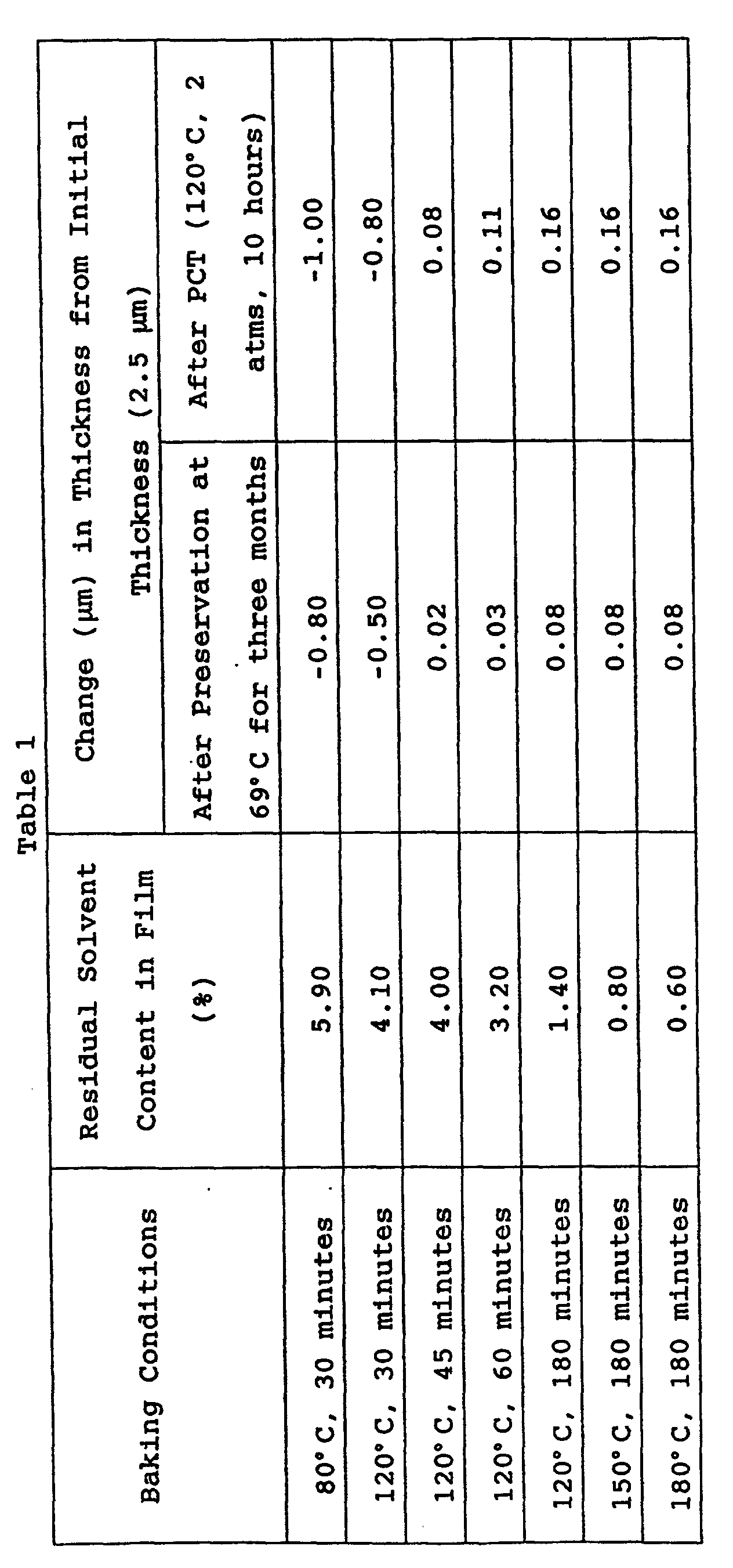
- the polyether amide protective layer 107 is generally formed by coating of a polyether amide solution, and the residual solvent content affects the ink resistance of the protective layer 107. According to results by the present inventors' research, a residual solvent content of 4% or less causes high resistance against the above-mentioned alkaline inks. In addition, a residual solvent content of 0.5% or less causes high resistance against the above-mentioned polar solvents.
- Such preferable residual solvent contents can be achieved by baking of the polyether amide film at a high temperature.
- the polyether amide film is baked at a temperature which is higher than the glass transition temperature (230°C) or more of the polyether amide, the layer has high resistance against both the alkaline inks and the polar solvents.
- a top board 108 having grooves is assembled on the protective layers so as to form ink channels 109 of the ink-jet substrate.
- the grooved top board 108 is formed by etching of glass or molding of a resin, such as polysulfone or polyether sulfone.
- the grooved top board 108 may be pressed onto the substrate using an elastic member not shown in the drawing, such as a presser bar spring to correct a warp formed during the molding. Since the polyether amide protective film 107 extends to the bonding sections to the grooved top board 108, the grooved top board 108 can be more firmly bonded to the substrate.
- a second protective layer composed of thallium is provided at bonding sections of a grooved top board, and the thallium has a Young's modulus of 1.90 ⁇ 10 4 kgf/cm 2 .
- the polyether amide used in the present invention has a Young's modulus of 260 kgf/cm 2 and is substantially the same as that of polysulfone which is generally used in the grooved top board 108.
- the polyether amide protective layer 107 is also deformed together with the grooved top board 108 by the pressing force to improve the bonding state.
- a single protective layer configuration may also be employed in the present invention.
- This embodiment shows an edge shooter-type configuration in which discharge nozzles (not shown in the drawing) are formed at the ends of the ink channels 109.
- the present invention is also applicable to a side-shooter type head having discharge nozzles provided above an exothermic element.
- a SiO 2 film having a thickness of 2.5 ⁇ m was formed on a Si wafer substrate by thermal oxidation.
- a 2.5- ⁇ m thick polyether amide film of HIMAL HL-1200 (Trade Name by Hitachi Chemical Co., Ltd.) was formed at the shaded section in Fig. 3 by the following steps.
- the substrate was cleaned and dried, and then a polyether amide solution (solvent: n-methyl-2-pyrrolidone) having a viscosity of 500 cP was coated onto the thermally oxidized SiO 2 film using a spinner.
- the solvent was preliminarily removed at 70°C for 30 minutes.
- the preliminarily dried substrate was baked under the conditions shown in Table 1 to prepare a plurality of samples.
- the residual solvent content in these films was determined by gas chromatography.
- a testing ink which was composed of 5 percent by weight of ethylene glycol, 5 percent by weight of urea, and the balance being water, a preservation test at 60°C and a pressure cooker test (PCT) were performed to observe the state of each film and a change in thickness of the film. The results are shown in Table 1.
- the polyether amide film in accordance with the present invention has high alkaline resistance, and particularly high resistance when the residual solvent content in the polyether amide film is 4.0% or less.
- a SiO 2 film having a thickness of 5 ⁇ m was formed on a 5-inch Si wafer substrate by thermal oxidation.
- a 2.5- ⁇ m thick polyether amide film of HIMAL HL-1200 (Trade Name by Hitachi Chemical Co.) was formed as in Experiment 1.
- the solvent was preliminarily removed at 70°C for 30 minutes.
- the preliminarily dried substrate was baked under the conditions shown in Table 2 to prepare Samples 1 to 5.
- the residual solvent content in these films was determined by gas chromatography. These films were immersed in ethyl cellosolve for 4 hours to observe the state of the film and to measure the change in the film thickness.
- Table 4 shows that the polyether amide films (Samples 4 and 5), which were baked at a temperature higher than the glass transition temperature (230°C) so as to control the residual solvent content to 0.5% or less, have high resistance against crack formation and dissolution in the polar ethyl cellosolve solvent. Samples 4 and 5 were subjected to the preservation test at 60°C and the PCT (120°C, 2 atm, 10 hr) using the testing ink as in Example 1. The film thickness was not decreased in the testing ink.
- An ink-jet head was prepared according to the following process and subjected to discharging tests.
- a 5-inch silicon wafer as a substrate 101 was thermally oxidized to form a 2.5- ⁇ m thick SiO 2 film as a heat-accumulating layer 102.
- a 0.15- ⁇ m thick exothermic element 103 composed of HfB 2 was formed on the heat-accumulating layer 102 by a sputtering process.
- a titanium (Ti) layer with a thickness of 0.005 ⁇ m and an aluminum (Al) layer with a thickness of 0.5 ⁇ m were continuously deposited thereon to form an electrode layer 104 by an electron beam deposition process.
- the electrode layer 104 was patterned by a photolithographic process, as shown in Figs. 1 and 2.
- the resulting heating zone 201 of the exothermic element 103 had a width of 30 ⁇ m, a length of 150 ⁇ m, and a resistance, including that of the aluminum electrode, of 150 ⁇ .
- Silicon oxide (SiO 2 ) was deposited on the entire substrate 101 to form a first protective layer 105 with a thickness of 2.2 ⁇ m.
- Thallium was deposited on the entire surface of the first protective layer 105 by a sputtering process and then patterned to form a second protective layer 106 with a thickness of 0.5 ⁇ m.
- a polyether amide layer 107 with a thickness of 2.5 ⁇ m was formed on the Ta second protective layer 106 by the following process.
- the substrate 101 having the second protective layer 106 was cleaned and dried.
- a polyether amide solution having a viscosity of 500 cP was coated onto the second protective layer 106 using a spinner. After drying it at 70°C for 30 minutes, the polyether amide layer was baked under the conditions shown in Table 3 to prepare Samples A, B and C.
- a novolak positive photoresist OFPR800 (Trade name by Tokyo Ohka Kogyo Co., Ltd.) with a thickness of 12 ⁇ m was coated on the polyether amide film using a spinner, and prebaked.
- the photoresist layer was exposed using a mask aligner, and developed to form a predetermined pattern.
- the substrate was placed into an oxygen plasma ashing system to ash the polyether amide.
- the ashing rate of the polyether amide was 0.2 ⁇ m/min without being affected by the baking conditions.
- the polyether amide with a thickness of 2.5 ⁇ m was ashed for 15 minutes in the oxygen plasma atmosphere.
- the substrate was immersed into a remover (Sipray 1112A), and the residual photoresist layer was removed by ultrasonic energy.
- the polyether amide film had a thickness of 2.5 ⁇ m after removal of the photoresist layer.
- the ashed section of the polyether amide film, near the thermal effect section, had a shape shown in Fig. 2 and a size of 50 ⁇ m ⁇ 250 ⁇ m.
- the wafer was cut into individual head substrates, and a glass top board 108 having grooves with a width of 50 ⁇ m, a depth of 50 ⁇ m and a length of 2 mm was bonded onto each of the cut substrates to form ink channels 109, as shown in Fig. 3.
- Pulses of 30-volts, 10- ⁇ sec, and 3-kHz were applied to the electrothermal transducers of the resulting ink-jet head. Droplets of the ink stored in the orifices were stably discharged in response to the applied signals. This operation was continued until the head did not discharge the ink droplets due to disconnection caused by electrolytic corrosion of the aluminum electrode and broken insulation between the protective layer and the aluminum electrode. The number of the repeated cycles was used as a measurement of durability.
- Table 3 shows that the heads in accordance with the present invention, that is, Samples B and C, in which the residual solvent content in the polyether amide film is 4.0 percent by weight or less, have high durability, that is, good printing quality after more than 10 9 repeated cycles.
- Sample A and the Photoneece sample electrolytic corrosion of the aluminum electrode due to immersion of the ink through pinholes in the SiO 2 or thallium sputtered layer is noticeable. Electrolytic corrosion of the Photoneece sample is particularly noticeable and thus deterioration of the quality of the print is significant.
- ink-jet heads for discharging tests were produced under a process disclosed in Japanese Patent Application Laid-Open No. 61-154947 in which a solid layer was provided on an ink channel pattern of a substrate, at least a part of a channel-forming member was provided thereon, and the solid layer was removed from the substrate.
- a polyether amide protective layer was formed on the substrate as in Experiment 2, a photoresist PMER P-AR900 (trade name by Tokyo Ohka Kogyo Co., Ltd.) with a thickness of 30 ⁇ m was applied onto the substrate, and patterned to form ink channels. The pattern was covered with an epoxy photo-curable resin.
- the epoxy resin was exposed at a dose of 8.5 J/cm 2 to be cured, and the substrate was cut using a dicing machine to form discharge nozzles.
- the PMER P-AR900 photoresist was removed in ethyl cellosolve as a polar solvent.
- Example 2 The resulting ink-jet heads were subjected to the continuous discharging tests as in Example 1. The results are shown in Table 4, wherein Samples 3 to 5 in Table 4 correspond to Samples 3 to 5 in Table 2, respectively.
- Table 4 demonstrates that Samples 4 and 5 having a residual solvent content in the polyether amide film of 0.5 percent by weight or less shows high print quality after more than 10 9 operation cycles.
- these ink-jet heads are suitable for a multiple head.
- the print quality of Sample 3 is significantly inferior to that of Samples 4 and 5 after 10 7 to 10 9 printing cycles, although no problem in durability occurs.
- electrolytic corrosion of the aluminum electrode due to immersion of the ink through pinholes in the SiO 2 or thallium sputtered layer is noticeable.
- a highly reliable multiple head can be produced by the process disclosed in Japanese Patent Application Laid-Open No. 61-154947, by baking the polyether amide at a temperature higher than the glass transition temperature thereof and by controlling the residual solvent content to 0.5% or less.
- a polyether amide protective layer was formed on each substrate 101 as in Experiment 2, and a polysulfone grooved top board 108 was precisely placed on the substrate 101 so that each exothermic element corresponds to an ink channel.
- the grooved top board 108 and the substrate 101 were fixed using a phosphor bronze presser bar spring 110.
- the polyamide film was patterned so as to extend to the section in contact with the top board. The print quality of these heads was high after discharge durability tests.
- each head has an edge shooter configuration in which ink is discharged substantially parallel to the exothermic element.
- the present invention is also applicable to a side shooter-type head.
- an inorganic insulating layer composed of SiN or SiO 2 and a thallium anti-cavitation layer are generally provided on the exothermic element to reduce damage due to cavitation caused by electrolytic corrosion of the ink and defoaming of the bubble. Since the thallium film has low bonding force to a resin as an ink channel component, detachment of the ink channel component from the thallium film will occur.
- a possible method for improving the bonding force is removal of the thallium film at the portion for providing the ink channel component.
- a resin is formed on the electrothermal transducer with only the inorganic insulating layer provided therebetween. Since the inorganic insulating layer is generally porous and permeates ions contained in the resin, these ions will cause electrolytic corrosion of the electrothermal transducer.
- the substrate may be subjected to treatment using a silane coupling agent or may be provided with an overlying resin layer composed of a polyimide (for example, Photoneece made by Toray Industries, Inc.) to improve the bonding force between the substrate having an ink-discharging force generating element and the ink channel component.
- a silane coupling agent for example, Photoneece made by Toray Industries, Inc.
- a polyether amide resin layer as the bottom layer of the substrate can maintain high bonding force for long periods even when an alkaline ink is used and even when the metal such as thallium is exposed on the bonding face, as described below.
- a polyether amide resin layer was provided between a substrate and a nozzle material and the bonding force was evaluated using a weakly alkaline ink by an accelerated test.
- the polyether amide resin layer is referred to as a bonding layer.
- a 5-inch silicon wafer was thermally oxidized to form a 1.0- ⁇ m SiO 2 layer.
- a N-methylpyrrolidone/butyl cellosolve acetate solution of a polyether amide resin HIMAL1200 made by Hitachi Chemical Co., Ltd. was coated thereon by a spin coating process, and heated at 100°C for 30 minutes and then at 250°C for one hour to form a bonding layer with a thickness of 1.5 ⁇ m.
- the heating of the thermoplastic polyether amide was performed to evaporate the solvents and to reduce internal stress at a temperature higher than the glass transition temperature (230°C).
- a dry film resist RISTON (trade name by DuPont) with a thickness of 20 ⁇ m was laminated on the substrate and patterned using a mask aligner PLA600 to form a line-and-space pattern with an interval of 30 ⁇ m.
- the substrate was heated at 150°C for one hour to completely cure the pattern.
- a sample not having a bonding layer and a sample having a 1.5- ⁇ m thick bonding layer composed of a polyimide Photoneece UR3100 made by Toray Industries, Inc. and baked at 400°C were also prepared for comparison.
- the pattern shape did not change after the PCT test.
- an interference fringe or separation were observed in a part of the pattern, probably due to insufficient bonding between the SiO 2 layer and the nozzle material.
- the polyimide layer disappeared by dissolution.
- the polyether amide bonding layer in accordance with the present invention has high bonding force and high ink resistance.
- the following is an example using a substrate having a SiN layer and a Ta layer and an epoxy resin nozzle material (ink channel component).
- a 1.0- ⁇ m thick SiN film and a 0.25- ⁇ m thick thallium film were formed on a 5-inch wafer as a substrate by a plasma enhanced CVD process.
- a polyether amide film was formed as in Experiment 3, and a solution of the following epoxy resin composition was applied on the polyether amide film and then patterned.
- This composition was patterned by cationic polymerization of the epoxy resin by light irradiation of a dose of 3.0 J/cm 2 using a mask aligner MPA600 made by Canon Kabusiki Kaisha, heated at 90°C for 30 minutes on a hot plate, developed in a methyl isobutyl ketone/xylene mixed solvent, and heated at 180°C for one hour to completely cure the resin.
- a line-and-space pattern with a thickness of 20 ⁇ m and an interval of 30 ⁇ m was thereby formed, as in Experiment 3.
- the sample was subjected to a PCT to observe a change in the line-and space pattern. No change in the pattern was observed in this sample having the polyether amide bonding layer in accordance with the present invention.
- an interference fringe and separation probably caused by insufficient bonding force between the Thallium layer and the nozzle material, were observed in a part of the pattern.
- An ink-jet head was prepared by the following procedure.
- a TaN electrothermal transducer 2 for generating pressure was formed on a silicon wafer substrate of a ⁇ 100> crystal axis having an ink nozzle mask 3. Also, a SiN layer 4 and a thallium layer 5 were formed as protective layers. The electrothermal transducer 2 was connected to electrodes for inputting control signals (not shown in the drawing).
- Fig. 6 is a cross-sectional view taken along line VI-VI in Fig. 5.
- a polyether amide bonding layer 6 with a thickness of 2.0 ⁇ m was formed on the substrate 1 as follows.
- the polyether amide used was HIMAL1200 made by Hitachi Chemical Co., Ltd.
- the polyether amide was coated on the substrate 1 using a spinner and baked at 100°C for 30 minutes and then at 250°C for one hour.
- a positive resist OFPR800 made by Tokyo Ohka Kogyo Co., Ltd. was patterned on the polyether amide, and then the polyether amide layer was patterned by oxygen plasma ashing through the resist mask. The resist mask was removed to form a bonding layer 6.
- an epoxy resin layer 8 was formed on the substrate 1, as in Experiment 4, and patterned to form discharge nozzles 9.
- the silicon substrate 1 was subjected to anisotropic etching to form an ink supply port 10.
- the SiN layer 4 above the ink supply port 10 and the ink channel pattern 7 were removed, and then the substrate was heated at 180°C for one hour to complete curing of the epoxy resin 8.
- the epoxy resin 8 as a nozzle component was bonded to the surface (thallium + SiN) of the substrate 1 with the bonding layer 6 provided therebetween.
- An ink-jet head without a bonding layer 6 was also prepared for comparison.
- the nozzle component 8 of the comparative ink-jet head was directly bonded to the surface (thallium + SiN) of the substrate 1.
- the substrate can be bonded to an ink channel component by the polyether amide film provided therebetween, as described in detail below.
- a 2.5- ⁇ m thick SiO 2 film as a heat-accumulating layer was formed on a 5-inch silicon wafer substrate by thermal oxidation.
- a 0.15- ⁇ m HfB 2 layer was formed on the silicon wafer substrate by a sputtering process to form an exothermic element.
- a 0.005- ⁇ m thick thallium layer and then a 0.5- ⁇ m thick aluminum layer were deposited thereon by an electron beam deposition process to form electrode layers.
- the electrode layers were patterned by a photolithographic process, as shown in Fig. 1.
- the heater 201 in Fig. 1 had a width of 30 ⁇ m, and a length of 150 ⁇ m.
- the resistance of the heater including the aluminum electrode was 150 ⁇ .
- SiO 2 with a thickness of 2.2 ⁇ m was deposited on the entire surface of the substrate by a sputtering process to form a first protective film.
- thallium with a thickness of 0.5 ⁇ m was deposited on the entire surface thereof by a sputtering process to form a second protective layer, and then patterned.
- a 3- ⁇ m thick polyether amide layer as a protective layer 107 was formed on the hatched portion in Fig. 1, as follows.
- the substrate 101 having the second protective layer 106 was cleaned and dried.
- a polyether amide (HIMAL) solution having a viscosity of 500 cP was coated onto the second protective layer 106 using a spinner. After drying it at 70°C for 30 minutes, the polyether amide layer was baked at 70°C for 3 hours.
- HIMAL polyether amide
- a novolak positive photoresist OFPR800 (Trade name by Tokyo Ohka Kogyo Co., Ltd.) with a thickness of 12 ⁇ m was coated on the polyether amide film using a spinner, and prebaked.
- the photoresist layer was exposed using a mask aligner, and developed to form a predetermined pattern.
- the substrate was placed into an oxygen plasma ashing system to ash the polyether amide.
- the ashing rate of the polyether amide was 0.2 ⁇ m/min without being affected by the baking conditions.
- the polyether amide with a thickness of 2.5 ⁇ m above the heater 201 was removed by ashing for 15 minutes in the oxygen plasma atmosphere.
- the substrate was immersed into a remover (Sipray 1112A), and the residual photoresist layer was removed by ultrasonic energy.
- the ashed section of the polyether amide film, near the thermal effect section, had a shape shown in Fig. 1 and a size of 50 ⁇ m ⁇ 250 ⁇ m.
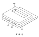
- a grooved top board was bonded to the upper face of the substrate.
- the grooved top board consisted of a glass board 500 and a polyether amide film 600 with a thickness of 50 ⁇ m formed thereon.
- the polyether amide film 600 was formed by two cycles of spin coating of a polyether amide (HIMAL) solution with a viscosity of 900 cP, drying at 70°C for 30 minutes, and then baking under the conditions A and B in Table 2.
- HIMAL polyether amide
- a resist was applied onto the other surface not having the polyether amide film 600 of the glass substrate 500, and patterned.
- the glass board 500 was patterned using an aqueous mixture of hydrofluoric acid and ammonium fluoride to form an ink supply port. After removing the resist, the top board was cut using a dicer. Ink channels 230 having a width of 50 ⁇ m, a depth of 40 ⁇ m. and a length of 2 ⁇ m were formed on the polyether amide film 600 by cutting.
- ink channels are formed by direct cutting of a glass plate in conventional technologies, cracking and chipping inevitably occur.
- the polyether amide layer 600 in accordance with the present invention can be cut without cracking or chipping.
- the substrate 430 was placed on a hot plate at 300°C, and the grooved top board 500 was placed and aligned on the substrate 430.
- the grooved top board 500 was pressed for 10 seconds using a heater at 300°C to weld the grooved top board 500 with the substrate 430.
- the polyether amide layer was also provided at the portion of the substrate 430 corresponding to bottom walls of nozzles to facilitate bonding of the top board 500 provided with the nozzles to the substrate 430.
- the polyether polyamide layer absorbs a large difference in level caused by wiring on the substrate 430, and thus can facilitate bonding of the grooved top board 400 to the substrate 430, although such bonding can be achieved by welding of the polyether amide layer coated on the top board 500 even when the substrate 430 does not have the polyether amide layer.
- Pulses of 30-volts, 10- sec, and 3-kHz were applied to the electrothermal transducers of the resulting ink-jet head. Droplets of the ink stored in the orifices were stably discharged in response to the applied signals. The quality of the print was satisfactory. The polyether amide layer did not cause problems, such as separation.
- a substrate 410 was produced as in Example 5.
- a polyether amide (HIMAL) solution having a viscosity of 900 cP was applied twice on the substrate 410 by a spin coating process, dried at 70°C for 30 minutes, and then baked at 120°C for 3 hours.
- the resulting polyether amide film had a thickness of 30 ⁇ m.
- a resist pattern was formed in the polyether amide film.
- An ink channel was formed by an oxygen plasma process, and then the resist pattern was removed.
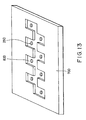
- etching resist PMERP-RF30S (trade name, by Tokyo Ohka Kogyo Co., Ltd.) was applied onto a copper plate, an ink channel 800 was patterned, and then the resist was removed.
- Discharge nozzles 250 were formed using a YAG (yttrium-aluminum-garnet) laser, and the surface of the copper plate was plated with gold. An orifice plate 700 was thereby formed.
- the substrate 410 and the orifice plate 700 were aligned and bonded to each other. These were placed onto a hot plate at 300°C, and then the orifice plate 700 was pressed for 10 seconds using a heater at 300°C to weld it with the substrate 410. An ink-jet head was thereby formed as shown in Fig. 14.
- Pulses of 30-volts, 10- sec, and 3-kHz were applied to the electrothermal transducers of the resulting ink-jet head.
- Droplets of the ink stored in the orifices were stably discharged in response to the applied signals, as in Example 5.
- the quality of the print was satisfactory.
- the polyether amide layer did not cause problems, such as separation.
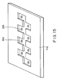
- a substrate was formed as in Example 5.
- a polyether amide (HIMAL) solution having a viscosity of 900 cP was applied twice on the substrate by a spin coating process, and dried at 70°C for 30 minutes.
- the substrate was bonded to a resin orifice plate 710 shown in Fig. 15 to form ink channels and discharge nozzles.
- An ink channel 810 was simultaneously formed with the orifice plate 710 by molding, and then discharge nozzles 255 were formed using an excimer laser.
- the substrate and the orifice plate 710 were aligned and bonded to each other. These were placed into a vacuum chamber and a load was added thereto at room temperature to evaporate a solvent, butyl cellosolve acetate, used for dissolution of the polyether amide.
- the present invention is capable of using an inexpensive resin orifice plate.
- Pulses of 30-volts, 10- sec, and 3-kHz were applied to the electrothermal transducers of the resulting ink-jet head.
- Droplets of the ink stored in the orifices were stably discharged in response to the applied signals, as in Example 5.
- the quality of the print was satisfactory.
- the polyether amide layer did not cause problems, such as separation.
Landscapes
- Engineering & Computer Science (AREA)
- Manufacturing & Machinery (AREA)
- Particle Formation And Scattering Control In Inkjet Printers (AREA)
Description
- The present invention relates to an ink-jet head for discharging liquid through an orifice and for forming droplets, an ink-jet head substrate, and a method for making the head.
- Japanese Patent Application Laid Open No. 54-51837 discloses an ink-jet recording process, which is different from other ink-jet recording processes. That is, thermal energy is applied to liquid. The heated liquid forms a bubble, and a force generated by the formation of the bubble discharges a droplet of the liquid through an orifice at the tip of an ink-jet head. The droplet adheres on a recording medium to record information.
- The ink-jet head used in this recording process has a liquid-discharging section having an orifice for discharging droplets and a liquid channel provided with a heating section for imparting thermal energy to the liquid, an exothermic element as an electrothermal transducer which generates pressure capable of discharging ink, electrodes for applying electrical energy, and a substrate for holding these components. The head has a heat-accumulating layer provided between the exothermic element and the substrate, and an upper protective layer for protecting the exothermic element and the electrodes from ink.
- Japanese Patent Application Laid-Open No. 59-194866 discloses an organic topmost layer formed on an upper protective layer, that is, a surface layer of the substrate. Tthe organic layer has small amounts of pinhole defects and has high coverage, although the layer does not have thermal resistance. Organic materials proposed as the surface layer of the substrate are silicone resins, fluorinated resins, polyamide resins, polyimide resins, epoxy resins, phenol resins, Zirox resins, triazine resins, and BT (bismaleimide-triazine) resins. Among these, polyimide resins are generally used since the resins can readily form films and have high ink resistance.
- In recent ink-jet processes, use of various types of paper, for example, plain paper, is required. Thus, inks used in these processes have inherent properties which are different from that of conventional inks. Such inks readily spread on plain paper to decrease the print density compared with coated paper. The dye content in the ink must be increased to enhance the print density. The ink having a high dye content prompts precipitation or adhesion of the dye at a nozzle tip. Thus, urea as a humectant is added to the ink having a high dye content so that the dye does not adhere.
- A head containing a urea-containing ink which is designed based on the above-described concept will break down after a long continuous operation. In the head, at failure, the polyimide resin layer on the substrate surface is lost. Thus, the polyimide resin is unsuitable for urea-containing inks. Accordingly, required organic resins must facilitate formation of films, and must have high resistance against urea-containing inks and thermal resistance.
- In addition, inks capable of recording on various media, other than plain paper, are desirable. Furthermore, alkaline inks will be developed in future, instead of conventional neutral inks. Thus, ink-jet recording systems must allow use of a wide variety of inks.
- Japanese Patent Application Laid-Open No. 61-154947 discloses a method for making an ink-jet head, in which a solid layer having a channel pattern is formed on a substrate, a material for forming a channel is provided thereon, and then the solid layer is removed. When a positive resist is used as the patterned solid layer and when an epoxy resin is used as the ink channel component, an aqueous inorganic or organic alkaline solution or a polar solvent is used to remove the positive resist. Use of a metallic material, such as aluminum, in the substrate and the top board has heat accumulation and material cost advantages compared to Si substrates. Such a metallic material may be dissolved in the aqueous inorganic or organic alkaline solution. Thus, use of a polar solvent such as ethyl cellosolve (ethylene glycol monoethyl ether) is preferable.
- Since organic polar solvents dissolve polymeric compounds not soluble in nonpolar solvents, the use of organic polar solvents in production of ink-jet heads will form cracks and voids in the organic layer on the substrate surface or will completely dissolve the organic layer. Accordingly, the material used as the surface layer of the substrate must have resistance against a solution for removing the positive resist, in addition to resistance against the alkaline ink.
- Accordingly, it is an object of the present invention to provide an ink-jet head substrate having a stable surface layer which is highly resistive against alkaline inks and polar solvents.
- It is another object of the present invention to provide an ink-jet head.
- It is still another object of the present invention to provide a method for making an ink-jet head.
- An aspect of the present invention is an ink-jet head substrate according to
claim 1. - Another aspect of the present invention is an ink-jet head according to
claim 2. - A third aspect of the present invention is a method for making an ink-jet head according to claim 15.
- In the ink-jet head, the liquid channel component may be a top board having a groove for forming a part of the liquid channel.
- The top board may be pressed and fixed to the substrate by an elastic member.
- The ink-jet head in accordance with the present invention may be of an edge shooter type and of a side shooter type.
-
- Fig. 1 is a plan view of an ink-jet head substrate in accordance with the present invention;
- Fig. 2 is a cross-sectional view taken along line II-II in Fig. 1;
- Fig. 3 is a cross-sectional view of an ink-jet head along the liquid channel;
- Fig. 4 is a schematic view of an ink-jet head of Example 3;
- Fig. 5 is an isometric view of an ink-jet head substrate of Example 4;
- Figs. 6 to 11 are cross-sectional views for illustrating a method for making an ink-jet head of Example 4;
- Fig. 12 is a schematic isometric view of an ink-jet head of Example 5;
- Fig. 13 is a schematic isometric view of an orifice plate of Example 6;
- Fig. 14 is a schematic isometric view of an ink-jet head of Example 6; and
- Fig. 15 is a schematic isometric view of an orifice plate of Example 7.
-
- Fig. 1 is a plan view of an ink-jet head substrate in accordance with the present invention, and Fig. 2 is a cross-sectional view taken along line II-II in Fig. 1. Fig. 3 is a cross-sectional view of an ink-jet head using the substrate shown in Fig. 1.
- With reference to Figs. 2 and 3, a
substrate 101 is generally composed of silicon, ceramic or metal. An electrothermal transducer consisting of anexothermic layer 103 andelectrode layers 104 is provided above thesubstrate 101. Theexothermic layer 103 is composed of, for example, TaN or HfB2, and theelectrode layers 104 are composed of, for example, aluminum. When a voltage is applied to the electrothermal transducer based on driving information, the portion of theexothermic element 201 not covered with theelectrode layers 104 is heated. A heat-accumulatinglayer 102 composed of SiO2 or the like is provided on thesubstrate 101 so as to effectively conduct the heat generated in theexothermic element 201 to ink. Thus, theexothermic element 201 is formed on the heat-accumulatinglayer 102. In this embodiment, threeprotective layers exothermic element 201 from electrolytic corrosion, although the number of the protective layers is not limited. The firstprotective layers 105 is composed of inorganic insulator such as SiO2 and the secondprotective layer 106 is composed of Ta or the like and functions as a cavitation resistant layer. Furthermore, the thirdprotective layer 107 composed of a polyether amide is provided in order to improve ink resistance of the firstprotective layer 105. It is preferable that the polyether amideprotective layer 107 be not provided right above theexothermic element 201 in view of thermal resistance, Thus, the polyether amide film is patterned as shown in Fig. 1. The patterning is preferably performed by any dry etching process. In particular, an oxygen plasma ashing process is suitable for highly precise patterning. The polyether amideprotective layer 107 is generally formed by coating of a polyether amide solution, and the residual solvent content affects the ink resistance of theprotective layer 107. According to results by the present inventors' research, a residual solvent content of 4% or less causes high resistance against the above-mentioned alkaline inks. In addition, a residual solvent content of 0.5% or less causes high resistance against the above-mentioned polar solvents. Such preferable residual solvent contents can be achieved by baking of the polyether amide film at a high temperature. When the polyether amide film is baked at a temperature which is higher than the glass transition temperature (230°C) or more of the polyether amide, the layer has high resistance against both the alkaline inks and the polar solvents. - With reference to Fig. 3, a
top board 108 having grooves is assembled on the protective layers so as to formink channels 109 of the ink-jet substrate. The groovedtop board 108 is formed by etching of glass or molding of a resin, such as polysulfone or polyether sulfone. When the groovedtop board 108 is formed by resin molding, the groovedtop board 108 may be pressed onto the substrate using an elastic member not shown in the drawing, such as a presser bar spring to correct a warp formed during the molding. Since the polyether amideprotective film 107 extends to the bonding sections to the groovedtop board 108, the groovedtop board 108 can be more firmly bonded to the substrate. In a conventional configuration, a second protective layer composed of thallium is provided at bonding sections of a grooved top board, and the thallium has a Young's modulus of 1.90×10⁴ kgf/cm2. In contrast, the polyether amide used in the present invention has a Young's modulus of 260 kgf/cm2 and is substantially the same as that of polysulfone which is generally used in the groovedtop board 108. The polyether amideprotective layer 107 is also deformed together with the groovedtop board 108 by the pressing force to improve the bonding state. Since this Young's modulus is lower than that (300 kgf/cm2) of a polyimide used in a conventional third protective layer, the bonding state in the present invention is improved compared to a configuration using a polyimide as the third protective layer. - A single protective layer configuration may also be employed in the present invention. This embodiment shows an edge shooter-type configuration in which discharge nozzles (not shown in the drawing) are formed at the ends of the
ink channels 109. The present invention is also applicable to a side-shooter type head having discharge nozzles provided above an exothermic element. - Experiments for investigating the ink resistance of the polyether amide film will now be described.
- A SiO2 film having a thickness of 2.5 µm was formed on a Si wafer substrate by thermal oxidation. A 2.5-µm thick polyether amide film of HIMAL HL-1200 (Trade Name by Hitachi Chemical Co., Ltd.) was formed at the shaded section in Fig. 3 by the following steps. The substrate was cleaned and dried, and then a polyether amide solution (solvent: n-methyl-2-pyrrolidone) having a viscosity of 500 cP was coated onto the thermally oxidized SiO2 film using a spinner. The solvent was preliminarily removed at 70°C for 30 minutes. The preliminarily dried substrate was baked under the conditions shown in Table 1 to prepare a plurality of samples. The residual solvent content in these films was determined by gas chromatography. Using a testing ink, which was composed of 5 percent by weight of ethylene glycol, 5 percent by weight of urea, and the balance being water, a preservation test at 60°C and a pressure cooker test (PCT) were performed to observe the state of each film and a change in thickness of the film. The results are shown in Table 1.
- As shown in Table 1, all the polyether films did not disappear after the preservation at 60°C for three months and after the PCT. For comparison, a 2.5-µm thick polyimide film of Photoneece (trade name, by Toray Industries, Inc.) was baked at 400°C and subjected to the preservation test at 60°C for three months and the TCT test. The Photoneece film disappeared after the preservation test. When the residual solvent content in the polyether amide film was 4.0% or less, no disappearance of the film was observed although the film was swelled by water in the tested ink.
- These results show the polyether amide film in accordance with the present invention has high alkaline resistance, and particularly high resistance when the residual solvent content in the polyether amide film is 4.0% or less.
- A SiO2 film having a thickness of 5 µm was formed on a 5-inch Si wafer substrate by thermal oxidation. A 2.5-µm thick polyether amide film of HIMAL HL-1200 (Trade Name by Hitachi Chemical Co.) was formed as in
Experiment 1. The solvent was preliminarily removed at 70°C for 30 minutes. The preliminarily dried substrate was baked under the conditions shown in Table 2 to prepareSamples 1 to 5. The residual solvent content in these films was determined by gas chromatography. These films were immersed in ethyl cellosolve for 4 hours to observe the state of the film and to measure the change in the film thickness. - Table 4 shows that the polyether amide films (
Samples 4 and 5), which were baked at a temperature higher than the glass transition temperature (230°C) so as to control the residual solvent content to 0.5% or less, have high resistance against crack formation and dissolution in the polar ethyl cellosolve solvent.Samples 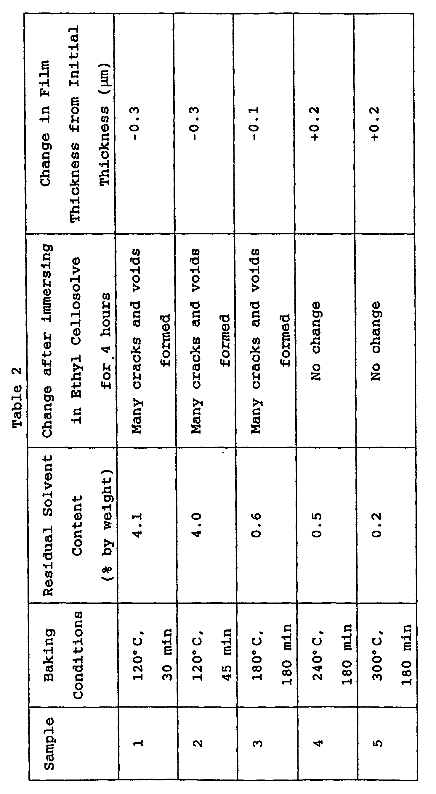
- An ink-jet head was prepared according to the following process and subjected to discharging tests.
- As shown Figs. 1 and 2, a 5-inch silicon wafer as a
substrate 101 was thermally oxidized to form a 2.5-µm thick SiO2 film as a heat-accumulatinglayer 102. A 0.15-µm thickexothermic element 103 composed of HfB2 was formed on the heat-accumulatinglayer 102 by a sputtering process. Then, a titanium (Ti) layer with a thickness of 0.005 µm and an aluminum (Al) layer with a thickness of 0.5 µm were continuously deposited thereon to form anelectrode layer 104 by an electron beam deposition process. Theelectrode layer 104 was patterned by a photolithographic process, as shown in Figs. 1 and 2. The resultingheating zone 201 of theexothermic element 103 had a width of 30 µm, a length of 150 µm, and a resistance, including that of the aluminum electrode, of 150 Ω. - Silicon oxide (SiO2) was deposited on the
entire substrate 101 to form a firstprotective layer 105 with a thickness of 2.2 µm. Thallium was deposited on the entire surface of the firstprotective layer 105 by a sputtering process and then patterned to form a secondprotective layer 106 with a thickness of 0.5 µm. - As as shown by the hatching pattern in Figs. 1 and 2, a
polyether amide layer 107 with a thickness of 2.5 µm was formed on the Ta secondprotective layer 106 by the following process. - The
substrate 101 having the secondprotective layer 106 was cleaned and dried. A polyether amide solution having a viscosity of 500 cP was coated onto the secondprotective layer 106 using a spinner. After drying it at 70°C for 30 minutes, the polyether amide layer was baked under the conditions shown in Table 3 to prepare Samples A, B and C. - After the baking, a novolak positive photoresist OFPR800 (Trade name by Tokyo Ohka Kogyo Co., Ltd.) with a thickness of 12 µm was coated on the polyether amide film using a spinner, and prebaked. The photoresist layer was exposed using a mask aligner, and developed to form a predetermined pattern. The substrate was placed into an oxygen plasma ashing system to ash the polyether amide. The ashing rate of the polyether amide was 0.2 µm/min without being affected by the baking conditions. The polyether amide with a thickness of 2.5 µm was ashed for 15 minutes in the oxygen plasma atmosphere. Next, the substrate was immersed into a remover (Sipray 1112A), and the residual photoresist layer was removed by ultrasonic energy. The polyether amide film had a thickness of 2.5 µm after removal of the photoresist layer. The ashed section of the polyether amide film, near the thermal effect section, had a shape shown in Fig. 2 and a size of 50 µm × 250 µm.
- The wafer was cut into individual head substrates, and a
glass top board 108 having grooves with a width of 50 µm, a depth of 50 µm and a length of 2 mm was bonded onto each of the cut substrates to formink channels 109, as shown in Fig. 3. - Pulses of 30-volts, 10-µsec, and 3-kHz were applied to the electrothermal transducers of the resulting ink-jet head. Droplets of the ink stored in the orifices were stably discharged in response to the applied signals. This operation was continued until the head did not discharge the ink droplets due to disconnection caused by electrolytic corrosion of the aluminum electrode and broken insulation between the protective layer and the aluminum electrode. The number of the repeated cycles was used as a measurement of durability.
- Durability was compared using three polyether amide samples (Samples A, B and C) baked under different conditions and a Photoneece (polyimide) sample. The results are shown in Table 3.

- Table 3 shows that the heads in accordance with the present invention, that is, Samples B and C, in which the residual solvent content in the polyether amide film is 4.0 percent by weight or less, have high durability, that is, good printing quality after more than 109 repeated cycles. In contrast, in Sample A and the Photoneece sample, electrolytic corrosion of the aluminum electrode due to immersion of the ink through pinholes in the SiO2 or thallium sputtered layer is noticeable. Electrolytic corrosion of the Photoneece sample is particularly noticeable and thus deterioration of the quality of the print is significant.
- Using a polyether amide film formed under the baking conditions for
Samples 3 to 5 inExperiment 2, ink-jet heads for discharging tests were produced under a process disclosed in Japanese Patent Application Laid-Open No. 61-154947 in which a solid layer was provided on an ink channel pattern of a substrate, at least a part of a channel-forming member was provided thereon, and the solid layer was removed from the substrate. A polyether amide protective layer was formed on the substrate as inExperiment 2, a photoresist PMER P-AR900 (trade name by Tokyo Ohka Kogyo Co., Ltd.) with a thickness of 30 µm was applied onto the substrate, and patterned to form ink channels. The pattern was covered with an epoxy photo-curable resin. The epoxy resin was exposed at a dose of 8.5 J/cm2 to be cured, and the substrate was cut using a dicing machine to form discharge nozzles. The PMER P-AR900 photoresist was removed in ethyl cellosolve as a polar solvent. - The resulting ink-jet heads were subjected to the continuous discharging tests as in Example 1. The results are shown in Table 4, wherein
Samples 3 to 5 in Table 4 correspond toSamples 3 to 5 in Table 2, respectively. - Table 4 demonstrates that
Samples Sample 3 is significantly inferior to that ofSamples 
- Accordingly, a highly reliable multiple head can be produced by the process disclosed in Japanese Patent Application Laid-Open No. 61-154947, by baking the polyether amide at a temperature higher than the glass transition temperature thereof and by controlling the residual solvent content to 0.5% or less.
- Two ink-jet heads were produced using ink-jet head substrates having polyether amide films formed under the baking conditions for
Samples Experiment 2 by the following process, and subjected to discharging tests. - With reference to Fig. 4, a polyether amide protective layer was formed on each
substrate 101 as inExperiment 2, and a polysulfone groovedtop board 108 was precisely placed on thesubstrate 101 so that each exothermic element corresponds to an ink channel. The groovedtop board 108 and thesubstrate 101 were fixed using a phosphor bronzepresser bar spring 110. The polyamide film was patterned so as to extend to the section in contact with the top board. The print quality of these heads was high after discharge durability tests. - In the above-mentioned examples, each head has an edge shooter configuration in which ink is discharged substantially parallel to the exothermic element. The present invention is also applicable to a side shooter-type head.
- In a bubble-jet head for generating an ink discharging force using an exothermic element, forming a bubble by membrane boiling of ink to discharge the ink, an inorganic insulating layer composed of SiN or SiO2 and a thallium anti-cavitation layer are generally provided on the exothermic element to reduce damage due to cavitation caused by electrolytic corrosion of the ink and defoaming of the bubble. Since the thallium film has low bonding force to a resin as an ink channel component, detachment of the ink channel component from the thallium film will occur.
- A possible method for improving the bonding force is removal of the thallium film at the portion for providing the ink channel component. In such a case, a resin is formed on the electrothermal transducer with only the inorganic insulating layer provided therebetween. Since the inorganic insulating layer is generally porous and permeates ions contained in the resin, these ions will cause electrolytic corrosion of the electrothermal transducer.
- The substrate may be subjected to treatment using a silane coupling agent or may be provided with an overlying resin layer composed of a polyimide (for example, Photoneece made by Toray Industries, Inc.) to improve the bonding force between the substrate having an ink-discharging force generating element and the ink channel component.
- Separation between the substrate and the ink channel component caused by ink must be avoided during operation under ordinary conditions. Weakly alkaline inks, which have been recently used due to the required use of a variety of recording sheets and water resistance of inks, will decrease the bonding force between the substrate and the ink channel component during long-term use.
- A polyether amide resin layer as the bottom layer of the substrate can maintain high bonding force for long periods even when an alkaline ink is used and even when the metal such as thallium is exposed on the bonding face, as described below.
- A polyether amide resin layer was provided between a substrate and a nozzle material and the bonding force was evaluated using a weakly alkaline ink by an accelerated test. Hereinafter, the polyether amide resin layer is referred to as a bonding layer.
- A 5-inch silicon wafer was thermally oxidized to form a 1.0-µm SiO2 layer. A N-methylpyrrolidone/butyl cellosolve acetate solution of a polyether amide resin HIMAL1200 made by Hitachi Chemical Co., Ltd. was coated thereon by a spin coating process, and heated at 100°C for 30 minutes and then at 250°C for one hour to form a bonding layer with a thickness of 1.5 µm. The heating of the thermoplastic polyether amide was performed to evaporate the solvents and to reduce internal stress at a temperature higher than the glass transition temperature (230°C).
- A dry film resist RISTON (trade name by DuPont) with a thickness of 20 µm was laminated on the substrate and patterned using a mask aligner PLA600 to form a line-and-space pattern with an interval of 30µm. The substrate was heated at 150°C for one hour to completely cure the pattern.
- A sample not having a bonding layer and a sample having a 1.5-µm thick bonding layer composed of a polyimide Photoneece UR3100 made by Toray Industries, Inc. and baked at 400°C were also prepared for comparison.
- These samples were immersed into an ink composed of ethylene glycol/urea/isopropyl alcohol/black pigment/water = 5/3/2/3/87 parts by weight and then were subjected to PCT at 120°C in 2 atm for 50 hours to observe a change in the line-and space pattern. The ink contained urea as a humectant for suppressing evaporation of the ink and preventing clogging in the nozzle, and was weakly alkaline due to hydrolysis of the urea.
- In the sample having the polyether amide bonding layer in accordance with the present invention, the pattern shape did not change after the PCT test. In contrast, in the sample not having the bonding layer, an interference fringe or separation were observed in a part of the pattern, probably due to insufficient bonding between the SiO2 layer and the nozzle material. In the sample having the polyimide bonding layer, the polyimide layer disappeared by dissolution.
- Accordingly, the polyether amide bonding layer in accordance with the present invention has high bonding force and high ink resistance.
- The following is an example using a substrate having a SiN layer and a Ta layer and an epoxy resin nozzle material (ink channel component). A 1.0-µm thick SiN film and a 0.25-µm thick thallium film were formed on a 5-inch wafer as a substrate by a plasma enhanced CVD process. A polyether amide film was formed as in
Experiment 3, and a solution of the following epoxy resin composition was applied on the polyether amide film and then patterned. - Epoxy resin EHPE (trade name by Diacel Chemical Industries, Ltd.) 100 parts by weight
- Resin 1.4-HFAB (trade name by Central Glass Co., Ltd.) 20 parts by weight
- Silane coupling agent A-187 (trade name by Union Carbide Japan KK) 5 parts by weight
- Optical cationic polymerization catalyst SP170 (trade name by Asahi Denka Kogyo K.K.) 2 parts by weight
- This composition was patterned by cationic polymerization of the epoxy resin by light irradiation of a dose of 3.0 J/cm2 using a mask aligner MPA600 made by Canon Kabusiki Kaisha, heated at 90°C for 30 minutes on a hot plate, developed in a methyl isobutyl ketone/xylene mixed solvent, and heated at 180°C for one hour to completely cure the resin. A line-and-space pattern with a thickness of 20 µm and an interval of 30 µm was thereby formed, as in
Experiment 3. The sample was subjected to a PCT to observe a change in the line-and space pattern. No change in the pattern was observed in this sample having the polyether amide bonding layer in accordance with the present invention. In contrast, in a sample not having a bonding layer, an interference fringe and separation, probably caused by insufficient bonding force between the Thallium layer and the nozzle material, were observed in a part of the pattern. - An ink-jet head was prepared by the following procedure.
- With reference to Fig. 5, a TaN
electrothermal transducer 2 for generating pressure was formed on a silicon wafer substrate of a <100> crystal axis having anink nozzle mask 3. Also, aSiN layer 4 and athallium layer 5 were formed as protective layers. Theelectrothermal transducer 2 was connected to electrodes for inputting control signals (not shown in the drawing). Fig. 6 is a cross-sectional view taken along line VI-VI in Fig. 5. - With reference to Fig. 7, a polyether
amide bonding layer 6 with a thickness of 2.0 µm was formed on thesubstrate 1 as follows. The polyether amide used was HIMAL1200 made by Hitachi Chemical Co., Ltd. The polyether amide was coated on thesubstrate 1 using a spinner and baked at 100°C for 30 minutes and then at 250°C for one hour. - A positive resist OFPR800 made by Tokyo Ohka Kogyo Co., Ltd. was patterned on the polyether amide, and then the polyether amide layer was patterned by oxygen plasma ashing through the resist mask. The resist mask was removed to form a
bonding layer 6. - With reference to Fig. 8, an
ink channel pattern 7 with a thickness of 12 µm composed of a positive resist ODUR made by Tokyo Ohka Kogyo Co., Ltd. was formed on thesubstrate 1. - With reference to Fig. 9, an
epoxy resin layer 8 was formed on thesubstrate 1, as inExperiment 4, and patterned to formdischarge nozzles 9. - With reference to Fig. 10, the
silicon substrate 1 was subjected to anisotropic etching to form anink supply port 10. - With reference to Fig. 11, the
SiN layer 4 above theink supply port 10 and theink channel pattern 7 were removed, and then the substrate was heated at 180°C for one hour to complete curing of theepoxy resin 8. Theepoxy resin 8 as a nozzle component was bonded to the surface (thallium + SiN) of thesubstrate 1 with thebonding layer 6 provided therebetween. - An ink-jet head without a
bonding layer 6 was also prepared for comparison. Thus, thenozzle component 8 of the comparative ink-jet head was directly bonded to the surface (thallium + SiN) of thesubstrate 1. - These ink-jet heads filled with the ink described in
Experiment 3 were subjected to preservation tests at 60°C for three months. The ink-jet head of this example having the bonding layer did not show an interference fringe and separation at the bonded interface of the nozzle component. In contrast, the comparative ink-jet head without a bonding layer formed a partial interference fringe between the thallium layer and the nozzle component. Accordingly, the polyether amide bonding layer in accordance with the present invention has high bonding strength in an ink-jet head which can be used in practice. - When a polyether amide film is used as the surface layer of a substrate, the substrate can be bonded to an ink channel component by the polyether amide film provided therebetween, as described in detail below.
- A 2.5-µm thick SiO2 film as a heat-accumulating layer was formed on a 5-inch silicon wafer substrate by thermal oxidation. A 0.15-µm HfB2 layer was formed on the silicon wafer substrate by a sputtering process to form an exothermic element. A 0.005-µm thick thallium layer and then a 0.5-µm thick aluminum layer were deposited thereon by an electron beam deposition process to form electrode layers. The electrode layers were patterned by a photolithographic process, as shown in Fig. 1. The
heater 201 in Fig. 1 had a width of 30 µm, and a length of 150 µm. The resistance of the heater including the aluminum electrode was 150 Ω. - SiO2 with a thickness of 2.2 µm was deposited on the entire surface of the substrate by a sputtering process to form a first protective film. Next, thallium with a thickness of 0.5 µm was deposited on the entire surface thereof by a sputtering process to form a second protective layer, and then patterned.
- Next, a 3-µm thick polyether amide layer as a
protective layer 107 was formed on the hatched portion in Fig. 1, as follows. Thesubstrate 101 having the secondprotective layer 106 was cleaned and dried. A polyether amide (HIMAL) solution having a viscosity of 500 cP was coated onto the secondprotective layer 106 using a spinner. After drying it at 70°C for 30 minutes, the polyether amide layer was baked at 70°C for 3 hours. - After the baking, a novolak positive photoresist OFPR800 (Trade name by Tokyo Ohka Kogyo Co., Ltd.) with a thickness of 12 µm was coated on the polyether amide film using a spinner, and prebaked. The photoresist layer was exposed using a mask aligner, and developed to form a predetermined pattern. The substrate was placed into an oxygen plasma ashing system to ash the polyether amide. The ashing rate of the polyether amide was 0.2 µm/min without being affected by the baking conditions. The polyether amide with a thickness of 2.5 µm above the
heater 201 was removed by ashing for 15 minutes in the oxygen plasma atmosphere. Next, the substrate was immersed into a remover (Sipray 1112A), and the residual photoresist layer was removed by ultrasonic energy. The ashed section of the polyether amide film, near the thermal effect section, had a shape shown in Fig. 1 and a size of 50 µm × 250 µm. - With reference to Fig. 12, a grooved top board was bonded to the upper face of the substrate. The grooved top board consisted of a
glass board 500 and apolyether amide film 600 with a thickness of 50 µm formed thereon. Thepolyether amide film 600 was formed by two cycles of spin coating of a polyether amide (HIMAL) solution with a viscosity of 900 cP, drying at 70°C for 30 minutes, and then baking under the conditions A and B in Table 2. - A resist was applied onto the other surface not having the
polyether amide film 600 of theglass substrate 500, and patterned. Theglass board 500 was patterned using an aqueous mixture of hydrofluoric acid and ammonium fluoride to form an ink supply port. After removing the resist, the top board was cut using a dicer.Ink channels 230 having a width of 50 µm, a depth of 40 µm. and a length of 2 µm were formed on thepolyether amide film 600 by cutting. - Since ink channels are formed by direct cutting of a glass plate in conventional technologies, cracking and chipping inevitably occur. The
polyether amide layer 600 in accordance with the present invention, however, can be cut without cracking or chipping. - The
substrate 430 was placed on a hot plate at 300°C, and the groovedtop board 500 was placed and aligned on thesubstrate 430. The groovedtop board 500 was pressed for 10 seconds using a heater at 300°C to weld the groovedtop board 500 with thesubstrate 430. - In this example, the polyether amide layer was also provided at the portion of the
substrate 430 corresponding to bottom walls of nozzles to facilitate bonding of thetop board 500 provided with the nozzles to thesubstrate 430. The polyether polyamide layer absorbs a large difference in level caused by wiring on thesubstrate 430, and thus can facilitate bonding of the grooved top board 400 to thesubstrate 430, although such bonding can be achieved by welding of the polyether amide layer coated on thetop board 500 even when thesubstrate 430 does not have the polyether amide layer. - Pulses of 30-volts, 10- sec, and 3-kHz were applied to the electrothermal transducers of the resulting ink-jet head. Droplets of the ink stored in the orifices were stably discharged in response to the applied signals. The quality of the print was satisfactory. The polyether amide layer did not cause problems, such as separation.
- With reference to Figs. 13 and 14, a
substrate 410 was produced as in Example 5. A polyether amide (HIMAL) solution having a viscosity of 900 cP was applied twice on thesubstrate 410 by a spin coating process, dried at 70°C for 30 minutes, and then baked at 120°C for 3 hours. The resulting polyether amide film had a thickness of 30 µm. A resist pattern was formed in the polyether amide film. An ink channel was formed by an oxygen plasma process, and then the resist pattern was removed. - An etching resist PMERP-RF30S (trade name, by Tokyo Ohka Kogyo Co., Ltd.) was applied onto a copper plate, an
ink channel 800 was patterned, and then the resist was removed.Discharge nozzles 250 were formed using a YAG (yttrium-aluminum-garnet) laser, and the surface of the copper plate was plated with gold. Anorifice plate 700 was thereby formed. - The
substrate 410 and theorifice plate 700 were aligned and bonded to each other. These were placed onto a hot plate at 300°C, and then theorifice plate 700 was pressed for 10 seconds using a heater at 300°C to weld it with thesubstrate 410. An ink-jet head was thereby formed as shown in Fig. 14. - Pulses of 30-volts, 10- sec, and 3-kHz were applied to the electrothermal transducers of the resulting ink-jet head. Droplets of the ink stored in the orifices were stably discharged in response to the applied signals, as in Example 5. The quality of the print was satisfactory. The polyether amide layer did not cause problems, such as separation.
- A substrate was formed as in Example 5. A polyether amide (HIMAL) solution having a viscosity of 900 cP was applied twice on the substrate by a spin coating process, and dried at 70°C for 30 minutes. The substrate was bonded to a
resin orifice plate 710 shown in Fig. 15 to form ink channels and discharge nozzles. Anink channel 810 was simultaneously formed with theorifice plate 710 by molding, and then dischargenozzles 255 were formed using an excimer laser. - The substrate and the
orifice plate 710 were aligned and bonded to each other. These were placed into a vacuum chamber and a load was added thereto at room temperature to evaporate a solvent, butyl cellosolve acetate, used for dissolution of the polyether amide. - Since heat was not applied for bonding of the orifice plate to the substrate, these can be tightly bonded to each other without the adverse affect of heat, such as deformation of the ink channel and discharge nozzles. Thus, the present invention is capable of using an inexpensive resin orifice plate.
- Pulses of 30-volts, 10- sec, and 3-kHz were applied to the electrothermal transducers of the resulting ink-jet head. Droplets of the ink stored in the orifices were stably discharged in response to the applied signals, as in Example 5. The quality of the print was satisfactory. The polyether amide layer did not cause problems, such as separation.
- While the present invention has been described with reference to what are presently considered to be the preferred embodiments, it is to be understood that the invention is not limited to the disclosed embodiments. On the contrary, the invention is intended to cover various modifications and equivalent arrangements included within the scope of the appended claims.
Claims (19)
- An ink-jet head substrate comprising:wherein said protective layer is a resin layer comprising a polyether amide having a residual solvent content of 4% or less and said protective layer being formed on the surface of the substrate.a substrate layer (101),an electrothermal transducer (103) formed on the substrate layer for generating thermal energy, said electrothermal transducer having a thermal effect section (201) for applying thermal energy to liquid to form a bubble in the liquid;a nozzle (109), the thermal effect section being connected with the nozzle for discharging the liquid;a pair of electrodes (104) provided on the electrothermal transducer; anda protective layer provided on the electrothermal transducer,
- An ink-jet head comprising:wherein the substrate has a protective resin layer comprising a polyether amide resin at the bonded section to the liquid channel component and the residual solvent content of said polyether amide resin in 4% or less.a nozzle for discharging liquid;a liquid channel connected with the nozzle;a substrate having a pressure-generating element for discharging the liquid, the liquid channel including the pressure-generating element; anda liquid channel component bonded to the substrate to form the liquid channel;
- An ink-jet according to claim 2, wherein the polyether amid resin is thermoplastic.
- An ink-jet head according to claim 2, wherein the liquid channel component comprises a resin.
- An ink-jet according to claim 4, wherein the liquid channel component is formed of a cationic polymerization compound of an epoxy resin.
- An ink-jet head according to claim 2, wherein the liquid channel component is a top board having a groove for forming a part of the liquid channel.
- An ink-jet head according to claim 6, wherein the top board is pressed and fixed to the substrate by an elastic member.
- An ink-jet head according to claim 7, wherein the top board is formed by integral molding of a resin.
- An ink-jet head according to claim 8, wherein the top board comprises a polysulfone or polyether sulfone.
- An ink-jet head according to claim 2, wherein the nozzle is provided at a side away from the pressure-generating element.
- An ink-jet head according to claim 2, wherein the pressure-generating element is an electrothermal transducer.
- An ink-jet head according to claim 2, wherein the resin layer functions as a protective layer for the pressure-generating element.
- An ink-jet head according to claim 2, wherein the liquid channel component and the substrate are bonded to each other by heat welding of the resin layer.
- An ink-jet head according to claim 2, wherein the liquid channel component and the substrate are bonded to each other by vacuum drying of the resin layer.
- A method for making an ink-jet head comprising a nozzle for discharging liquid, a liquid channel connected with the nozzle, a substrate having a pressure-generating element for discharging the liquid, the liquid channel including the pressure-generating element, and a liquid channel component bonded to the substrate to form the liquid channel, the method comprising the steps of:forming a polyether amide layer on the pressure-generating element of the substrate wherein the polyether amide layer is baked to obtain a solvent content in the polyether amide layer of 4% or less;forming a liquid channel pattern on the polyether amide layer using a soluble resin;forming a covering resin layer for forming a liquid channel wall on the liquid channel pattern;forming the nozzle in the covering resin layer above the pressure-generating element; anddissolving the liquid channel pattern.
- A method for making an ink-jet head according to claim 15, further comprising the step of patterning the polyether amide layer by an oxygen plasma ashing process.
- A method for making an ink-jet head according to claim 15, wherein the polyether amide resin is thermoplastic.
- A method for making an ink-jet head according to claim 15, wherein the covering resin layer is formed of a cationic polymerization compound of an epoxy resin.
- A method for making an ink-jet head according to claim 15, wherein the pressure-generating element is an electrothermal transducer.
Applications Claiming Priority (6)
| Application Number | Priority Date | Filing Date | Title |
|---|---|---|---|
| JP15438998 | 1998-06-03 | ||
| JP15439098 | 1998-06-03 | ||
| JP15439198 | 1998-06-03 | ||
| JP15438998A JPH11348288A (en) | 1998-06-03 | 1998-06-03 | Substrate for inkjet head and inkjet head |
| JP15439098A JP4146932B2 (en) | 1998-06-03 | 1998-06-03 | Inkjet head |
| JP15439198A JP4146933B2 (en) | 1998-06-03 | 1998-06-03 | Ink jet head and method of manufacturing ink jet head |
Publications (2)
| Publication Number | Publication Date |
|---|---|
| EP0962320A1 EP0962320A1 (en) | 1999-12-08 |
| EP0962320B1 true EP0962320B1 (en) | 2005-01-05 |
Family
ID=27320655
Family Applications (1)
| Application Number | Title | Priority Date | Filing Date |
|---|---|---|---|
| EP99110640A Expired - Lifetime EP0962320B1 (en) | 1998-06-03 | 1999-06-02 | Ink-Jet head, ink-jet head substrate, and a method for making the head |
Country Status (4)
| Country | Link |
|---|---|
| US (1) | US6390606B1 (en) |
| EP (1) | EP0962320B1 (en) |
| DE (1) | DE69923033T2 (en) |
| ES (1) | ES2232047T3 (en) |
Families Citing this family (34)
| Publication number | Priority date | Publication date | Assignee | Title |
|---|---|---|---|---|
| US6379571B1 (en) * | 1998-06-11 | 2002-04-30 | Canon Kabushiki Kaisha | Etching method for processing substrate, dry etching method for polyetheramide resin layer, production method of ink-jet printing head, ink-jet head and ink-jet printing apparatus |
| KR100325521B1 (en) * | 1998-12-10 | 2002-04-17 | 윤종용 | Method for manufacturing fluid injector and fluid injector manufactured thereby |
| US6701921B2 (en) * | 2000-12-22 | 2004-03-09 | Chrysalis Technologies Incorporated | Aerosol generator having heater in multilayered composite and method of use thereof |
| JP3728210B2 (en) * | 2001-02-23 | 2005-12-21 | キヤノン株式会社 | Ink jet head, manufacturing method thereof, and ink jet recording apparatus |
| JP4054583B2 (en) | 2001-02-28 | 2008-02-27 | キヤノン株式会社 | Inkjet printhead manufacturing method |
| US6627467B2 (en) * | 2001-10-31 | 2003-09-30 | Hewlett-Packard Development Company, Lp. | Fluid ejection device fabrication |
| CN100581824C (en) | 2003-02-13 | 2010-01-20 | 佳能株式会社 | Manufacturing method of substrate for inkjet recording head |
| JP3963456B2 (en) * | 2003-06-16 | 2007-08-22 | キヤノン株式会社 | Photosensitive resin composition, ink jet recording head using the same, and method for producing the same |
| JP4455282B2 (en) * | 2003-11-28 | 2010-04-21 | キヤノン株式会社 | Inkjet head manufacturing method, inkjet head, and inkjet cartridge |
| US7325309B2 (en) * | 2004-06-08 | 2008-02-05 | Hewlett-Packard Development Company, L.P. | Method of manufacturing a fluid ejection device with a dry-film photo-resist layer |
| KR100612326B1 (en) * | 2004-07-16 | 2006-08-16 | 삼성전자주식회사 | Manufacturing method of inkjet head |
| JP2006126116A (en) * | 2004-11-01 | 2006-05-18 | Canon Inc | Filter substrate manufacturing method, ink jet recording head, and manufacturing method thereof |
| JP4241605B2 (en) * | 2004-12-21 | 2009-03-18 | ソニー株式会社 | Method for manufacturing liquid discharge head |
| JP4881081B2 (en) * | 2005-07-25 | 2012-02-22 | キヤノン株式会社 | Method for manufacturing liquid discharge head |
| US7523553B2 (en) * | 2006-02-02 | 2009-04-28 | Canon Kabushiki Kaisha | Method of manufacturing ink jet recording head |
| US7695111B2 (en) * | 2006-03-08 | 2010-04-13 | Canon Kabushiki Kaisha | Liquid discharge head and manufacturing method therefor |
| US8037603B2 (en) * | 2006-04-27 | 2011-10-18 | Canon Kabushiki Kaisha | Ink jet head and producing method therefor |
| US7550252B2 (en) * | 2006-09-21 | 2009-06-23 | Canon Kabushiki Kaisha | Ink-jet recording head and method for producing same |
| US8267503B2 (en) * | 2006-10-16 | 2012-09-18 | Canon Kabushiki Kaisha | Ink jet recording head and manufacturing method therefor |
| JP4953930B2 (en) * | 2007-06-13 | 2012-06-13 | キヤノン株式会社 | Ink jet recording head and manufacturing method thereof |
| JP4979641B2 (en) * | 2007-06-20 | 2012-07-18 | キヤノン株式会社 | Method for manufacturing liquid discharge head |
| JP5305691B2 (en) * | 2008-02-27 | 2013-10-02 | キヤノン株式会社 | Liquid discharge head and manufacturing method thereof |
| JP5147551B2 (en) * | 2008-06-05 | 2013-02-20 | キヤノン株式会社 | Manufacturing method of liquid discharge recording head |
| JP2010000632A (en) | 2008-06-18 | 2010-01-07 | Canon Inc | Substrate for inkjet head, and inkjet head equipped with substrate |
| US8291576B2 (en) * | 2008-06-18 | 2012-10-23 | Canon Kabushiki Kaisha | Method of manufacturing liquid ejection head |
| JP5388817B2 (en) * | 2008-12-12 | 2014-01-15 | キヤノン株式会社 | Method for manufacturing liquid discharge head |
| JP5328608B2 (en) * | 2008-12-15 | 2013-10-30 | キヤノン株式会社 | Substrate for liquid discharge head, liquid discharge head and manufacturing method thereof |
| US8286350B2 (en) * | 2009-02-25 | 2012-10-16 | Canon Kabushiki Kaisha | Method of manufacturing a liquid discharge head |
| KR20110032253A (en) * | 2009-09-22 | 2011-03-30 | 삼성전자주식회사 | Inkjet Printheads and Manufacturing Method Thereof |
| JP6083986B2 (en) | 2012-04-27 | 2017-02-22 | キヤノン株式会社 | Liquid discharge head |
| JP2014028471A (en) * | 2012-07-31 | 2014-02-13 | Canon Inc | Liquid discharge head and method for manufacturing the same |
| JP6150534B2 (en) | 2013-01-25 | 2017-06-21 | キヤノン株式会社 | Manufacturing method of semiconductor chip |
| JP6230279B2 (en) * | 2013-06-06 | 2017-11-15 | キヤノン株式会社 | Method for manufacturing liquid discharge head |
| JP6193715B2 (en) * | 2013-10-08 | 2017-09-06 | キヤノン株式会社 | Liquid discharge head |
Family Cites Families (18)
| Publication number | Priority date | Publication date | Assignee | Title |
|---|---|---|---|---|
| JPS5451837A (en) | 1977-09-30 | 1979-04-24 | Ricoh Co Ltd | Ink jet head device |
| DE3011919A1 (en) * | 1979-03-27 | 1980-10-09 | Canon Kk | METHOD FOR PRODUCING A RECORDING HEAD |
| JPH0624855B2 (en) | 1983-04-20 | 1994-04-06 | キヤノン株式会社 | Liquid jet recording head |
| JPS60159062A (en) | 1984-01-31 | 1985-08-20 | Canon Inc | Liquid jet recording head |
| JPH0645242B2 (en) * | 1984-12-28 | 1994-06-15 | キヤノン株式会社 | Liquid jet recording head manufacturing method |
| US4688054A (en) * | 1985-07-09 | 1987-08-18 | Canon Kabushiki Kaisha | Liquid jet recording head |
| US4965594A (en) | 1986-02-28 | 1990-10-23 | Canon Kabushiki Kaisha | Liquid jet recording head with laminated heat resistive layers on a support member |
| CA2006641A1 (en) * | 1988-12-29 | 1990-06-29 | Mitsubishi Rayon Company Ltd. | Methacrylimide-containing polymer and resin composition containing said polymer |
| US5211754A (en) | 1989-03-01 | 1993-05-18 | Canon Kabushiki Kaisha | Method of manufacturing a substrate for a liquid jet recording head, substrate manufactured by the method, liquid jet recording head formed by use of the substrate, and liquid jet recording apparatus having the head |
| US5140345A (en) | 1989-03-01 | 1992-08-18 | Canon Kabushiki Kaisha | Method of manufacturing a substrate for a liquid jet recording head and substrate manufactured by the method |
| EP0578329B1 (en) * | 1989-09-18 | 1996-03-13 | Canon Kabushiki Kaisha | Ink jet recording head and ink jet apparatus having same |
| US5206663A (en) * | 1990-10-31 | 1993-04-27 | Kyocera Corporation | Thermal head |
| US5436650A (en) * | 1991-07-05 | 1995-07-25 | Canon Kabushiki Kaisha | Ink jet recording head, process for producing the head and ink jet recording apparatus |
| US5946013A (en) | 1992-12-22 | 1999-08-31 | Canon Kabushiki Kaisha | Ink jet head having a protective layer with a controlled argon content |
| JPH07268095A (en) * | 1994-03-29 | 1995-10-17 | Idemitsu Kosan Co Ltd | Method for producing aromatic polyether amide and aromatic polyether amide |
| JPH08267763A (en) * | 1995-03-29 | 1996-10-15 | Fuji Electric Co Ltd | Inkjet recording head and its manufacturing method |
| JPH091806A (en) * | 1995-06-23 | 1997-01-07 | Canon Inc | Inkjet head |
| JPH1170658A (en) * | 1997-06-20 | 1999-03-16 | Canon Inc | Recording element unit, ink jet recording element unit, ink jet cartridge, and ink jet recording apparatus |
-
1999
- 1999-06-02 DE DE69923033T patent/DE69923033T2/en not_active Expired - Lifetime
- 1999-06-02 EP EP99110640A patent/EP0962320B1/en not_active Expired - Lifetime
- 1999-06-02 ES ES99110640T patent/ES2232047T3/en not_active Expired - Lifetime
- 1999-06-03 US US09/324,504 patent/US6390606B1/en not_active Expired - Lifetime
Also Published As
| Publication number | Publication date |
|---|---|
| DE69923033T2 (en) | 2005-12-01 |
| DE69923033D1 (en) | 2005-02-10 |
| ES2232047T3 (en) | 2005-05-16 |
| US6390606B1 (en) | 2002-05-21 |
| EP0962320A1 (en) | 1999-12-08 |
Similar Documents
| Publication | Publication Date | Title |
|---|---|---|
| EP0962320B1 (en) | Ink-Jet head, ink-jet head substrate, and a method for making the head | |
| JP4146933B2 (en) | Ink jet head and method of manufacturing ink jet head | |
| EP0814380B1 (en) | Method for manufacturing liquid jet recording head | |
| JP2664518B2 (en) | Ink jet print head and method of manufacturing the same | |
| US5773553A (en) | Polyimide curing process and improved thermal ink jet printhead prepared thereby | |
| EP0768182A2 (en) | A method for manufacturing an ink jet recording head, an ink jet recording head manufactured by such method, and an ink jet recording apparatus having such ink jet recording head mounted thereon | |
| JPH07100375B2 (en) | Selective application and bonding method of adhesive for inkjet printhead | |
| EP0539993B1 (en) | Ink jet print head and method of manufacturing the same | |
| EP0661158B1 (en) | Ink jet printing | |
| EP0750991A2 (en) | Ink-jet recording head and ink-jet recording apparatus | |
| CN100580556C (en) | Photosensitive resin composition, ink jet recording head using the same, and method for manufacturing the ink jet recording head | |
| EP1236574B1 (en) | Forming method of ink jet print head substrate and ink jet print head substrate, and manufacturing method of ink jet print head and ink jet print head | |
| JPH0577423A (en) | Ink-jet recording head | |
| CA2059617C (en) | Method for manufacturing an ink jet recording head and a recording head manufactured thereby | |
| JP2004055845A (en) | Circuit board and method of manufacturing the same | |
| KR100553912B1 (en) | Inkjet Printheads and Manufacturing Method Thereof | |
| JP5294657B2 (en) | Inkjet recording head | |
| JP4146932B2 (en) | Inkjet head | |
| JP3554159B2 (en) | Ink jet head and method of manufacturing ink jet head | |
| JPH11348288A (en) | Substrate for inkjet head and inkjet head | |
| JP3332563B2 (en) | Method of manufacturing ink jet recording head | |
| JPH07309009A (en) | Inkjet recording head | |
| AU734775B2 (en) | Manufacturing method of ink jet head | |
| JPH1095118A (en) | Liquid ejection head and method of manufacturing the same | |
| JP2006224590A (en) | Method for manufacturing ink jet recording head |
Legal Events
| Date | Code | Title | Description |
|---|---|---|---|
| PUAI | Public reference made under article 153(3) epc to a published international application that has entered the european phase |
Free format text: ORIGINAL CODE: 0009012 |
|
| AK | Designated contracting states |
Kind code of ref document: A1 Designated state(s): DE ES FR GB IT NL |
|
| AX | Request for extension of the european patent |
Free format text: AL;LT;LV;MK;RO;SI |
|
| 17P | Request for examination filed |
Effective date: 20000426 |
|
| AKX | Designation fees paid |
Free format text: DE ES FR GB IT NL |
|
| 17Q | First examination report despatched |
Effective date: 20010129 |
|
| GRAP | Despatch of communication of intention to grant a patent |
Free format text: ORIGINAL CODE: EPIDOSNIGR1 |
|
| GRAS | Grant fee paid |
Free format text: ORIGINAL CODE: EPIDOSNIGR3 |
|
| GRAA | (expected) grant |
Free format text: ORIGINAL CODE: 0009210 |
|
| AK | Designated contracting states |
Kind code of ref document: B1 Designated state(s): DE ES FR GB IT NL |
|
| REG | Reference to a national code |
Ref country code: GB Ref legal event code: FG4D |
|
| REF | Corresponds to: |
Ref document number: 69923033 Country of ref document: DE Date of ref document: 20050210 Kind code of ref document: P |
|
| REG | Reference to a national code |
Ref country code: ES Ref legal event code: FG2A Ref document number: 2232047 Country of ref document: ES Kind code of ref document: T3 |
|
| PLBE | No opposition filed within time limit |
Free format text: ORIGINAL CODE: 0009261 |
|
| STAA | Information on the status of an ep patent application or granted ep patent |
Free format text: STATUS: NO OPPOSITION FILED WITHIN TIME LIMIT |
|
| 26N | No opposition filed |
Effective date: 20051006 |
|
| ET | Fr: translation filed | ||
| REG | Reference to a national code |
Ref country code: GB Ref legal event code: FG4D |
|
| PGFP | Annual fee paid to national office [announced via postgrant information from national office to epo] |
Ref country code: ES Payment date: 20120626 Year of fee payment: 14 |
|
| PGFP | Annual fee paid to national office [announced via postgrant information from national office to epo] |
Ref country code: IT Payment date: 20130606 Year of fee payment: 15 Ref country code: NL Payment date: 20130617 Year of fee payment: 15 |
|
| PGFP | Annual fee paid to national office [announced via postgrant information from national office to epo] |
Ref country code: FR Payment date: 20130718 Year of fee payment: 15 |
|
| PGFP | Annual fee paid to national office [announced via postgrant information from national office to epo] |
Ref country code: GB Payment date: 20140610 Year of fee payment: 16 |
|
| PGFP | Annual fee paid to national office [announced via postgrant information from national office to epo] |
Ref country code: DE Payment date: 20140630 Year of fee payment: 16 |
|
| REG | Reference to a national code |
Ref country code: NL Ref legal event code: V1 Effective date: 20150101 |
|
| REG | Reference to a national code |
Ref country code: FR Ref legal event code: ST Effective date: 20150227 |
|
| PG25 | Lapsed in a contracting state [announced via postgrant information from national office to epo] |
Ref country code: NL Free format text: LAPSE BECAUSE OF NON-PAYMENT OF DUE FEES Effective date: 20150101 |
|
| PG25 | Lapsed in a contracting state [announced via postgrant information from national office to epo] |
Ref country code: IT Free format text: LAPSE BECAUSE OF NON-PAYMENT OF DUE FEES Effective date: 20140602 |
|
| PG25 | Lapsed in a contracting state [announced via postgrant information from national office to epo] |
Ref country code: FR Free format text: LAPSE BECAUSE OF NON-PAYMENT OF DUE FEES Effective date: 20140630 |
|
| REG | Reference to a national code |
Ref country code: DE Ref legal event code: R119 Ref document number: 69923033 Country of ref document: DE |
|
| REG | Reference to a national code |
Ref country code: ES Ref legal event code: FD2A Effective date: 20160127 |
|
| GBPC | Gb: european patent ceased through non-payment of renewal fee |
Effective date: 20150602 |
|
| PG25 | Lapsed in a contracting state [announced via postgrant information from national office to epo] |
Ref country code: ES Free format text: LAPSE BECAUSE OF NON-PAYMENT OF DUE FEES Effective date: 20140603 Ref country code: GB Free format text: LAPSE BECAUSE OF NON-PAYMENT OF DUE FEES Effective date: 20150602 Ref country code: DE Free format text: LAPSE BECAUSE OF NON-PAYMENT OF DUE FEES Effective date: 20160101 |