EP0962049B1 - Rekonstruktionsfilter zur unterdrückung von schaltrestströmen in einem geschalteten system oder ähnlichem - Google Patents
Rekonstruktionsfilter zur unterdrückung von schaltrestströmen in einem geschalteten system oder ähnlichem Download PDFInfo
- Publication number
- EP0962049B1 EP0962049B1 EP98905617A EP98905617A EP0962049B1 EP 0962049 B1 EP0962049 B1 EP 0962049B1 EP 98905617 A EP98905617 A EP 98905617A EP 98905617 A EP98905617 A EP 98905617A EP 0962049 B1 EP0962049 B1 EP 0962049B1
- Authority
- EP
- European Patent Office
- Prior art keywords
- filter
- load
- inductance
- network
- switching
- Prior art date
- Legal status (The legal status is an assumption and is not a legal conclusion. Google has not performed a legal analysis and makes no representation as to the accuracy of the status listed.)
- Expired - Lifetime
Links
- 238000001914 filtration Methods 0.000 claims 7
- 230000000875 corresponding effect Effects 0.000 claims 2
- 230000002596 correlated effect Effects 0.000 claims 1
- 238000010586 diagram Methods 0.000 description 8
- 238000007514 turning Methods 0.000 description 5
- 238000004804 winding Methods 0.000 description 5
- 230000009467 reduction Effects 0.000 description 3
- 230000004044 response Effects 0.000 description 3
- 230000008901 benefit Effects 0.000 description 2
- 239000004020 conductor Substances 0.000 description 2
- 230000008878 coupling Effects 0.000 description 2
- 238000010168 coupling process Methods 0.000 description 2
- 238000005859 coupling reaction Methods 0.000 description 2
- 230000000694 effects Effects 0.000 description 2
- 239000000463 material Substances 0.000 description 2
- 239000003990 capacitor Substances 0.000 description 1
- 238000005516 engineering process Methods 0.000 description 1
- 239000000284 extract Substances 0.000 description 1
- 230000006698 induction Effects 0.000 description 1
- 230000001939 inductive effect Effects 0.000 description 1
- 239000000696 magnetic material Substances 0.000 description 1
- 238000000034 method Methods 0.000 description 1
- 239000000203 mixture Substances 0.000 description 1
- 239000012256 powdered iron Substances 0.000 description 1
- 229920006395 saturated elastomer Polymers 0.000 description 1
Images
Classifications
-
- H—ELECTRICITY
- H03—ELECTRONIC CIRCUITRY
- H03F—AMPLIFIERS
- H03F3/00—Amplifiers with only discharge tubes or only semiconductor devices as amplifying elements
- H03F3/20—Power amplifiers, e.g. Class B amplifiers, Class C amplifiers
- H03F3/21—Power amplifiers, e.g. Class B amplifiers, Class C amplifiers with semiconductor devices only
- H03F3/217—Class D power amplifiers; Switching amplifiers
- H03F3/2173—Class D power amplifiers; Switching amplifiers of the bridge type
-
- H—ELECTRICITY
- H03—ELECTRONIC CIRCUITRY
- H03F—AMPLIFIERS
- H03F2200/00—Indexing scheme relating to amplifiers
- H03F2200/351—Pulse width modulation being used in an amplifying circuit
-
- H—ELECTRICITY
- H03—ELECTRONIC CIRCUITRY
- H03F—AMPLIFIERS
- H03F2200/00—Indexing scheme relating to amplifiers
- H03F2200/459—Ripple reduction circuitry being used in an amplifying circuit
Definitions
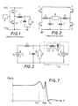
- switching devices which can be schematically described as a pair of switches controlled at a high switching frequency which switch the current to the load in an alternating way.
- the timing of the switching instants follows a modulation criterion according to the signal to be reproduced.
- the output signal consisting of the sum of the carrier signal and the modulating signal, is demodulated in a low-pass filter which extracts the low-frequency modulating signal from the high-frequency carrier.
- a diagram of an amplifier and of a corresponding low-pass filter of this type which are currently known is provided in Fig. 1.
- the numbers 1 and 3 indicate two electronic switches controlled by a PWM circuit indicated in a general way by 5.
- the chopped signal at the output is sent to a low-pass filter formed by a single L-C network comprising an inductance L and a capacitance C.
- the L-C network has a cut-off frequency of the order of 25 kHz to eliminate the high-frequency switching signal from the signal sent to the load Z, so that a signal containing only the frequencies in the audio range is supplied to the load (for example a loudspeaker) .
- the system may also be of the balanced type, in other words with a bridge configuration of the type illustrated in Fig. 2, where the load Z is disposed between two pairs of controlled switches 1, 3 and 1', 3'.
- the control signals of the two pairs of switches 1, 3 and 1', 3' are equal but in opposite phase.
- the symbols L, C and L', C' indicate the components of the low-pass output filters.
- the purpose of the present invention is to provide an output filter for a switching system of the type mentioned above which overcomes the disadvantages of conventional filters.
- the solution proposed by the invention consists in configuring the output filter on the basis of an L-C network, with attenuation and phase characteristics in the pass band that are acceptable in terms of quality, and adding to this a dipole or cancellation network which provides a very high attenuation at the switching frequency and a minimum effect in the pass band.
- the dipole generates a signal equal and opposite to the switching residue at the terminals of the load, in such a way that the sum of the two signals is canceled and no current at the switching frequency flows to the load.
- the resonant frequency of the L-C network is lower than the switching frequency, so that it presents an inductive behavior to the generator.
- the symbol Z indicates in a general way the load to be supplied and L and C again indicate, as in Fig. 1, the inductance and capacitance of the L-C network of the filter.
- the symbol V1 indicates schematically the signal source, which contains both the modulated signal and the switching signal.
- the number 11 indicates in a general way the cancellation dipole connected in parallel to the load Z. It comprises a generator V2 and an impedance X, consisting of an inductance Lx and a capacitance Cx in series. Additionally, in the diagram in Fig.
- the symbols I 1 , I 2 and I 3 indicate, respectively, the current flowing in the inductance L, the current flowing in the inductance Lx and the current in the load Z.
- the correct operation of the filter implies that the value of X is equal to the nominal value V 2 /I 2 at the switching frequency w c and at the highest possible value (tending towards infinity) in the pass band, in order that the cancellation dipole interferes to the least possible extent with the characteristics determined by the L-C network.
- Fig. 7 shows an example of the response of the filter: the horizontal axis shows the frequencies and the vertical axis shows the output voltage.
- the cancellation frequency is indicated by Fc.
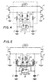
- the load is again indicated by Z and in parallel to it there is connected a serial RC circuit, consisting of the resistor Rp and the capacitor Cp, to prevent undamped resonances in the absence of the load Z.
- the load is connected as a bridge between two voltage generators, each consisting of a corresponding pair of driven switches, 1, 3 and 1', 3' respectively.
- the two pairs of switches 1, 3 and 1', 3' are driven by the same switching signal but in antiphase. This ensures an optimal symmetry in the two branches which can differ from each other only by the small tolerances between the driving devices and the power switches.
- Each of the two impedances consists of an inductance Lx and Lx' in series with a capacitance Cx and Cx' respectively.
- the system shown in Fig. 4 is balanced only in a theoretical way, whereas in the practical embodiment the tolerances on the individual components may include differences in the currents flowing in the two branches.
- the two inductances L and L' can be coupled by winding them on a common magnetic core.
- the value of the overall inductance must be equal to the sum of the two individual inductances L and L'.
- a number of turnings which is smaller (by a factor of 2 -1/2 ) than the total number of turnings to be used in the case of non-coupled inductances will therefore be used. This results in a reduction of the ohmic losses in the winding and a reduction in volume, in addition to an advantage in terms of current equalization.
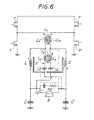
- the imperfect mirror image configuration of the real system may also be manifested in common-mode disturbances due to the switching residue.
- the common-mode cancellation is achieved by coupling the inductances Lx and Lx' by winding them on the same magnetic core.
- the same considerations are applicable in respect of the number of turnings, and consequently this coupling also permits a reduction of the number of turnings and therefore of the losses in the conductor and of the dimensions.
- the result is the circuit shown in Fig. 5, where identical or equivalent elements are indicated by the same reference numbers as those used in the diagram in Fig. 4.
- the symbol T indicates the winding core of the inductances L and L'
- Tx indicates the winding core of the inductances Lx, Lx'.
- any difference between the switching instants of the two generators 1, 3 and 1', 3' can be considered as a phase difference and therefore as a common-mode disturbance in the output signal.
- This disturbance is eliminated with a common-mode filter which may consist of two coupled inductances as shown in the diagram in Fig. 6, where the common-mode filter consists of two inductances Lm and Lm', wound on the common core Tm.
- the remaining components are indicated by the same reference numbers as those used in the diagram in Fig. 5.
Landscapes
- Engineering & Computer Science (AREA)
- Power Engineering (AREA)
- Amplifiers (AREA)
- Networks Using Active Elements (AREA)
- Filters And Equalizers (AREA)
Claims (13)
- Filter zur Unterdrückung eines Trägersignals in einem modulierten Signal, welches durch eine Schaltung erzeugt ist, die eine Last (Z) speist, mit einer Filterschaltung (L, C; L', C'), gekennzeichnet durch ein Löschnetzwerk (Lx, Cx, V2; Lx, Cx, Lx', Cx'), das vom Ausgangssignal einen Strom gleich dem Restträgersignal, welches durch die Filterschaltung (L, C, L', C') hindurchgeht, subtrahiert.
- Filter nach Anspruch 1,
dadurch gekennzeichnet , daß die Filterschaltung (L, C; L', C') ein L-C-Netzwerk aufweist. - Filter nach Anspruch 1,
dadurch gekennzeichnet , daß das Löschnetzwerk aufweist einen Spannungsgenerator (V2) in Gegenphase zum Spannungsgenerator (V1), der die Last (Z) speist und eine Impedanz mit einer in Reihe geschalteten Induktanz (Lx) und Kapazitanz (Cx). - Filter nach Anspruch 2 oder 3,
dadurch gekennzeichnet, daß die Induktanz (Lx) und die Kapazitanz (Cx) des Löschnetzwerkes und die Induktanz des L-C-Netzwerkes der Ausgangsfilterschaltung zueinander und zur Frequenz wc des Trägersignals korreliert sind durch die Gleichung: - Filter nach einem der vorstehenden Ansprüche,
gekennzeichnet durch eine abgeglichene Brückenstruktur. - Filter nach Anspruch 5,
dadurch gekennzeichnet , daß die zwei Verbindungspole der Last (Z) mit zwei Generatoren (1,3; 1', 3'). in Gegenphase verbunden sind, und daß jeder Verbindungspol der Last (Z) einer Filterschaltung (L, C; L', C') zugeordnet ist, wobei das Löschnetzwerk (Lx, Cx; Lx', Cx') zwei symmetrische Zweige aufweist, die jeweils die Mitte jeder Halbbrücke (1, 3; 1', 3') mit dem entgegengesetzten Verbindungspol der Last (Z) verbinden. - Filter nach Anspruch 6,
dadurch gekennzeichnet , daß jede der Filterschaltungen (L, C; L', C'), die mit den zwei Verbindungspolen der Last verbunden ist, eine Induktanz (L; L') in Reihe mit einer entsprechenden Kapazitanz (C; C') hat. - Filter nach Anspruch 7,
dadurch gekennzeichnet , daß die Induktanzen (L, L') der zwei Filterschaltungen zusammengekoppelt und auf einen gemeinsamen Kern (T) gewickelt sind. - Filter nach Anspruch 6, 7 oder 8,
dadurch gekennzeichnet , daß jeder Zweig des Löschnetzwerkes eine Induktanz (Lx, Lx') in Reihe zu einer entsprechenden Kapazitanz (Cx, Cx') aufweist. - Filter nach Anspruch 9,
dadurch gekennzeichnet , daß die Induktanzen (Lx, Lx') der zwei Zweige des Löschnetzwerkes zusammengekoppelt und auf einen gemeinsamen Kern (Tx) gewickelt sind. - Filter nach einem oder mehreren der Ansprüche 5 bis 10, dadurch gekennzeichnet , daß das Filter zusätzlich ein Gleichtaktfilter (Lm, Lm', Tm) aufweist.
- Filter nach Anspruch 11,
dadurch gekennzeichnet , daß das Gleichtaktfilter zwei Induktanzen (Lm, Lm') aufweist, die auf einen gemeinsamen Kern (Tm) gewickelt sind. - Filter nach einem oder mehreren der vorstehenden Ansprüche,
dadurch gekennzeichnet , daß das Filter in einen Tonfrequenzbandverstärker eingebaut ist.
Applications Claiming Priority (3)
| Application Number | Priority Date | Filing Date | Title |
|---|---|---|---|
| IT97FI000027A IT1291783B1 (it) | 1997-02-21 | 1997-02-21 | Un filtro di ricostruzione per l'eliminazione del residuo di commutazione in un sistema a commutazione o simile |
| ITFI970027 | 1997-02-21 | ||
| PCT/IT1998/000031 WO1998037628A1 (en) | 1997-02-21 | 1998-02-19 | A reconstruction filter for eliminating the switching residue in a switched system or similar |
Publications (2)
| Publication Number | Publication Date |
|---|---|
| EP0962049A1 EP0962049A1 (de) | 1999-12-08 |
| EP0962049B1 true EP0962049B1 (de) | 2001-10-31 |
Family
ID=11351945
Family Applications (1)
| Application Number | Title | Priority Date | Filing Date |
|---|---|---|---|
| EP98905617A Expired - Lifetime EP0962049B1 (de) | 1997-02-21 | 1998-02-19 | Rekonstruktionsfilter zur unterdrückung von schaltrestströmen in einem geschalteten system oder ähnlichem |
Country Status (5)
| Country | Link |
|---|---|
| US (1) | US6281767B1 (de) |
| EP (1) | EP0962049B1 (de) |
| DE (1) | DE69802264T2 (de) |
| IT (1) | IT1291783B1 (de) |
| WO (1) | WO1998037628A1 (de) |
Families Citing this family (11)
| Publication number | Priority date | Publication date | Assignee | Title |
|---|---|---|---|---|
| US6768375B2 (en) * | 1998-11-12 | 2004-07-27 | Jam Technologies, Llc | Multi-reference high accuracy switching amplifier expansion |
| CN1199349C (zh) * | 1998-11-12 | 2005-04-27 | 拉里·科恩 | 多基准高精度开关放大器 |
| WO2001091287A1 (en) * | 2000-05-25 | 2001-11-29 | Koninklijke Philips Electronics N.V. | Demodulation filter |
| US6744311B2 (en) * | 2001-04-23 | 2004-06-01 | Jam Technologies, Llc | Switching amplifier with voltage-multiplying output stage |
| KR100423399B1 (ko) * | 2001-11-05 | 2004-03-18 | 삼성전기주식회사 | 다연 노이즈저감 필터 |
| KR100542793B1 (ko) * | 2002-05-08 | 2006-01-20 | (주)펄서스 테크놀러지 | 디지털 오디오 증폭기의 복조장치 |
| US7932777B1 (en) * | 2003-03-24 | 2011-04-26 | Zipfel Jr George Gustave | Switching amplifier for driving reactive loads |
| CA2616220A1 (en) * | 2005-07-28 | 2007-02-08 | Rgb Systems, Inc. | Method and apparatus for implementing soft switching in a class d amplifier |
| US8310305B1 (en) * | 2011-04-14 | 2012-11-13 | Rockwell Collins, Inc. | Tapered-impedance distributed switching power amplifiers |
| DE102014200964A1 (de) * | 2014-01-21 | 2015-07-23 | Robert Bosch Gmbh | Verstärkeranordnung mit Tiefpassfiltereinrichtung |
| FR3055173B1 (fr) * | 2016-08-22 | 2019-08-16 | Devialet | Dispositif d'amplification comprenant un circuit de compensation |
Family Cites Families (6)
| Publication number | Priority date | Publication date | Assignee | Title |
|---|---|---|---|---|
| US4186437A (en) * | 1978-05-03 | 1980-01-29 | California Institute Of Technology | Push-pull switching power amplifier |
| JPS5582516A (en) * | 1978-12-19 | 1980-06-21 | Toshiba Corp | Amplitude modulator |
| US4628275A (en) * | 1985-07-29 | 1986-12-09 | Rockwell International Corporation | Efficient power amplifier for high capacitive devices |
| DE4007566C2 (de) * | 1990-03-09 | 1998-07-16 | Siemens Ag | Leistungsverstärker für die Speisung einer Induktivität mit geschalteten Transistoren |
| DE19512754A1 (de) * | 1995-04-05 | 1996-10-10 | Thomson Brandt Gmbh | Leistungsverstärker |
| US5657219A (en) * | 1995-08-29 | 1997-08-12 | Crown International, Inc. | Opposed current power converter |
-
1997
- 1997-02-21 IT IT97FI000027A patent/IT1291783B1/it active IP Right Grant
-
1998
- 1998-02-19 WO PCT/IT1998/000031 patent/WO1998037628A1/en not_active Ceased
- 1998-02-19 DE DE69802264T patent/DE69802264T2/de not_active Expired - Fee Related
- 1998-02-19 US US09/367,708 patent/US6281767B1/en not_active Expired - Fee Related
- 1998-02-19 EP EP98905617A patent/EP0962049B1/de not_active Expired - Lifetime
Also Published As
| Publication number | Publication date |
|---|---|
| ITFI970027A1 (it) | 1998-08-21 |
| ITFI970027A0 (it) | 1997-02-21 |
| EP0962049A1 (de) | 1999-12-08 |
| IT1291783B1 (it) | 1999-01-21 |
| DE69802264T2 (de) | 2002-08-22 |
| US6281767B1 (en) | 2001-08-28 |
| DE69802264D1 (de) | 2001-12-06 |
| WO1998037628A1 (en) | 1998-08-27 |
Similar Documents
| Publication | Publication Date | Title |
|---|---|---|
| EP0962049B1 (de) | Rekonstruktionsfilter zur unterdrückung von schaltrestströmen in einem geschalteten system oder ähnlichem | |
| US6856230B2 (en) | Harmonic filtering circuit with special transformer | |
| US7667988B2 (en) | Filter | |
| CA1169359A (en) | Step-up circuit for driving full-range-element electrostatic loudspeakers | |
| JPH02177605A (ja) | パルス幅変調増幅回路 | |
| EP4315545B1 (de) | Filter zur unterdrückung der elektromagnetischen interferenz | |
| CA2580104A1 (en) | Improved power converter with reduced common mode voltage | |
| EP0683966A4 (de) | Elektronisches vorschaltgerät mit zwei transistoren und zwei transformatoren. | |
| CN103582822A (zh) | 用于电流测量的设备 | |
| JP4445063B2 (ja) | Adslスプリッタに適用可能なフィルタ構成 | |
| US11114992B2 (en) | Motor drive with a filter including a three-phase differential mode reactor with common mode damping | |
| US7378754B2 (en) | Three-phase harmonic reduction filter for bidirectional power converters | |
| JPH08126201A (ja) | キャリア成分抑制方法 | |
| US11114932B1 (en) | Method and apparatus for reduction of ripple current | |
| US4238644A (en) | Supply circuit for a subscriber's line circuit | |
| JP3539405B2 (ja) | 搬送波フィルタ | |
| EP0995266A1 (de) | Netzfilteranordnung | |
| FI122088B (fi) | Nousevan taajuusvasteen kompensointi virtaohjatussa passiivikaiuttimessa | |
| US9973001B2 (en) | Zero sequence, fifth harmonic filter for five-phase power distribution system | |
| RU2335082C1 (ru) | Электромагнитный компенсатор гармоник | |
| CN110518886A (zh) | 一种逆f功率放大器的电感耦合匹配电路 | |
| JP3159459B2 (ja) | 電気機器における感電を防止するラインフィルター | |
| KR101675166B1 (ko) | 노이즈에 대한 필터 기능이 포함된 트랜스포머 | |
| JPH03296313A (ja) | 電力線搬送通信用の単相三線式ブロッキングフィルタ | |
| JP3203473B2 (ja) | 節電装置 |
Legal Events
| Date | Code | Title | Description |
|---|---|---|---|
| PUAI | Public reference made under article 153(3) epc to a published international application that has entered the european phase |
Free format text: ORIGINAL CODE: 0009012 |
|
| 17P | Request for examination filed |
Effective date: 19990730 |
|
| AK | Designated contracting states |
Kind code of ref document: A1 Designated state(s): DE ES FR GB NL |
|
| GRAG | Despatch of communication of intention to grant |
Free format text: ORIGINAL CODE: EPIDOS AGRA |
|
| 17Q | First examination report despatched |
Effective date: 20001206 |
|
| GRAG | Despatch of communication of intention to grant |
Free format text: ORIGINAL CODE: EPIDOS AGRA |
|
| GRAH | Despatch of communication of intention to grant a patent |
Free format text: ORIGINAL CODE: EPIDOS IGRA |
|
| GRAH | Despatch of communication of intention to grant a patent |
Free format text: ORIGINAL CODE: EPIDOS IGRA |
|
| GRAA | (expected) grant |
Free format text: ORIGINAL CODE: 0009210 |
|
| AK | Designated contracting states |
Kind code of ref document: B1 Designated state(s): DE ES FR GB NL |
|
| PG25 | Lapsed in a contracting state [announced via postgrant information from national office to epo] |
Ref country code: NL Free format text: LAPSE BECAUSE OF FAILURE TO SUBMIT A TRANSLATION OF THE DESCRIPTION OR TO PAY THE FEE WITHIN THE PRESCRIBED TIME-LIMIT Effective date: 20011031 Ref country code: FR Free format text: LAPSE BECAUSE OF FAILURE TO SUBMIT A TRANSLATION OF THE DESCRIPTION OR TO PAY THE FEE WITHIN THE PRESCRIBED TIME-LIMIT Effective date: 20011031 |
|
| REF | Corresponds to: |
Ref document number: 69802264 Country of ref document: DE Date of ref document: 20011206 |
|
| REG | Reference to a national code |
Ref country code: GB Ref legal event code: IF02 |
|
| NLV1 | Nl: lapsed or annulled due to failure to fulfill the requirements of art. 29p and 29m of the patents act | ||
| PG25 | Lapsed in a contracting state [announced via postgrant information from national office to epo] |
Ref country code: ES Free format text: LAPSE BECAUSE OF FAILURE TO SUBMIT A TRANSLATION OF THE DESCRIPTION OR TO PAY THE FEE WITHIN THE PRESCRIBED TIME-LIMIT Effective date: 20020430 |
|
| PLBE | No opposition filed within time limit |
Free format text: ORIGINAL CODE: 0009261 |
|
| STAA | Information on the status of an ep patent application or granted ep patent |
Free format text: STATUS: NO OPPOSITION FILED WITHIN TIME LIMIT |
|
| 26N | No opposition filed | ||
| PGFP | Annual fee paid to national office [announced via postgrant information from national office to epo] |
Ref country code: GB Payment date: 20040218 Year of fee payment: 7 |
|
| PGFP | Annual fee paid to national office [announced via postgrant information from national office to epo] |
Ref country code: DE Payment date: 20040421 Year of fee payment: 7 |
|
| PG25 | Lapsed in a contracting state [announced via postgrant information from national office to epo] |
Ref country code: GB Free format text: LAPSE BECAUSE OF NON-PAYMENT OF DUE FEES Effective date: 20050219 |
|
| PG25 | Lapsed in a contracting state [announced via postgrant information from national office to epo] |
Ref country code: DE Free format text: LAPSE BECAUSE OF NON-PAYMENT OF DUE FEES Effective date: 20050901 |
|
| GBPC | Gb: european patent ceased through non-payment of renewal fee |
Effective date: 20050219 |