EP0961450B1 - Detection of frequency errors in multicarrier receivers - Google Patents
Detection of frequency errors in multicarrier receivers Download PDFInfo
- Publication number
- EP0961450B1 EP0961450B1 EP99304137A EP99304137A EP0961450B1 EP 0961450 B1 EP0961450 B1 EP 0961450B1 EP 99304137 A EP99304137 A EP 99304137A EP 99304137 A EP99304137 A EP 99304137A EP 0961450 B1 EP0961450 B1 EP 0961450B1
- Authority
- EP
- European Patent Office
- Prior art keywords
- cycle prefix
- components
- signal
- circuit
- output
- Prior art date
- Legal status (The legal status is an assumption and is not a legal conclusion. Google has not performed a legal analysis and makes no representation as to the accuracy of the status listed.)
- Expired - Lifetime
Links
Images


Classifications
-
- H—ELECTRICITY
- H04—ELECTRIC COMMUNICATION TECHNIQUE
- H04B—TRANSMISSION
- H04B7/00—Radio transmission systems, i.e. using radiation field
- H04B7/14—Relay systems
- H04B7/15—Active relay systems
- H04B7/204—Multiple access
-
- H—ELECTRICITY
- H04—ELECTRIC COMMUNICATION TECHNIQUE
- H04L—TRANSMISSION OF DIGITAL INFORMATION, e.g. TELEGRAPHIC COMMUNICATION
- H04L27/00—Modulated-carrier systems
- H04L27/26—Systems using multi-frequency codes
- H04L27/2601—Multicarrier modulation systems
- H04L27/2647—Arrangements specific to the receiver only
- H04L27/2655—Synchronisation arrangements
- H04L27/2668—Details of algorithms
- H04L27/2673—Details of algorithms characterised by synchronisation parameters
- H04L27/2676—Blind, i.e. without using known symbols
- H04L27/2678—Blind, i.e. without using known symbols using cyclostationarities, e.g. cyclic prefix or postfix
-
- H—ELECTRICITY
- H04—ELECTRIC COMMUNICATION TECHNIQUE
- H04L—TRANSMISSION OF DIGITAL INFORMATION, e.g. TELEGRAPHIC COMMUNICATION
- H04L27/00—Modulated-carrier systems
- H04L27/26—Systems using multi-frequency codes
- H04L27/2601—Multicarrier modulation systems
- H04L27/2647—Arrangements specific to the receiver only
- H04L27/2655—Synchronisation arrangements
- H04L27/2657—Carrier synchronisation
Definitions
- the present invention relates to a receiving method and a receiving apparatus for receiving a signal subjected to an orthogonal frequency division multiplexing (to be referred to as an OFDM hereinafter) modulation and, more particularly, to a technique for detecting a frequency error of a received signal.
- an orthogonal frequency division multiplexing to be referred to as an OFDM hereinafter
- the OFDM modulation system is a system for transmitting transmission data as a multi-carrier which is dispersed into a plurality of sub-carriers. This modulation system can efficiently transmit a large-capacity data in a wireless mode.
- a wireless transmission state of a signal subjected to the OFDM modulation there may be such a case that one unit of OFDM modulation signal is continuously transmitted in a predetermined frequency band.
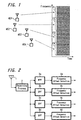
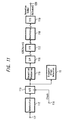
- OFDM modulation signals transmitted in a wireless mode from a plurality of mobile stations MS1, MS2, MS3, and MS4 are subjected to a receiving process by a base station.
- the OFDM modulation signals from the respective mobile stations MS1 to MA4 are transmitted as multi-carrier signals respectively using different bands F1 to F4, and all the bands F1 to F4 are subjected to a receiving process by the base station.
- a system in which multi-connection between the base station and a plurality of surrounding mobile stations is made by using OFDM modulation waves as described above has been proposed.
- FIG. 2 is a diagram showing an example of a circuit arrangement for detecting a frequency offset in a conventional base station. This example is a case wherein the frequency offsets of signals from the four mobile stations MS1 to MS4 shown in FIG. 1 are detected.
- a receiving processor 2 connected to an antenna 1 performs the signals of the transmission bands at once, and then the received signals are supplied to four band-pass filters 3a, 3b, 3c, and 3d having different passing bands, respectively. In this case, the passing bands of the band-pass filters 3a to 3d are set for the transmission bands F1 to F4 shown in FIG. 1, respectively.
- Outputs from the band-pass filters 3a to 3d are supplied to different frequency offset detection circuits 4a, 4b, 4c, and 4d, respectively.
- the frequency offsets of transmission signals from the four mobile stations MS1 to MS4 are independently subjected to a detection process by the frequency offset detection circuits 4a to 4d, respectively.
- the following correction process is performed. That is, the reception frequencies of signals transmitted from the mobile stations are corrected, or data for correcting a frequency offset is transmitted to a corresponding mobile station.
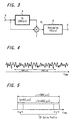
- a detection process using a cycle prefix component included in an OFDM modulation signal is known.
- An example of a frequency offset detection arrangement using the cycle prefix component is shown in Fig. 3.
- a similar arrangement for detecting the frequency offset to that shown in Fig. 3 is disclosed in Sandell et al., "Timing And Frequency Synchronisation In OFDM Systems Using The Cycle Prefix", International Symposium On Synchronisation, December 1995, pp 16-19.
- a signal from a terminal 5 at which an output from each of the band-pass filters 3a to 3d can be obtained is supplied to a multiplier 7 through a delay circuit 6 for delaying the signal for a predetermined period, and a signal obtained at the terminal 5 is directly supplied to the terminal 5. Both the signals are subjected to a multiplying process.
- an amount of delay of the delay circuit 6 is set to be an inherent amount of delay included in the cycle prefix component. The relationship between the cycle prefix component and the amount of delay will be described later.
- the signal delayed by the delay circuit 6 is a complex signal. A multiplying process of a complex conjugate is performed in the multiplier 7.
- An output from the multiplier 7 is supplied to an averaging circuit 8 to calculate an average in a predetermined period, and the average value is supplied to an output terminal 9 as a value which is in proportion to a frequency offset value.
- the period in which averaging is performed by the averaging circuit 8 is set to be a period corresponding to one length (time) of a cycle prefix component, for example. With such a process, a value which is in proportion to the frequency offset value is obtained at the output terminal 9.
- Equation (2) equation an OFDM modulation signal before windowing for transmission
- Equation (3) The OFDM modulation signal represented by Equation (2) and obtained before windowing is performed can also expressed as represented by the following Equation (3).
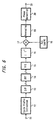
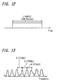
- an OFDM signal obtained before windowing is performed has, for example, as shown in FIG. 4, a signal waveform having a periodicity of 240 [ ⁇ s].
- a transmission window When the OFDM modulation signal is to be transmitted, the process for multiplying windowing data (time waveform) called a transmission window.
- a signal obtained by multiplying the windowing data is represented by the following equation.
- w(t) denotes windowing data (window).
- FIG. 5 is a diagram showing an example of windowing data.
- a window is represented by an rectangular wave, and the window is set to be a window in a period L (280 [ ⁇ s]) obtained by adding a period T g (40 [ ⁇ s]) to the above-mentioned period T c (240 ⁇ s]).
- an OFDM wave in the period T g at the start portion of one unit of window and an OFDM wave in the period T g , at the end portion, having a time width equal to that of the period T g at the start portion have completely an equal waveform.
- This modulation wave is called a cycle prefix.
- This cycle prefix corresponds to a cycle prefix CP shown in FIG. 5.
- the OFDM wave multiplied by the windowing data is represented by the following equation when a frequency offset of v [Hz] is put on the OFDM wave.
- signals d(t) having equal waveforms are repeated such that the signals are separated from each other by 240 [ ⁇ s] and rotated by a phase a [rotation].
- a frequency error was detected by using the cycle prefix component. That is, when the frequency offset detection circuit described above and shown in FIG. 3 detects the frequency offset of the OFDM wave multiplied by windowing data shown in FIG. 5, 240 [ ⁇ s] is set as an amount of delay of the delay circuit 6, and 40 [ ⁇ s] is set as a period in which averaging is performed by the averaging circuit 8.
- Equation 8 represents a state wherein a frequency error is detected by the circuit in FIG. 3, and a frequency error can be detected by calculating the phase of the value of a complex number q.
- the frequency offset detection circuits are required for respective receiving system of signals from the mobile stations, and a base station must have a plurality of the frequency offset detection circuits each shown in FIG. 14.
- the base station is disadvantageously complex in arrangement.
- a receiving method of determining a frequency error of a received OFDM modulation signal characterised by comprising the steps of:
- the frequency error of the received OFDM modulation signal can be easily determined on the basis of the detected phase shift.
- said step of detecting the phase shift comprises:
- said step of Fourier transforming the extracted cycle prefix components comprises: narrowing a time interval between the two signal components constituting the extracted cycle prefix components; and performing a Fourier transformation of the thus processed cycle prefix components. Therefore, the number of transform points in the Fourier transformation can be reduced in accordance with the narrowed time range, and an amount of transform process in the Fourier transformation can be decreased.
- said step of Fourier transforming the extracted cycle prefix components comprises: narrowing the time interval between the two signal components constituting the cycle prefix components; and performing the Fourier transformation in a time range which is four times the shortened repetitive time of the two signal components; and a cycle used when detecting the phase shift of the envelope of said square values is set to be four. Therefore, a process for phase detection can be performed by only selection of a real number or an imaginary number and sign inversion, and phase detection can be performed by a simple process.
- a receiving apparatus comprising means for determining a frequency error of a received OFDM modulation signal, characterised by said means comprising:
- the frequency error of the received OFDM modulation signal can be determined by a simple arrangement for detecting a phase.
- said detection means comprises: an orthogonal detecting means for performing orthogonal detection of the output of the absolute value square means at the sub-carrier interval of the OFDM symbol; an average value calculation means for calculating an average value of the orthogonally detected signal output by the orthogonal detection means; and a phase detection means for detecting the phase of the complex number output from the average value calculation means. Therefore, a phase value which is in proportion to the frequency error can be detected by a simple arrangement constituted by the Fourier transformation means, the average value calculation means, and the phase detection means.
- said detection means comprises: a cycle prefix component shift means for narrowing a time interval between the two signal components constituting the extracted cycle prefix components output by the cycle prefix component extraction means, the Fourier transformation means being arranged Fourier transform the output from the cycle prefix component shift means. Therefore, the number of transform points in the Fourier transformation means can be decreased in accordance with the shifted time interval, and a simple arrangement having a small number of transform points can be used as the Fourier transformation means.
- the Fourier transformation means is arranged to perform a Fourier transform in a time range which is four times the shortened repetitive time of the two signal components output by the cycle prefix component shift means, and a cycle used in the detection performed by the detection means is set to be four. Therefore, a process arrangement for phase detection can be realized by only selection of a real number or an imaginary number and sign inversion, and phase detection can be performed by a simple arrangement.
- the hereinafter described embodiment of the present invention can make it possible to detect a frequency offset in reception state of an OFDM modulation signal with a simple arrangement.
- the present invention is applied to a wireless communication device for performing a receiving process for an OFDM modulation signal.
- a transmission arrangement for the OFDM modulation signal will be described below with reference to FIG. 9.
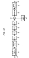
- a signal is modulated into an OFDM signal in which the number of sub-carriers is 96, and a sub-carrier interval is set to be 4.1666 [kHz].
- Data of transmission symbols (in this case, one unit is constituted by 96 symbols) obtained from an input terminal 111 is supplied to a serial/parallel conversion circuit 102 to be converted into 96-point parallel data.
- the parallel data is supplied to a zero insertion circuit 103 to be added with 32-point 0 data, thereby obtaining 128-point parallel data.
- the 128-point parallel data are supplied to an inverse Fourier transformation circuit (IFFT circuit) 104 having 128 points.
- IFFT circuit inverse Fourier transformation circuit
- the resultant data is subjected to an orthogonal transform process for transforming a time axis into a frequency axis by using inverse fast Fourier transformation.
- the process of adding 32-point 0 data in the zero insertion circuit 103 is performed for the following reason. That is, the number of points is set to be a power of 2 (in this case, 128) to make the arrangement of an inverse Fourier transformation process circuit simple.
- a conversion output from the inverse Fourier transformation circuit 104 is output to a parallel/serial conversion circuit 105 to be converted into serial data, and the serial data is supplied to a transmission windowing data multiplying circuit 106 to be multiplied by transmission windowing data.
- a predetermined period T c in this case 240 [ps]
- a 21-point period T g in this case, 40 [ps]
- the cycle prefix CP of the 21-point period T g at the start portion and the cycle prefix CP of the 21-point period T g at the end portion have completely the same waveform.
- the windowing data is shown as a rectangular wave. However, in fact, the windowing data is not a rectangular wave in many cases (the same as in the case of transmission windowing data to be described later).
- Transmission data multiplied by windowing data in the transmission windowing data multiplying circuit 106 is supplied to a digital/analog converter 107 to be converted into an analog signal at a sampling cycle based on a predetermined-frequency clock (clock of 533.33 [kHz] which is a value obtained by multiplying a sub-carrier interval of 4.1666 [kHz] by the number of points, i.e., 128) obtained from a terminal 108.
- the converted signal is supplied to a modulation circuit 109 to be subjected to a transmission modulation process.
- the modulated signal is supplied from a terminal 110 to a transmission process circuit (not shown), and the frequency of the signal is converted into a predetermined transmission frequency.
- the frequency-converted signal is transmitted in a wireless mode.
- FIG. 11 An arrangement for receiving the OFDM modulation signal transmitted in a wireless mode as described above is shown in FIG. 11.
- a signal having a predetermined frequency band is received, and the signal which is frequency-converted into an intermediate-frequency signal or the like is obtained from an input terminal 111.
- the signal obtained at the input terminal 111 is supplied to a demodulation circuit 112 to be subjected to a reception modulation process.
- the demodulated signal is supplied to a analog/digital converter 113 to be converted into digital data in a sampling cycle based on a predetermined-frequency clock (in this case, 533.33 [kHz]: this clock has a frequency equal to that of a clock at a transmission process) obtained from a terminal 114.
- a predetermined-frequency clock in this case, 533.33 [kHz]: this clock has a frequency equal to that of a clock at a transmission process
- the converted data is supplied to a reception windowing data multiplying circuit 115 to be multiplied by reception windowing data.
- a reception windowing data for example, as shown in FIG. 10, a time L (in this case, 240 [ ⁇ s]) for selecting 128-point data is set.
- the received data multiplied by the reception windowing data is supplied to a serial/parallel conversion circuit 116 to be converted into parallel data at every predetermined unit.
- the converted output is supplied to a Fourier transformation circuit (FFT circuit) 117, and an orthogonal transform process for transforming a frequency axis into a time axis is performed by a calculation process using fast Fourier transformation.
- FFT circuit Fourier transformation circuit
- the parallel data subjected to orthogonal transformation is supplied to a demultiplexer 118, and predetermined-point data are selected.
- the selected data is supplied to a parallel/serial conversion circuit 119 to be converted into serial data, and the serial data is supplied to an output terminal 120.
- the received data converted by the analog/digital converter 113 is supplied to a frequency offset detection circuit 10.
- FIG. 6 shows the arrangement of the frequency offset detection circuit 10 of this embodiment.
- the received data converted by the analog/digital converter 113 is supplied to a cycle prefix extraction circuit 12 through a terminal 11.
- the process of extracting only a cycle prefix component in the received data and setting all the remaining data to be 0 data is performed. More specifically, in this embodiment, the windowing data shown in FIG. 10 is multiplied at a transmission time, and data in which a cycle prefix CP is generated is transmitted.
- the cycle prefix extraction circuit 12 as shown in, for example, FIG. 7, only 21 points corresponding to the periods T g (in this case, 40 [ ⁇ s]) of cycle prefix components at the start portion and the end portion of one window each are extracted, and all 107-point data therebetween are set to be 0 data.
- An output from the cycle prefix extraction circuit 12 is supplied to a serial/parallel conversion circuit 13 to be converted into parallel data, the parallel data is supplied to a Fourier transformation circuit (FFT circuit) 14, and an orthogonal transform process for transforming a frequency axis into a time axis is performed by a calculation process using fast Fourier transformation.
- the number of points converted by the serial/parallel conversion circuit 13 and the number of points subjected to the transform process by the FFT circuit 14 are determined to be the number of points falling in the range which is sufficiently larger than the number of points corresponding to a repetitive distance of the cycle prefix component.
- the number of points subjected to the transform process by the FFT circuit 14 is represented by N
- the number of points corresponding to the repetitive distance of the cycle prefix component is represented by M.
- the repetitive distance M 128 points
- the parallel data subjected to orthogonal transformation by the FFT circuit 14 is supplied to a parallel/serial conversion circuit 15 to be converted into serial data, and the serial data is supplied to an absolute value square circuit 16.
- a value is obtained by squaring the absolute value of the serial data.
- the value squared by the absolute value square circuit 16 is supplied to a multiplier 17 to be multiplied by a multiplying coefficient Rot (kM/N) output from a multiplying coefficient generation circuit 18.
- the value multiplied by the coefficient in the multiplier 17 is supplied to an averaging circuit 19 to be averaged in the period T g (in this case, 40 [ ⁇ s]) of one cycle prefix component.
- the averaged value (complex number) is supplied to a phase detection circuit 20.
- phase detection circuit 20 the phase value of the average value is detected, and the detected data is output from a terminal 21.
- a phase detection value obtained at the terminal 21 becomes a value which is in proportion to an amount of frequency offset of the received OFDM modulation signal. The amount of frequency offset can be judged on the basis of the phase detection value.
- the component of a cycle prefix CP is extracted from this OFDM modulation signal by the cycle prefix extraction circuit 12, and all the remaining data are set to be 0 data.
- the data extracted by the cycle prefix extraction circuit 12 is represented by the following equation. In this equation, as shown in FIG. 7, a cycle prefix CP at the start portion is represented by d(t), and a cycle prefix CP at the end portion is represented by d(t - Tc)rot(a).
- Equation (10) is subjected to Fourier transformation by the FFT circuit 14 to obtain Equation (11).
- Equation (12) since it is supposed that
- Equation (13) A signal obtained by Equation (13) is averaged on a frequency axis by the averaging circuit 19.
- E[] the average value of q is represented by the following equation.
- a frequency offset can be used as a coefficient. Therefore, with a simple arrangement in which squaring of the absolute value of a value subjected to Fourier transformation and a phase detection process are performed, a precise frequency offset can be detected.
- the number of points subjected to a transformation process by the FFT circuit 14 is represented by N
- the number of points corresponding to the repetitive distance of the cycle prefix component is represented by M.
- the number of transform process points N of Fourier transformation is set to be four times the repetitive distance M of the cycle prefix component. For this reason, a simple arrangement which does not require the multiplier 17 and the multiplying coefficient generation circuit 18 shown in FIG. 6 can also be used.
- a multiplying coefficient Rot(kM/N) generated by the multiplying coefficient generation circuit 18 is Rot(k/4).
- An arrangement in which multiplying is not performed can be used.
- An example of a circuit which can be replaced with the multiplier 17 is shown in FIG. 8.
- the sign selection circuits 33a, 33b, 33c, and 33d perform processes of selecting different states (real-number value or imaginary-number value and positive or negative), respectively. For example, the sign selection circuit 33a sets a real-number value and a positive sign, the sign selection circuit 33b sets an imaginary-number value and a positive sign, the sign selection circuit 33c sets a real-number value and a negative sign, and the sign selection circuit 33d sets an imaginary-number value and a negative value.
- Outputs from the respective sign selection circuits 33a, 33b, 33c, and 33d are supplied to a parallel/serial conversion circuit 34 to be returned to serial data, and the serial data is supplied from a terminal 35 to the averaging circuit 19 (see FIG. 6).
- the present invention can be realized by only selection of the real part or imaginary part of a signal and a sign inversion process in place of a multiplying process.
- the present invention is applied to a receiving apparatus which performs a receiving process for an OFDM modulation signal.
- the entire arrangement of a receiving apparatus according to this embodiment is the same as the arrangement shown in FIG. 11 and described in connection with the first embodiment described above.
- the number of sub-carriers (96) of a received OFDM modulation signal and a sub-carrier interval (4.1666 [kHz]) are set to be same as those in the embodiment described above.
- FIG. 14 shows the arrangement of a frequency offset detection circuit according to this embodiment. This arrangement will be described below.
- Received data converted by the analog/digital converter 113 shown in FIG. 11 is supplied to a cycle prefix extraction circuit 42 through a terminal 41.
- the cycle prefix extraction circuit 42 the process for extracting only a cycle prefix component in the received data and setting all the data of the remaining portion to be 0 data is performed. This process is the same process as described in the cycle prefix extraction circuit 12 in the first embodiment.
- Data constituted by only a cycle prefix CP at the start portion and a cycle prefix CP at the end portion shown in FIG. 15A is obtained.
- a repetitive interval of the cycle prefixes CP has 128 points (240 [ ⁇ s] as time).
- a signal extracted by the cycle prefix extraction circuit 42 is supplied to a waveform slide circuit 43, and the position of the cycle prefix at the start portion is slid to a position near the cycle prefix CP at the end portion.
- the repetitive interval between two cycle prefixes CP is set to be 32 points (60 [ ⁇ s] as time), and the number of points from the front end portion of the cycle prefix on the start side to the rear end portion of the cycle prefix on the end side is set to be 53 points.
- An output from the waveform slide circuit 43 is supplied to a serial/parallel conversion circuit 44 to be converted into parallel data, the parallel data is supplied to a Fourier transformation circuit (FFT circuit) 45, and an orthogonal transform process for transforming a frequency axis into a time axis is performed by a calculation process using fast Fourier transformation.
- the number of points converted by the serial/parallel conversion circuit 44 and the number of points subjected to the transform process by the FFT circuit 45 are determined to be the number of points falling in the range which is sufficiently larger than the number of points corresponding to a repetitive distance of the cycle prefix component.
- the repetitive distance M is set to be 32 points
- the parallel data orthogonally transformed by the FFT circuit 45 is supplied to a parallel/serial conversion circuit 46 to be converted into serial data, and the serial data is supplied to an absolute value square circuit 47.
- a value is obtained by squaring the absolute value of the serial data.
- the value squared by the absolute value square circuit 47 is supplied to a multiplier 48 to be multiplied by a multiplying coefficient Rot (kM/N) (Rot(k/4) when N is four times M as described above) output from a multiplying coefficient generation circuit 49.
- the value multiplied by the coefficient in the multiplier 48 is supplied to an averaging circuit 50 to be averaged in a period T g (in this case, 40 [ ⁇ s]) of one cycle prefix component.
- the averaged value (complex number) is supplied to a phase detection circuit 51.
- the phase value of the average value is detected, and the detected data is output from a terminal 52.
- a phase detection value obtained at the terminal 52 becomes a value which is in proportion to an amount of frequency offset of the received OFDM modulation signal. The amount of frequency offset can be determined on the basis of the phase detection value.
- a frequency offset can be detected by the arrangement of this embodiment is the same principle as described in Equation (9) to Equation (15) in the first embodiment described above, and a precise frequency offset can be preferably detected as in the first embodiment.
- the repetitive interval of cycle prefix components is shortened, the number of transform points in the Fourier transformation circuit 45 can be considerably reduced.
- the arrangement of the Fourier transformation circuit, and the serial/parallel conversion circuit and the parallel/serial conversion circuit arranged before and after the Fourier transformation circuit can be considerably simplified. A processing amount required for a calculation process can also be considerably reduced.
- the present invention is applied to a receiving apparatus for performing a receiving process for an OFDM modulation signal.
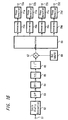
- a receiving apparatus is an example of a base station which simultaneously performs receiving processes of OFDM modulation signals from a plurality of mobile stations which are divided in bands and multi-connected (for example, a base station in a state shown in FIG. 1 as a prior art).
- the receiving apparatus has an arrangement which simultaneously receives signals from four mobile stations.
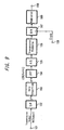
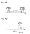
- FIG. 16 shows the arrangement of a frequency offset detection circuit according to this embodiment. This arrangement will be described below.
- Received data converted into digital data by an analog/digital converter (circuit corresponding to the analog/digital converter 113 in FIG. 11: Note that the circuit must be capable of simultaneously processing signals from a plurality of stations) of a circuit of a receiving system is supplied to a cycle prefix extraction circuit 62 through a terminal 61.
- the cycle prefix extraction circuit 62 the process of extracting only a cycle prefix component in the received data and setting all the data of the remaining portion to be 0 data is performed. This process is the same process as described in the cycle prefix extraction circuit 12 in the first embodiment.
- a waveform slid circuit may be provided to shorten a repetitive intervals of cycle prefixes CP.
- An output from the cycle prefix extraction circuit 62 is supplied to a serial/parallel conversion circuit 63 to be converted into parallel data, the parallel data is supplied to a Fourier transformation circuit (FFT circuit) 64, and an orthogonal transform process for transforming a frequency axis into a time axis is performed by a calculation process using fast Fourier transformation.
- the number of points converted by the serial/parallel conversion circuit 63 and the number of points subjected to the transform process by the FFT circuit 64 are determined to be the number of points falling in the range which is sufficiently larger than the number of points corresponding to a repetitive distance of the cycle prefix component output from the cycle prefix extraction circuit 62.
- the parallel data orthogonally transformed by the FFT circuit 64 is supplied to a parallel/serial conversion circuit 65 to be converted into serial data, and the serial data is supplied to an absolute value square circuit 66.
- a value is obtained by squaring the absolute value of the serial data.
- the value squared by the absolute value square circuit 66 is supplied to a multiplier 67 to be multiplied by a multiplying coefficient Rot (kM/N) output from a multiplying coefficient generation circuit 68.
- the signal multiplied by the coefficient in the multiplier 67 is supplied to a demultiplexer 69 to be divided into four signals in frequency bands (at every predetermined number of points) of an original signal.
- the respective divided signals are supplied to different averaging circuits 70a, 70b, 70c, and 70d, and averaging of a period T g (in this case, 40 [ ⁇ s]) of one cycle prefix component is performed in each circuit.
- the averaged values (complex numbers) are supplied to different phase detection circuits 71a to 71d, respectively.
- the phase detection circuits 71a to 71d detect phase values of the average values, and the detected data are output from output terminals 72a to 72d of the phase detection circuits 71a to 71d, respectively.
- Phase detection values obtained from the output terminals 72a to 72d become values which are in proportion to amounts of frequency offsets of the received OFDM modulation signals from the stations.
- the amounts of frequency offset of the signals transmitted from the respective mobile stations can be independently determined
- a frequency offset can be detected by the arrangement of this embodiment is the same principle as described in Equation (9) to Equation (15) in the first embodiment described above, and a precise frequency offset can be preferably detected as in the first embodiment.
- signals from a plurality of mobile stations are simultaneously processed in the arrangement used until coefficient multiplying is performed, these signals need not be processed by respectively arranging circuits for signals from the respective mobile stations.
- frequency offsets of the OFDM modulation signals simultaneously transmitted from a plurality of stations can be detected.
- the remaining portion can also be used in the arrangement of a Fourier transformation circuit.
- the number of transform points N subjected to Fourier transformation is set to be four times the number of points M corresponding to the repetitive distance of the cycle prefix component, in place of an arrangement for performing a coefficient multiplier, as shown in FIG. 8 described in the first embodiment, an arrangement for performing selection of a real number or an imaginary number and sign inversion can also be used.
- this arrangement shown in FIG. 8 is applied, the arrangement of the frequency offset detection circuit can be simplified further.
- the process of dividing signals from the respective stations is performed after the signals are multiplied by a coefficient.
- the circuit arrangement can be advantageously simplified by simultaneously processing signals from a plurality of stations.
Landscapes
- Engineering & Computer Science (AREA)
- Computer Networks & Wireless Communication (AREA)
- Signal Processing (AREA)
- Digital Transmission Methods That Use Modulated Carrier Waves (AREA)
- Mobile Radio Communication Systems (AREA)
- Synchronisation In Digital Transmission Systems (AREA)
- Monitoring And Testing Of Transmission In General (AREA)
Applications Claiming Priority (2)
| Application Number | Priority Date | Filing Date | Title |
|---|---|---|---|
| JP15033098 | 1998-05-29 | ||
| JP15033098A JP3915247B2 (ja) | 1998-05-29 | 1998-05-29 | 受信方法及び受信装置 |
Publications (3)
| Publication Number | Publication Date |
|---|---|
| EP0961450A2 EP0961450A2 (en) | 1999-12-01 |
| EP0961450A3 EP0961450A3 (en) | 2003-05-14 |
| EP0961450B1 true EP0961450B1 (en) | 2005-03-16 |
Family
ID=15494664
Family Applications (1)
| Application Number | Title | Priority Date | Filing Date |
|---|---|---|---|
| EP99304137A Expired - Lifetime EP0961450B1 (en) | 1998-05-29 | 1999-05-27 | Detection of frequency errors in multicarrier receivers |
Country Status (5)
| Country | Link |
|---|---|
| US (1) | US6381263B1 (enExample) |
| EP (1) | EP0961450B1 (enExample) |
| JP (1) | JP3915247B2 (enExample) |
| KR (1) | KR100567851B1 (enExample) |
| DE (1) | DE69924181T2 (enExample) |
Families Citing this family (15)
| Publication number | Priority date | Publication date | Assignee | Title |
|---|---|---|---|---|
| US6552995B1 (en) * | 1998-02-19 | 2003-04-22 | Advantest Corporation | Spectrum diffusion signal analyzer and method of analyzing diffusion signal |
| JP4378837B2 (ja) * | 2000-04-07 | 2009-12-09 | ソニー株式会社 | 受信装置 |
| EP1187387A1 (en) * | 2000-09-08 | 2002-03-13 | Alcatel | Multicarrier GSM receiver |
| KR100376804B1 (ko) * | 2000-09-29 | 2003-03-19 | 삼성전자주식회사 | 직교 주파수 분할 다중 방식 시스템의 주파수 옵셋 보상장치 및 방법 |
| KR100376803B1 (ko) * | 2000-09-29 | 2003-03-19 | 삼성전자주식회사 | 직교 주파수 분할 다중 방식 시스템의 주파수 옵셋 보상장치 및 방법 |
| US6950389B2 (en) * | 2001-02-16 | 2005-09-27 | Agere Systems Inc. | Peak-to-average power reduction in an orthogonal frequency division multiplexing system |
| KR100438570B1 (ko) * | 2001-08-23 | 2004-07-02 | 엘지전자 주식회사 | 무선 랜 수신기의 주파수 오차 검출 방법 |
| KR100640581B1 (ko) * | 2004-07-02 | 2006-10-31 | 삼성전자주식회사 | 상향 링크 통신시 엑세스 사용자의 주파수 옵셋을제어하는 직교 주파수 분할 다중 접속 시스템 및 주파수옵셋 제어 방법 |
| US7298772B1 (en) | 2004-09-03 | 2007-11-20 | Redpine Signals, Inc. | Packet detection, symbol timing, and coarse frequency estimation in an OFDM communications system |
| US20090279420A1 (en) * | 2005-01-11 | 2009-11-12 | Nec Corporation | Base station apparatus, radio transmission system, radio base station program, and timing estimation method |
| US20060224651A1 (en) * | 2005-03-31 | 2006-10-05 | Texas Instruments Incorporated | Combined IFFT and FFT system |
| JP5278678B2 (ja) * | 2006-10-16 | 2013-09-04 | 日本電気株式会社 | 受信方法および受信装置 |
| JP4987638B2 (ja) * | 2007-09-10 | 2012-07-25 | ソフトバンクモバイル株式会社 | 受信装置 |
| US20110194655A1 (en) * | 2010-02-10 | 2011-08-11 | Qualcomm Incorporated | Methods and apparatus to perform residual frequency offset estimation and correction in ieee 802.11 waveforms |
| KR101435280B1 (ko) * | 2012-11-22 | 2014-08-27 | 강원대학교산학협력단 | 자기상관 함수와 fft를 이용한 fm 무선마이크 신호 감지 방법 |
Family Cites Families (2)
| Publication number | Priority date | Publication date | Assignee | Title |
|---|---|---|---|---|
| US5732113A (en) * | 1996-06-20 | 1998-03-24 | Stanford University | Timing and frequency synchronization of OFDM signals |
| US6192026B1 (en) * | 1998-02-06 | 2001-02-20 | Cisco Systems, Inc. | Medium access control protocol for OFDM wireless networks |
-
1998
- 1998-05-29 JP JP15033098A patent/JP3915247B2/ja not_active Expired - Fee Related
-
1999
- 1999-05-27 DE DE69924181T patent/DE69924181T2/de not_active Expired - Fee Related
- 1999-05-27 EP EP99304137A patent/EP0961450B1/en not_active Expired - Lifetime
- 1999-05-27 US US09/320,941 patent/US6381263B1/en not_active Expired - Fee Related
- 1999-05-28 KR KR1019990019467A patent/KR100567851B1/ko not_active Expired - Fee Related
Also Published As
| Publication number | Publication date |
|---|---|
| KR100567851B1 (ko) | 2006-04-05 |
| DE69924181T2 (de) | 2006-03-23 |
| JP3915247B2 (ja) | 2007-05-16 |
| KR19990088650A (ko) | 1999-12-27 |
| DE69924181D1 (de) | 2005-04-21 |
| US6381263B1 (en) | 2002-04-30 |
| EP0961450A3 (en) | 2003-05-14 |
| EP0961450A2 (en) | 1999-12-01 |
| JPH11346204A (ja) | 1999-12-14 |
Similar Documents
| Publication | Publication Date | Title |
|---|---|---|
| EP0869648B1 (en) | Carrier synchronisation in a multicarrier receiver | |
| EP2169894B1 (en) | Transmission method and apparatus for OFDM-signals | |
| KR100510861B1 (ko) | 직교 주파수 분할 다중 전송 시스템에서의 훈련 신호 결정방법 및 그 훈련 신호를 이용한 직교 주파수 분할 다중수신기와 수신 방법 | |
| EP0961450B1 (en) | Detection of frequency errors in multicarrier receivers | |
| EP0876025B1 (en) | Receiving apparatus and receiving methods | |
| KR100375906B1 (ko) | 다중캐리어에의해전달된신호를복조하기위한방법및장치 | |
| KR100335443B1 (ko) | 직교주파수분할다중변조 신호의 심볼 타이밍 및 주파수 동기 장치 및 방법 | |
| US7627059B2 (en) | Method of robust timing detection and carrier frequency offset estimation for OFDM systems | |
| EP1657872A2 (en) | Apparatus and method for transmitting a preamble and searching a cell in an OFDMA system | |
| KR100376803B1 (ko) | 직교 주파수 분할 다중 방식 시스템의 주파수 옵셋 보상장치 및 방법 | |
| RU2335091C2 (ru) | Способ и устройство для обнаружения соты в системе множественного доступа с ортогональным частотным разделением | |
| KR20000043086A (ko) | 직교주파수분할다중화수신기초기주파수동기장치및그방법 | |
| KR100376804B1 (ko) | 직교 주파수 분할 다중 방식 시스템의 주파수 옵셋 보상장치 및 방법 | |
| US7359442B2 (en) | Block oriented digital communication system and method | |
| CN100449972C (zh) | 正交频分复用信号解调装置 | |
| US7106821B2 (en) | Data modulation method, data modulation device and communication device | |
| US7577188B1 (en) | Physical layer and MAC enhancements using complex sequences on a wireless channel | |
| JPH11275047A (ja) | 送信機、受信機および伝送方法 | |
| KR20010001707A (ko) | 직교주파수 분할 다중 방식/코드 분할 다중 접속 시스템의 대략적 주파수 동기 획득 장치 및 방법 | |
| KR100664018B1 (ko) | 직교주파수 분할다중화 수신기의 동기 검출장치 | |
| KR20020086161A (ko) | 직교 주파수 분할 다중 전송 시스템의 훈련 심볼 결정방법 및 주파수 옵셋 추정과 동기를 위한 장치 및 방법 | |
| JP3586084B2 (ja) | 周波数制御装置及び受信装置ならびに通信装置 | |
| USRE45293E1 (en) | Transmission system for OFDM-signals with optimized synchronization | |
| JP3681935B2 (ja) | Ofdm受信装置 | |
| MXPA00009992A (en) | Coarse frequency synchronisation in multicarrier systems |
Legal Events
| Date | Code | Title | Description |
|---|---|---|---|
| PUAI | Public reference made under article 153(3) epc to a published international application that has entered the european phase |
Free format text: ORIGINAL CODE: 0009012 |
|
| AK | Designated contracting states |
Kind code of ref document: A2 Designated state(s): AT BE CH CY DE DK ES FI FR GB GR IE IT LI LU MC NL PT SE |
|
| AX | Request for extension of the european patent |
Free format text: AL;LT;LV;MK;RO;SI |
|
| PUAL | Search report despatched |
Free format text: ORIGINAL CODE: 0009013 |
|
| AK | Designated contracting states |
Designated state(s): AT BE CH CY DE DK ES FI FR GB GR IE IT LI LU MC NL PT SE |
|
| AX | Request for extension of the european patent |
Extension state: AL LT LV MK RO SI |
|
| 17P | Request for examination filed |
Effective date: 20031016 |
|
| 17Q | First examination report despatched |
Effective date: 20031215 |
|
| AKX | Designation fees paid |
Designated state(s): DE FR GB |
|
| GRAP | Despatch of communication of intention to grant a patent |
Free format text: ORIGINAL CODE: EPIDOSNIGR1 |
|
| GRAS | Grant fee paid |
Free format text: ORIGINAL CODE: EPIDOSNIGR3 |
|
| GRAA | (expected) grant |
Free format text: ORIGINAL CODE: 0009210 |
|
| AK | Designated contracting states |
Kind code of ref document: B1 Designated state(s): DE FR GB |
|
| REG | Reference to a national code |
Ref country code: GB Ref legal event code: FG4D |
|
| REG | Reference to a national code |
Ref country code: IE Ref legal event code: FG4D |
|
| REF | Corresponds to: |
Ref document number: 69924181 Country of ref document: DE Date of ref document: 20050421 Kind code of ref document: P |
|
| PLBE | No opposition filed within time limit |
Free format text: ORIGINAL CODE: 0009261 |
|
| STAA | Information on the status of an ep patent application or granted ep patent |
Free format text: STATUS: NO OPPOSITION FILED WITHIN TIME LIMIT |
|
| 26N | No opposition filed |
Effective date: 20051219 |
|
| ET | Fr: translation filed | ||
| PGFP | Annual fee paid to national office [announced via postgrant information from national office to epo] |
Ref country code: FR Payment date: 20090515 Year of fee payment: 11 Ref country code: DE Payment date: 20090527 Year of fee payment: 11 |
|
| PGFP | Annual fee paid to national office [announced via postgrant information from national office to epo] |
Ref country code: GB Payment date: 20090527 Year of fee payment: 11 |
|
| GBPC | Gb: european patent ceased through non-payment of renewal fee |
Effective date: 20100527 |
|
| REG | Reference to a national code |
Ref country code: FR Ref legal event code: ST Effective date: 20110131 |
|
| PG25 | Lapsed in a contracting state [announced via postgrant information from national office to epo] |
Ref country code: DE Free format text: LAPSE BECAUSE OF NON-PAYMENT OF DUE FEES Effective date: 20101201 |
|
| PG25 | Lapsed in a contracting state [announced via postgrant information from national office to epo] |
Ref country code: FR Free format text: LAPSE BECAUSE OF NON-PAYMENT OF DUE FEES Effective date: 20100531 |
|
| PG25 | Lapsed in a contracting state [announced via postgrant information from national office to epo] |
Ref country code: GB Free format text: LAPSE BECAUSE OF NON-PAYMENT OF DUE FEES Effective date: 20100527 |