EP0959469A1 - Doppelpuls-Schreibtreiber - Google Patents
Doppelpuls-Schreibtreiber Download PDFInfo
- Publication number
- EP0959469A1 EP0959469A1 EP99303792A EP99303792A EP0959469A1 EP 0959469 A1 EP0959469 A1 EP 0959469A1 EP 99303792 A EP99303792 A EP 99303792A EP 99303792 A EP99303792 A EP 99303792A EP 0959469 A1 EP0959469 A1 EP 0959469A1
- Authority
- EP
- European Patent Office
- Prior art keywords
- data
- write
- data signals
- delayed
- signals
- Prior art date
- Legal status (The legal status is an assumption and is not a legal conclusion. Google has not performed a legal analysis and makes no representation as to the accuracy of the status listed.)
- Withdrawn
Links
- 230000003111 delayed effect Effects 0.000 claims abstract description 51
- 230000005291 magnetic effect Effects 0.000 claims abstract description 48
- 238000013500 data storage Methods 0.000 claims abstract description 43
- 230000004044 response Effects 0.000 claims description 26
- 238000000034 method Methods 0.000 claims description 24
- 230000003321 amplification Effects 0.000 claims description 12
- 238000003199 nucleic acid amplification method Methods 0.000 claims description 12
- 239000000872 buffer Substances 0.000 claims description 7
- 230000007704 transition Effects 0.000 description 6
- 230000000694 effects Effects 0.000 description 5
- 230000005415 magnetization Effects 0.000 description 5
- 229910000859 α-Fe Inorganic materials 0.000 description 5
- 230000007423 decrease Effects 0.000 description 4
- 238000006073 displacement reaction Methods 0.000 description 4
- 230000003071 parasitic effect Effects 0.000 description 3
- 230000008901 benefit Effects 0.000 description 2
- 230000008859 change Effects 0.000 description 2
- 230000008878 coupling Effects 0.000 description 2
- 238000010168 coupling process Methods 0.000 description 2
- 238000005859 coupling reaction Methods 0.000 description 2
- 238000010586 diagram Methods 0.000 description 2
- 230000000977 initiatory effect Effects 0.000 description 2
- 230000008569 process Effects 0.000 description 2
- 239000003990 capacitor Substances 0.000 description 1
- 239000000919 ceramic Substances 0.000 description 1
- 230000001934 delay Effects 0.000 description 1
- 230000001419 dependent effect Effects 0.000 description 1
- 239000003302 ferromagnetic material Substances 0.000 description 1
- 238000010438 heat treatment Methods 0.000 description 1
- 238000010348 incorporation Methods 0.000 description 1
- 230000002427 irreversible effect Effects 0.000 description 1
- 239000000696 magnetic material Substances 0.000 description 1
- 239000000463 material Substances 0.000 description 1
- 230000035699 permeability Effects 0.000 description 1
- 238000000926 separation method Methods 0.000 description 1
- 230000003595 spectral effect Effects 0.000 description 1
- 238000001228 spectrum Methods 0.000 description 1
Images


Classifications
-
- G—PHYSICS
- G11—INFORMATION STORAGE
- G11B—INFORMATION STORAGE BASED ON RELATIVE MOVEMENT BETWEEN RECORD CARRIER AND TRANSDUCER
- G11B5/00—Recording by magnetisation or demagnetisation of a record carrier; Reproducing by magnetic means; Record carriers therefor
- G11B5/02—Recording, reproducing, or erasing methods; Read, write or erase circuits therefor
- G11B5/09—Digital recording
-
- G—PHYSICS
- G11—INFORMATION STORAGE
- G11B—INFORMATION STORAGE BASED ON RELATIVE MOVEMENT BETWEEN RECORD CARRIER AND TRANSDUCER
- G11B5/00—Recording by magnetisation or demagnetisation of a record carrier; Reproducing by magnetic means; Record carriers therefor
- G11B5/008—Recording on, or reproducing or erasing from, magnetic tapes, sheets, e.g. cards, or wires
- G11B5/00813—Recording on, or reproducing or erasing from, magnetic tapes, sheets, e.g. cards, or wires magnetic tapes
Definitions
- the present invention relates to an apparatus for writing data using a magnetic tape data storage device, and particularly although not exclusively to an apparatus for improving the rate at which data may be written to tape.
- a magnetic data storage system it is known to store digital data from a host device, eg a computer.
- Digital data may be stored on a magnetic medium by switching the polarity of current through a magnetic write head which is in close proximity to the magnetic media.
- the magnetic media may comprise a flexible elongate tape which is coated with a magnetic material and which is wound between two reels past a magnetic write head.
- the magnetic media may also comprise a rigid disk which is coated with a magnetic medium. Data is recorded to the disk by moving a recording head in a radial direction across the disk while the disk is rotated about its centre.
- data may be recorded using a plurality of write heads and read with a plurality of read heads.
- write and read heads may be either substantially stationary with respect to the rest of the device in which case data are stored in a plurality of tracks parallel to the elongate direction of the tape or the write and read heads may be mounted on a drum which is rotated about an axis at an angle to the elongate direction of the tape, in which case data is stored in a series of tracks diagonally across the magnetic tape.
- recording heads are fabricated from ferrite which comprises a sintered combination of a ferro-magnetic material and a ceramic combined to yield a material with the high magnetic permeability of the former and the high electrical resistance of the latter.
- ferrite heads becomes more inefficient at high data bit-rates.
- the losses due to irreversible heating of the write head results in a roll-off of the magnetic field of the write head for a given input current.
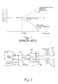
- a solid line 10 a plot indicating how the write head frequency response decreases as the frequency of the writing current increases when using a ferrite write head.
- the output for a given current has dropped significantly at the "roll off" frequency 120 which is, typically of the order 30 - 40 MHz and which limits a maximum write rate of the head to the order 80 MBits/s.
- the data pulses as written to the magnetic storage medium are convolved with the frequency response of the write head. This process of convolution has the effect of "smearing out” individual pulses on the storage medium.
- the smeared out pulses on the storage medium may overlap with the adjacent smeared out pulses as the pulse separation decreases. Eventually, the degree of overlap between adjacent pulses can become such that pulses cannot be distinguished during a read operation.
- the frequency response of the write head in a magnetic data storage device can act as a constraint on the highest frequencies and hence the highest data bit rates recorded to the magnetic data storage medium.
- any prior art attempts to boost high frequencies in such devices have been complex.
- Ampex produced a write pre-equalization scheme which comprised a current driver based on a linear amplifier, i.e. the output of the write driver was proportional to the input to the write driver.
- the Ampex scheme applied a boost to the high frequency response of the write driver to compensate for the roll-off in the frequency response of the write head.
- the Ampex implementation of write pre-equalization required substantial power, typically of the order 15 W, and could only be produced using discrete components and hence it was not possible to implement this as a single application specific integrated circuit (ASIC).
- ASIC application specific integrated circuit
- the Ampex scheme was also difficult to set up.
- positions of magnetic field transitions on a magnetic data storage medium may be laterally displaced with respect to one another dependent upon a time duration between a last positive going edge of the head driver current and a last going edge of a edge driver current.
- This lateral displacement of magnetization direction on the magnetic recording medium is also known herein as "bit shift", “peak shift” and “transition shift” is non-linear and is affected by the duration of at least the last driver current pulse.
- the ongoing pressure in the development of new magnetic data storage systems is to increase the data storage capacity of any magnetic data storage media.
- By increasing the effective bandwidth of the write head in a magnetic data storage system it is possible to increase the bit rate at which data are written to, for example, magnetic tapes and hence increasing the storage capacity of the tape.
- the specific embodiment and methods according to the present invention aim to increase the effective bandwidth of recording heads in magnetic data storage systems, and thereby increase the rate of which data can be written to magnetic data storage media in such systems.
- a data storage device for storing data signals, said device having a write channel characterized by comprising:
- said means for delaying said data signals has an adjustable delay time.
- said means for setting a relative amplitude of said data signals and said delayed data signals comprises:
- a said amplifier means may comprise an H-bridge electronic circuit.
- said means for amplifying said data signals and said means for amplifying said delayed data signals are configured such that a degree of amplification of said data signals relative to a degree of amplification of said delayed data signals is adjustable by means of at least one control signal.
- said first amplifier means and said second amplifier means are each independently controllable by a separate corresponding respective control signal.
- Said delay means may be capable of applying a variable delay period to said data signals.
- a degree of amplification of said data signals and a degree of amplification of said delayed data signals may be adjustable such that an amplitude of the amplified said data signals is larger than an amplitude of the amplified said delayed data signals.
- Said write head suitably comprises a magnetic recording head.
- said compensation means comprises an application specific integrated circuit.
- a method of writing data to a data storage medium via a write head comprising the steps of:
- Said data storage medium may comprise an elongate tape, and said write operation may comprise writing said modified data write signals along a length of said tape.
- a write head in a data storage device comprising the steps of:
- Said data signal from said host data source may be amplified to a first peak amplitude
- said delayed data signal is inverted with respect to said data signal
- said modified data write signal comprises a plurality of bits of information, each bit represented by a corresponding bit pulse comprising:
- the best mode herein relates to a Digital Data Storage system (DDS) based on the known digital audio tape system (DAT) being a helical scan system.
- DDS Digital Data Storage system
- DAT digital audio tape system
- the tape data storage system presented herein may advantageously implement one particular version of the DDS system namely the DDS4 standard which is still under development.
- the methods and apparatus disclosed herein are not restricted to systems having rotating heads or to systems where digital data are stored on tape.
- the generality of the present invention described herein is limited in scope only by the essential features according to the claims herein.
- FIGs. 2 to 4 there is illustrated schematically a write channel of a data storage device which records digital data onto a magnetic tape media using two write heads mounted on a rotating drum. Whilst a pair of write heads are presented in the best mode contemplated by the inventors, in general the methods presented herein apply to one or a plurality of write heads.
- the write head has a frequency response similar to that shown as line 110 in Fig. 1 herein, in which there is a degraded frequency response of the write head at higher frequencies.
- a channel ASIC 200 provides a source of logic signals which are to be recorded on to a tape according to the best mode presented herein.
- the channel ASIC 200 converts a stream of digital data from the host device into streams of digital data write signals 206 and 207 with appropriate voltage levels, to input into a write driver 201.
- Data stream 207 is an inverted version of data stream 206.
- the write driver 201 operates to modify bits of data comprising the data stream, boosting a higher frequency content of the data stream to fully or partially compensate for the higher frequency roll-off of the write heads.
- the process of inverting a digital signal comprises replacing every instance of the digital signal which represents binary digit "0" with a digital signal that represents binary digit "1” and replacing every instance of the digital signal which represents a binary digit "1" with a digital signal representing binary digit "0".
- the voltage levels output by channel ASIC 200 conform to the voltage levels conventionally used in known pseudo emitter coupled logic (PECL).
- the two logic states are typically represented by a differential voltage swing of 1V peak-to-peak.
- PECL has, typically, the same differential voltage swings as conventional emitter coupled logic (ECL) but have been translated by +5V.
- PECL is a well known way of transferring logic signals where the timing of such signals is critical.
- the voltage write signals 206 and 207 are input to the double pulse write driver 201.
- the write driver 201 outputs conventional write current signals set by external reference currents 210 and 211.
- Each bit pulse of write currents 212 and 213 output from write driver 201 have an extra narrow pulse of current added on each transition according to one aspect of the present invention.
- the width of this narrow current pulse is set by an extemal reference current and an extemal resistor or capacitor.
- the write current 212 and 213 are input to a multiplexor 202 which switches the write current between the two write heads 204 and 205 via a parasitic coupling 203 and transformers 208 and 209.
- the parasitic coupling 203 comprises a parasitic connection between the physical location of the double pulse write driver as described herein and either the transformers 208 and 209 or the write heads 204 and 205.
- Main driver current 301 is produced by a first transconductor circuit 400 which produces two write output signals in response to two input signals.
- the output signals of the first transconductor 400 are amplified versions of the write signals 206 and 207 input into first transconductor 400.
- the input signals are also input to a delay unit 402, the outputs of the delay unit being input to a second transconductor 401.
- Write signals 206, 207 input to first and second transconductors respectively each comprise a digital logic voltage signal. Outputs of the first and second transconductors comprise current signals.
- Each transconductor comprises a buffer, a switch, and a current amplifier source, the combination of buffer, switch and current amplifier source operating to receive a said voltage logic signal and output said a current pulse drive signal of predetermined and controlled current value.
- To the main driver current 301 is added an inverted and delayed driver current 302.
- the amplitude of the pulses in the driver current and delayed current are represented in Fig. 3 herein as IH and IH-pulse, respectively.
- the amplitudes of main driver current 301 and delayed inverted current 302 IH and IH-Pulse are respectively set by the reference currents 210 and 211 and may be preset.
- the main driver current 301 and delayed inverted current 302 are added to produce a modified write signal 212, denoted as sum (head) current in Fig. 3.
- the effect of adding the delayed inverted current 302 to main driver 301, if IH-pulse is less than IH, is to produce a respective double pulse current spike corresponding to each transition of the main driver current.
- the double pulse comprises a narrow pulse spike which has a positive leading edge which is coincident with the positive leading edge of the main driver current followed by a pulse having a lower amplitude than the a pulse of the main driver current, but being of longer duration. At each negative going leading edge of the main driver current there is a coincident negative going narrow pulse in the sum current.
- the positive going and negative going narrow pulse spikes are of the same duration as each other. Taking the Fourier transform of the narrow pulse spikes and broad main pulse components of the sum head current 212 it will be understood that the narrow pulse contributes significantly to the high frequency components of the resultant modified write signal, sum (head) current 212.
- the frequency spectral distribution of the modified write current input to the write head including additional high frequency components from the narrow pulse approximate to the frequency spectrum of a conventional write current having uniform amplitude over a wide range of frequencies multiplied by the dashed curve 130 shown in Fig. 1. These additional high frequency components in the write current partially compensate for the higher frequency roll-off in the frequency response of the write head at approximately 40 MHz.
- the additional high frequency components added to the write current results in an improved effective bandwidth of the write heads, and as a result may increase the roll off in the response of the write channel as a whole, including the write head, from approximately 40 MHz up to approximately 60MHz.
- Incorporation of a double pulse driver circuit in the write channel of a data storage device as described herein has the further advantage that it may be optimized such that a changing magnetic field generated by a record head in response to a positive going edge of a driver current rises to a same value irrespective of a time duration of a driver current pulse initiating the changing magnetic fields. Ensuring that the magnetic field rises to a fixed value irrespective of the duration of the driver current pulse initiating the rise in magnetic field reduces the occurrence of lateral displacement of changes in magnetization direction on the data storage medium. Minimizing relative lateral displacements between pulses recorded on a magnetic data storage medium minimizes the occurrence of timing errors during subsequent read operation and thereby minimizes the measured bit error rate.
- the write driver 201 and multiplexer 202 are implemented on a single application specific integrated circuit (ASIC).
- ASIC application specific integrated circuit
- the two logical signals WriteP 206 and WriteN 207 from Channel ASIC 200, are written to first transconductor 400.
- signals writeP 206 and writeN 207 are written to delay unit 402.
- the delay circuit stores and delays write signals 206 and 207 for a relatively short period of time. The delay period is designed to be easily adjustable and calibrated by changing the value of a single resistor or capacitance external to the ASIC.
- the optimal time by which the write signals should be delayed is found to be of the order of 3.5 ns.
- the delayed signals are written to second transconductor 401.
- transconductors 400 and 401 have substantially similar properties.
- First and second transconductors 400 and 401 are both conventional.
- the electronic circuitry comprising first transconductor 400 is preferably a direct copy of the electronic circuitry comprising second transconductor 401.
- the delayed logical signals are read out from second transconductor 401 and are combined with the output of first transconductor 400 prior to sending to write multiplexer 202.
- the output signals of second transconductor 401 and first transconductor 400 are combined in the following manner.
- the main driver current 301 is added to inverted delayed driver current 302 and inverted main driver current 405 is added to an inverted delayed version of itself, yielding the respective sum currents 202 and 213 which are used to drive the write heads.
- the sum current 212 and its inverted counterpart 213 are written to the write multiplexer 202.
- the write multiplexer switches the sum currents 212 and 213 between two write heads according to switching signals 408.
- Write current 212 is switched between inputs WHAP and WHBP which correspond to the two write heads 204 and 205.
- write signals 213 are switched between inputs WHAN and WHBN. Whilst a write channel serving two write heads is shown in the best mode herein, the invention applies equally to a write channel having a single write head, or any other plurality of write heads.
- the amplitudes of the main driver currents 301 and 405 and the delayed driver currents 406 and 302 which are combined before sending to the write heads are set by reference current IW x K1 and IW-Pulse X K2.
- K 1 and K 2 are chosen to ensure that main driver currents 301 and 405 have larger amplitudes than the delayed currents 406 and 302.
- FIG. 7 there is illustrated schematically a signal processing diagram for processing of the host data signals into a form which includes frequency components which compensate for a higher frequency roll off of the ferrite write head.
- Incoming host data signals in the form of bit pulses are split into first and second signal paths, the first path being amplified/buffered in first transconductor 400 by a first degree of amplification 700.
- the second signal path of host data signals is delayed by delay device 402 for a predetermined delay period, which may be varied by adjustment.
- the delayed host data signals are amplified/buffered in second transconductor 401, which also inverts the delayed host data signals and amplifies the host data signals by a second degree of amplification, the second degree of amplification being less than the first degree of amplification.
- the inverted delayed data signals are summed 704 with the amplified host data signal to produce a modified write signal as illustrated by sum (head) current 212 in Fig. 3 herein.
- the modified write signal is of the form described hereinabove, containing a relatively short higher amplitude spike on a leading edge of each main pulse, which introduces higher frequency components which compensate for a higher frequency roll off of the write head.
- the modified data write signal is written to the tape data storage medium via the write head 705.
- the resultant data signals written to the tape data storage medium may be better defined and have a better signal to noise ratio and/or a lower bit error rate than in the prior art case.
Landscapes
- Digital Magnetic Recording (AREA)
Priority Applications (1)
| Application Number | Priority Date | Filing Date | Title |
|---|---|---|---|
| EP99303792A EP0959469A1 (de) | 1998-05-19 | 1999-05-14 | Doppelpuls-Schreibtreiber |
Applications Claiming Priority (3)
| Application Number | Priority Date | Filing Date | Title |
|---|---|---|---|
| EP98303940A EP0959468A1 (de) | 1998-05-19 | 1998-05-19 | Doppelimpulsschreibtreiber |
| EP98303940 | 1998-05-19 | ||
| EP99303792A EP0959469A1 (de) | 1998-05-19 | 1999-05-14 | Doppelpuls-Schreibtreiber |
Publications (1)
| Publication Number | Publication Date |
|---|---|
| EP0959469A1 true EP0959469A1 (de) | 1999-11-24 |
Family
ID=26151270
Family Applications (1)
| Application Number | Title | Priority Date | Filing Date |
|---|---|---|---|
| EP99303792A Withdrawn EP0959469A1 (de) | 1998-05-19 | 1999-05-14 | Doppelpuls-Schreibtreiber |
Country Status (1)
| Country | Link |
|---|---|
| EP (1) | EP0959469A1 (de) |
Citations (5)
| Publication number | Priority date | Publication date | Assignee | Title |
|---|---|---|---|---|
| US5333081A (en) * | 1991-09-27 | 1994-07-26 | Nec Corporation | Magnetic head driving circuit with delay elements between the switching components |
| US5339202A (en) * | 1993-03-26 | 1994-08-16 | Minnesota Mining And Manufacturing Company | Method and apparatus for amplitude compensated write equalization |
| US5392172A (en) * | 1992-01-30 | 1995-02-21 | Hitachi, Ltd. | Magnetic head circuit having a write current changeover circuit with a clamp voltage depending on write current for high-speed data transfer |
| US5550502A (en) * | 1995-05-23 | 1996-08-27 | Gec Plessey Semiconductors, Inc. | Control circuit and method for thin film head writed river |
| JPH09259404A (ja) * | 1996-03-22 | 1997-10-03 | Sony Corp | ライト電流発生回路 |
-
1999
- 1999-05-14 EP EP99303792A patent/EP0959469A1/de not_active Withdrawn
Patent Citations (5)
| Publication number | Priority date | Publication date | Assignee | Title |
|---|---|---|---|---|
| US5333081A (en) * | 1991-09-27 | 1994-07-26 | Nec Corporation | Magnetic head driving circuit with delay elements between the switching components |
| US5392172A (en) * | 1992-01-30 | 1995-02-21 | Hitachi, Ltd. | Magnetic head circuit having a write current changeover circuit with a clamp voltage depending on write current for high-speed data transfer |
| US5339202A (en) * | 1993-03-26 | 1994-08-16 | Minnesota Mining And Manufacturing Company | Method and apparatus for amplitude compensated write equalization |
| US5550502A (en) * | 1995-05-23 | 1996-08-27 | Gec Plessey Semiconductors, Inc. | Control circuit and method for thin film head writed river |
| JPH09259404A (ja) * | 1996-03-22 | 1997-10-03 | Sony Corp | ライト電流発生回路 |
Non-Patent Citations (1)
| Title |
|---|
| PATENT ABSTRACTS OF JAPAN vol. 098, no. 002 30 January 1998 (1998-01-30) * |
Similar Documents
| Publication | Publication Date | Title |
|---|---|---|
| US4314289A (en) | Biased pulsed recording systems and methods | |
| US7589649B1 (en) | Apparatus, method, and system for correction of baseline wander | |
| CN1661706A (zh) | 使用读取定时路径提供写入预补偿的方法及设备 | |
| EP1393437A2 (de) | Verfahren und durchführung zur verzerrungskompensation zweiter ordnung | |
| US6307692B1 (en) | Double pulse write driver | |
| US7755522B1 (en) | Apparatus, method, and circuit for baseline loop analog cancellation | |
| US6172832B1 (en) | Data storage system with improved biasing techniques for magneto-resistive element | |
| US6256158B1 (en) | Calibrating write pre-equalization in a data storage device | |
| CN1140895C (zh) | 存储装置 | |
| JP2003517695A (ja) | デジタル非対称読取り信号を修正する方法及び装置 | |
| JP3761329B2 (ja) | 記憶装置 | |
| EP0959470B1 (de) | Kalibrierung der Schreib-Vorentzerrung in einer Datenspeicheranordnung | |
| JPH01159808A (ja) | 2進ディジタル信号再生装置 | |
| KR19990022109A (ko) | 디스크 드라이브용 공진 동조를 위한 적응 전치 증폭기 | |
| CN1661705A (zh) | 提供普适写入预补偿的方法及设备 | |
| US6229950B1 (en) | Reproducing apparatus capable of controlling reproduction equalizing characteristic | |
| JP3600311B2 (ja) | 磁気記録再生装置 | |
| JP3087860B2 (ja) | 磁気記憶装置の記録回路 | |
| Bellis | Introduction to digital audio recording | |
| JPH11328926A (ja) | 磁気記録再生装置 | |
| EP1411501A1 (de) | Magnetische wiedergabevorrichtung und magnetisches wiedergabeverfahren | |
| JPH09102102A (ja) | 磁気ディスク装置 | |
| JPH05135309A (ja) | 磁気記録装置 | |
| JPH11203608A (ja) | 記録等化器およびそれを用いた磁気記録再生装置 | |
| JPH01271972A (ja) | 垂直磁気記録再生波形等化器 |
Legal Events
| Date | Code | Title | Description |
|---|---|---|---|
| PUAI | Public reference made under article 153(3) epc to a published international application that has entered the european phase |
Free format text: ORIGINAL CODE: 0009012 |
|
| AK | Designated contracting states |
Kind code of ref document: A1 Designated state(s): DE FR GB NL |
|
| AX | Request for extension of the european patent |
Free format text: AL;LT;LV;MK;RO;SI |
|
| 17P | Request for examination filed |
Effective date: 20000512 |
|
| AKX | Designation fees paid |
Free format text: DE FR GB NL |
|
| RAP1 | Party data changed (applicant data changed or rights of an application transferred) |
Owner name: HEWLETT-PACKARD COMPANY, A DELAWARE CORPORATION |
|
| 17Q | First examination report despatched |
Effective date: 20030505 |
|
| GRAP | Despatch of communication of intention to grant a patent |
Free format text: ORIGINAL CODE: EPIDOSNIGR1 |
|
| STAA | Information on the status of an ep patent application or granted ep patent |
Free format text: STATUS: THE APPLICATION IS DEEMED TO BE WITHDRAWN |
|
| 18D | Application deemed to be withdrawn |
Effective date: 20051222 |