EP0955602A1 - Non-contact ic card - Google Patents
Non-contact ic card Download PDFInfo
- Publication number
- EP0955602A1 EP0955602A1 EP98900202A EP98900202A EP0955602A1 EP 0955602 A1 EP0955602 A1 EP 0955602A1 EP 98900202 A EP98900202 A EP 98900202A EP 98900202 A EP98900202 A EP 98900202A EP 0955602 A1 EP0955602 A1 EP 0955602A1
- Authority
- EP
- European Patent Office
- Prior art keywords
- data
- storing
- state
- storing means
- location
- Prior art date
- Legal status (The legal status is an assumption and is not a legal conclusion. Google has not performed a legal analysis and makes no representation as to the accuracy of the status listed.)
- Granted
Links
Images




Classifications
-
- G—PHYSICS
- G07—CHECKING-DEVICES
- G07F—COIN-FREED OR LIKE APPARATUS
- G07F7/00—Mechanisms actuated by objects other than coins to free or to actuate vending, hiring, coin or paper currency dispensing or refunding apparatus
- G07F7/08—Mechanisms actuated by objects other than coins to free or to actuate vending, hiring, coin or paper currency dispensing or refunding apparatus by coded identity card or credit card or other personal identification means
- G07F7/10—Mechanisms actuated by objects other than coins to free or to actuate vending, hiring, coin or paper currency dispensing or refunding apparatus by coded identity card or credit card or other personal identification means together with a coded signal, e.g. in the form of personal identification information, like personal identification number [PIN] or biometric data
- G07F7/1008—Active credit-cards provided with means to personalise their use, e.g. with PIN-introduction/comparison system
-
- G—PHYSICS
- G06—COMPUTING OR CALCULATING; COUNTING
- G06K—GRAPHICAL DATA READING; PRESENTATION OF DATA; RECORD CARRIERS; HANDLING RECORD CARRIERS
- G06K19/00—Record carriers for use with machines and with at least a part designed to carry digital markings
- G06K19/06—Record carriers for use with machines and with at least a part designed to carry digital markings characterised by the kind of the digital marking, e.g. shape, nature, code
- G06K19/067—Record carriers with conductive marks, printed circuits or semiconductor circuit elements, e.g. credit or identity cards also with resonating or responding marks without active components
- G06K19/07—Record carriers with conductive marks, printed circuits or semiconductor circuit elements, e.g. credit or identity cards also with resonating or responding marks without active components with integrated circuit chips
- G06K19/073—Special arrangements for circuits, e.g. for protecting identification code in memory
-
- G—PHYSICS
- G06—COMPUTING OR CALCULATING; COUNTING
- G06Q—INFORMATION AND COMMUNICATION TECHNOLOGY [ICT] SPECIALLY ADAPTED FOR ADMINISTRATIVE, COMMERCIAL, FINANCIAL, MANAGERIAL OR SUPERVISORY PURPOSES; SYSTEMS OR METHODS SPECIALLY ADAPTED FOR ADMINISTRATIVE, COMMERCIAL, FINANCIAL, MANAGERIAL OR SUPERVISORY PURPOSES, NOT OTHERWISE PROVIDED FOR
- G06Q20/00—Payment architectures, schemes or protocols
- G06Q20/08—Payment architectures
- G06Q20/10—Payment architectures specially adapted for electronic funds transfer [EFT] systems; specially adapted for home banking systems
- G06Q20/105—Payment architectures specially adapted for electronic funds transfer [EFT] systems; specially adapted for home banking systems involving programming of a portable memory device, e.g. IC cards, "electronic purses"
-
- G—PHYSICS
- G06—COMPUTING OR CALCULATING; COUNTING
- G06Q—INFORMATION AND COMMUNICATION TECHNOLOGY [ICT] SPECIALLY ADAPTED FOR ADMINISTRATIVE, COMMERCIAL, FINANCIAL, MANAGERIAL OR SUPERVISORY PURPOSES; SYSTEMS OR METHODS SPECIALLY ADAPTED FOR ADMINISTRATIVE, COMMERCIAL, FINANCIAL, MANAGERIAL OR SUPERVISORY PURPOSES, NOT OTHERWISE PROVIDED FOR
- G06Q20/00—Payment architectures, schemes or protocols
- G06Q20/30—Payment architectures, schemes or protocols characterised by the use of specific devices or networks
- G06Q20/34—Payment architectures, schemes or protocols characterised by the use of specific devices or networks using cards, e.g. integrated circuit [IC] cards or magnetic cards
- G06Q20/341—Active cards, i.e. cards including their own processing means, e.g. including an IC or chip
-
- G—PHYSICS
- G06—COMPUTING OR CALCULATING; COUNTING
- G06Q—INFORMATION AND COMMUNICATION TECHNOLOGY [ICT] SPECIALLY ADAPTED FOR ADMINISTRATIVE, COMMERCIAL, FINANCIAL, MANAGERIAL OR SUPERVISORY PURPOSES; SYSTEMS OR METHODS SPECIALLY ADAPTED FOR ADMINISTRATIVE, COMMERCIAL, FINANCIAL, MANAGERIAL OR SUPERVISORY PURPOSES, NOT OTHERWISE PROVIDED FOR
- G06Q20/00—Payment architectures, schemes or protocols
- G06Q20/30—Payment architectures, schemes or protocols characterised by the use of specific devices or networks
- G06Q20/34—Payment architectures, schemes or protocols characterised by the use of specific devices or networks using cards, e.g. integrated circuit [IC] cards or magnetic cards
- G06Q20/357—Cards having a plurality of specified features
Definitions
- the present invention relates to a non contact type IC card, and more particularly to a non contact type IC card allowing the protection of data stored in the card and the prevention of data falsification.
- a non contact type IC card performing data communication with an interrogator installed outside has been used conventionally.
- the examples include a ticket for ski lift, a seasonal ticket for the transportation and a prepaid card.
- Fig. 7 is a block diagram schematically showing a basic structure of a conventional non contact type IC card 900.
- Conventional non contact type IC card 900 shown herein which is an IC card performing data communication in a signal superposing manner, supplies power and transmits/receives information using a signal(s) having one or more frequencies received from the interrogator not shown.
- Conventional non contact type IC card 900 as shown in Fig. 7 is an example of non contact type IC cards utilizing a single frequency and includes a tuning circuit 20, a rectifying circuit 21, an amplifying/demodulating circuit 22, a modulating/amplifying circuit 23 and an SP/PS conversion circuit 24.
- Tuning circuit 20 includes a coil L functioning as an antenna and a capacitor C0.
- Rectifying circuit 21 rectifies a signal received at tuning circuit 20, thereby generates and supplies the power to each part of non contact type IC card 900.
- Amplifying/demodulating circuit 22 amplifies and demodulates data Q from an interrogator received at tuning circuit 20.
- a signal output from amplifying/demodulating circuit 22 is SP-converted by SP/PS conversion circuit 24 and then is output to a main control circuit 2 described below.
- conventional non contact type IC card 900 further includes main control circuit 2 and a memory 1.
- Main control circuit 2 processes a signal output from SP/PS conversion circuit 24.
- Main control circuit 2 generates data DA to be stored in memory 1 described below and designates a location (address) of memory 1 to which data DA is to be written.
- Memory 1 includes normal data storage region B1 and data protection region B2.
- Memory 1 receives data DA via a data line L2 as well as an address signal AD via an address line L1 indicating an address (a location to which data is to be written) to which data DA is to be written.
- data stored in data protection region B2 particularly requires security in order to guarantee a normal data communication and whose rewriting is inhibited.
- An example of such data is an ID number of an ID card holding the personal information.
- main control circuit 2 reads data from designated region B1 or data protection region B2 of memory 1 according to the contents of data Q received from the interrogator and generates a response data A based on the read data.
- Response data A is PS-converted at SP/PS conversion circuit 24, processed at modulating/amplifying circuit 23 and then transmitted to the interrogator via coil L forming the antenna.
- an object of the present invention is to provide a non contact type IC card allowing the prevention of rewriting of a storage region in which data requiring security is stored.
- Another object of the present invention is to provide a highly reliable non contact type IC card through the control of rewriting of the storage region in which data requiring security is stored.
- a non contact type IC card is responsive to externally applied data for performing data communication, and includes: a first storing circuit storing data requiring security; a second storing circuit storing data other than the data to be stored in the first storing circuit; a control circuit controlling for writing the data into a location in one of the first storing circuit and the second storing circuit according to a content of the data; a selection circuit selecting whether the data is to be written into the location in the first storing circuit designated by the control circuit; and a state setting circuit controlling the selection by the selection circuit, the data is written into the location in the first storing circuit designated by the control circuit when the state setting circuit is in a first state, whereas, the data is inhibited from being written into the first storing circuit designated by the control circuit when the state setting circuit is in a second state other than the first state.
- a non contact type IC card is responsive to externally applied data for performing data communication, and includes: a first storing circuit storing the data requiring security; a second storing circuit storing data other than the data to be stored in the first storing circuit; a control circuit controlling for writing the data into a location in one of the first storing circuit and the second storing circuit according to a content of the data; a detection circuit receiving a control signal from the control circuit and giving instruction for controlling a state of the first storing circuit; and a selection circuit receiving the instruction of the detection circuit and selecting whether the data is to be written into the location of the first storing circuit designated by the control circuit; and the control signal output from the control circuit indicates whether the first storing circuit is in a data rewriting permitted state or a data rewriting inhibited state; and the data is written into the location in the first storing circuit designated by the control circuit when the detection circuit detects that the first storing circuit is in the data rewriting permitted state, whereas the data is not written into
- a non contact type IC card performs a data communication based on an externally applied radio wave signal, and includes: a receiving circuit receiving the radio wave signal; a first storing circuit storing the data requiring security; a second storing circuit storing data other than the data to be stored in the first storing circuit; a control circuit generating the data based on the radio wave signal received at the receiving circuit and controlling for writing the data into a location in one of the first storing circuit and the second storing circuit according to a content of the generated data; a detection circuit detecting a frequency of the radio wave signal received by the receiving circuit; and a selection circuit selecting whether the data is to be written into the location in the first storing circuit designated by the control circuit based on a result of the detection by the detection circuit; and wherein the data is written into the location in the first storing circuit designated by the control circuit, when the receiving circuit receives the radio wave signal and the frequency of the radio wave signal is detected to be a first frequency by the detection circuit, whereas the
- a non contact type IC card is responsive to externally applied data for performing data communication, and includes: a first storing circuit storing the data requiring security; a second storing circuit storing data other than the data to be stored in the first storing circuit; a control circuit controlling for writing the data into a location in one of the first storing circuit and the second storing circuit according to a content of the data; and a data fixing circuit receiving the data to be written into the location in the first storing circuit designated by the control circuit and supplying a particular data; and wherein a value of the predetermined data supplied from the data fixing circuit is a value determined by an initial state of the first storing circuit, and wherein only the particular data supplied from the data fixing circuit is written into the location in the first storing circuit designated by the control circuit.
- a non contact type IC card is responsive to externally applied data for performing data communication, and includes: a first storing circuit storing said data requiring security; a second storing circuit storing data other than the data to be stored in the first storing circuit; a control circuit controlling for writing the data into a location in one of the first storing circuit and the second storing circuit according to a content of the data; a selection circuit selecting whether the data is to be written into the location in the first storing circuit designated by the control circuit; and a state setting circuit controlling the selection by the selection circuit; and wherein the data is written into the location in the first storing circuit designated by the control circuit when the state setting circuit is in a first state, whereas, the data is written into a location other than the location in the first storing circuit designated by the control circuit when the state setting circuit is in a second state other than the first state.
- a non contact type IC card is responsive to externally applied data for performing data communication, and includes: a first storing circuit storing the data requiring security; a second storing circuit storing data other than the data to be stored in the first storing circuit; and a control circuit controlling for writing the data into a location in one of the first storing circuit and the second storing circuit according to a content of the data; and wherein the first storing circuit allows rewriting of a predetermined times.
- a main advantage of the present invention lies in the prevention of falsification of storage contents through the control of rewriting of data stored in a storage portion storing data requiring security.
- the first embodiment of the present invention allows the prevention of rewriting of data previously stored in a data protection region by controlling an address to which data is to be written, at data writing for the data protection region of a memory in a non contact type IC card.
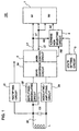
- Fig. 1 shows a structure of a main portion of a non contact type IC card 100 according to the first embodiment of the present invention.
- Components similar to those in conventional non contact type IC card 900 shown in Fig. 7 are denoted by the same reference numbers and same reference characters and the description thereof will not be repeated.
- data transmission of the non contact type IC card adopting the present invention may be either in a signal superposing method or in a signal separating method.
- Non contact type IC card 100 shown in Fig. 1 differs from conventional non contact type IC card 900 in that card 100 includes a state setting circuit 3 and an address non selecting circuit 4 controlling a write address designated at data writing for data protection region B2 of memory 1.
- non contact type IC card 100 With reference to Fig. 1, the structure of non contact type IC card 100 according to the first embodiment of the present invention will be described.
- Address non selecting circuit 4 receives a write enable signal RE supplied from main control circuit 2 and an address signal AD from an address line L1 as inputs.
- address signal AD designates a location in data protection region B2 to which data DT on a data line L2 is to be written
- write enable signal RE designates a data writing operation to data protection region B2.
- Address non selecting circuit 4 being controlled by state setting circuit 3 described below outputs an address selecting signal AC according to address signal AD.
- State setting circuit 3 controls address non selecting circuit 4 described above.
- Address selecting signal AC output from address non selecting circuit 4 changes its state based on a state (active state/inactive state) of state setting circuit 3. Specifically, when state setting circuit 3 is in an active state, an output address selecting signal AC selects a location designated by address AD as a location to which data is to be written, whereas when state setting circuit 3 is in an inactive state, an output address selecting signal AC inhibits the writing to the location designated by address signal AD (non select state).
- Data DT will be written into a location in data protection region B2 corresponding to and based on address selecting signal AC output from address non selecting circuit 4.
- address non selecting circuit 4 when state setting circuit 3 is in an active state, address non selecting circuit 4 having received write enable signal RE and address signal AD outputs address selecting signal AC selecting a location designated by the address signal AD. In this case data DT will be written into the corresponding location in data protection region B2.
- address non selecting circuit 4 when stage setting circuit 3 is in an inactive state, address non selecting circuit 4 having received write enable signal RE and address signal AD outputs address selecting signal AC turning the location designated by the address signal AD to a non select state. In this case data DT is not written into data protection region B2.
- Such state setting circuit 3 uses a fuse.
- a fuse when a fuse is used, any numbers of data can be written into data protection region B2 before the fuse blow, however, after the fuse blow, data in data protection region B2 can not be rewritten.
- the methods of blowing the fuse includes high voltage application, laser cutting, induction heating or the like.
- non contact type IC card 100 can inhibit the access to data protection region B2 for data rewriting after the data requiring security is stored in data protection region B2 (for simplicity this state is referred to as protection data storage state).
- non contact type IC card 100 as the address selection for the data protection region can be controlled at the data writing operation, the falsification of data previously stored in the data protection region can be prevented.
- the non contact type IC card according to the second embodiment of the present invention allows the prevention of rewriting of data stored in the data protection region by controlling an address to which the data is to be written at the time of data writing to the data protection region in the memory.
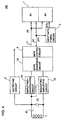
- Fig. 2 shows a structure of a main portion of a non contact type IC card 200 according to the second embodiment of the present invention and components similar to those in non contact type IC card 100 shown in Fig. 1 are denoted by the same reference numbers and same reference characters and the description thereof will not be repeated.
- Non contact type IC card 200 shown in Fig. 2 is different from conventional non contact type IC card 900 in that it includes a command detection circuit 5 and an address non selecting circuit 6 controlling a designated address to which data is to be written at the time of data writing to the data protection region of the memory, and controls these circuits by a command output from a main control circuit 12.
- non contact type IC card 200 With reference to Fig. 2, the structure of non contact type IC card 200 according to the second embodiment of the present invention will now be described.
- Address non selecting circuit 6 receives an address signal AD via an address line L1 as an input.
- address signal AD indicates a location in data protection region B2 to which data DT on a data line L2 is to be written.
- Address non selecting circuit 6 controlled by command detection circuit 5 described below outputs address selecting signal AC according to the address signal AD.
- Command detection circuit 5 receives an address control command COM output from main control circuit 12 and controls address non selecting circuit 6.
- address control command COM is a command permitting or inhibiting a data writing operation to data protection region B2 based on the address signal AD.
- Address selecting signal AC output from address non selecting circuit 6 changes its state according to a state of command detection circuit 5. Specifically, when command detection circuit 5 detects a writing permitted state of a data protection region B2, an address selecting signal AC selecting a location designated by address AD as a location to which data is to be written is output. On the other hand, if data protection region B2 is detected to be in a writing inhibited state, address selecting signal AC turning a location designated by address signal AD to a non select state is output.
- data DT is written into a corresponding location in data protection region B2.
- address non selecting circuit 6 When an address control command COM permitting the data writing is supplied from main control circuit 12, and is detected by command detection circuit 5, address non selecting circuit 6 outputs an address selecting signal AC selecting a location designated by the address signal AD. In this case data DT is written into a corresponding location in data protection region B2.
- address non selecting circuit 6 outputs an address selecting signal AC turning the location designated by the address signal AD to a non select state. In this case data DT is not written into data protection region B2.
- non contact type IC card 200 allows the adjustment of storage of data requiring security in data protection region B2 (turning data protection region B2 to the protection data storage state) and inhibiting the access to data protection region B2 for the data rewriting, through the control of command detection circuit 5 based on a command output from main control circuit 12.
- non contact type IC card 200 allows the control of selection of address of the data protection region at the data writing operation, the falsification of data previously stored in the data protection region can be prevented.
- the third embodiment of the present invention allows the prevention of rewriting of data once stored in the data protection region in the non contact type IC card through the access control for the data protection region according to the frequency for data communication.
- Fig. 3 shows a structure of a main portion of a non contact type IC card 300 according to the third embodiment of the present invention, wherein components similar to those in non contact type IC card 100 shown in Fig. 1 are denoted by the same reference numbers and same reference characters, and the description thereof will not be repeated.
- Non contact type IC card 300 shown in Fig. 3 is different from conventional non contact type IC card 900 in that it includes a frequency detection circuit 7 and an address non selecting circuit 8.
- non contact type IC card 300 With reference to Fig. 3, the structure of non contact type IC card 300 according to the third embodiment of the present invention will now be described.
- Frequency detection circuit 7 detects a frequency of a radio wave received by tuning circuit 20 and includes a band pass filter and a switching circuit inside not shown. When a carrier frequency of a received radio wave is a predetermined frequency F1, frequency detection circuit 7 detects the reception of an intended radio wave.
- Address non selecting circuit 8 receives address signal AD via address Line L1 and a write enable signal RE from main control circuit 2 as inputs.
- address signal AD designates a location in data protection region B2 to which data DT on data line L2 is to be written.
- Address non selecting circuit 8 controlled by frequency detection circuit 7 outputs address selecting signal AC according to address signal AD. More specifically, when frequency detection circuit 7 detects the reception of an intended radio wave (with predetermined frequency F1), an address selecting signal AC selecting a location designated by address signal AD as a location to which data is to be written is output, and otherwise (when received radio wave has a frequency other than the predetermined frequency F1), an address selecting signal AC turning the location designated by the address signal AD to a non select state is output.
- non contact type IC card 300 With reference to Fig. 3, an operation of non contact type IC card 300 will be described specifically.
- address non selecting circuit 8 when a radio wave with a carrier frequency F1 is received, address non selecting circuit 8 outputs an address selecting signal AC selecting a location designated by address signal AD. In this case data DT is written into the corresponding location in data protection region B2.
- address non selecting circuit 8 when a radio wave with a carrier frequency being an original frequency F0 different from F1 is received, address non selecting circuit 8 outputs an address selecting signal AC turning the location designated by address signal AD to a non select state. In this case data DT is not written into data protection region B2.
- non contact type IC card 300 allows the adjustment of the storage of data requiring security in data protection region B2 (turning data protection region B2 to the protection data storage state) and inhibiting the access to data protection region B2 for the data rewriting, through the use of different frequencies.
- a non contact type IC card 300 allows the access control for the data protection region according to the frequency of radio wave for the data communication, the falsification of data previously stored in the data protection region can be prevented.
- the fourth embodiment of the present invention allows the prevention of data falsification, which is the object of the present invention, in the non contact type IC card by controlling the data to be written at the data writing to the data protection region in the memory.
- Fig. 4 shows a structure of a main portion of a non contact type IC card 400 according to the fourth embodiment of the present invention, wherein components similar to those in non contact type IC card 100 shown in Fig. 1 are denoted by the same reference numbers and same reference characters, and the description thereof will not be repeated.
- Non contact type IC card 400 shown in Fig. 4 is different from conventional non contact type IC card 900 in that it includes an input data fixing circuit 9 controlling data to be written into data protection region B2 of memory 1.
- non contact type IC card 400 With reference to Fig. 4, the structure of non contact type IC card 400 according to the fourth embodiment of the present invention will be described.
- Input data fixing circuit 9 fixes a state of each location in data protection region B2 of memory 1.
- Input data fixing circuit 9 receives data DT1 via a data line L2 as an input, converts data DT1 and outputs data DT2. Data DT2 is data to be written into data protection region B2.
- a value of data DT2 output from input data fixing circuit 9 is determined based on an initial state of data protection region B2.
- states of all bits in data protection region B2 are "1"
- data DT2 always takes a value of the reverse polarity, in this case "0”.
- main control circuit 2 outputs data DT1 corresponding to the value "1"
- the data writing to data protection region B2 will not be performed.
- non contact type IC card 400 With reference to Fig. 4, an operation of non contact type IC card 400 will be described specifically.
- data requiring security will be written into data protection region B2 (protection data storage state).
- the protection data storage state is "1100".
- data DT2 output from input data fixing circuit 9 takes the value "0". Therefore, the bit once takes the state "0" cannot be returned to the state "1". As a result, thereafter, the state of data protection region B2 ("1100") cannot be rewritten to "1101", for example.
- data protection region B2 of non contact type IC card 400 functions as an OTP ROM (a non volatile memory allowing only one rewriting) and once data is stored in the data protection region, trial of the data rewriting is highly likely to result in a failure of an intended data setting.
- OTP ROM a non volatile memory allowing only one rewriting
- non contact type IC card 400 allows the control of data to be written into the data protection region at the data writing operation, the rewriting of data once stored in the data protection region can be prevented.
- the fifth embodiment of the present invention allows the prevention of data falsification, which is the object of the present invention, in the non contact type IC card, by controlling an address to which data is to be written at the data writing operation to the data protection region of the memory.
- Fig. 5 shows a structure of a main portion of a non contact type IC card 500 according to the fifth embodiment of the present invention, wherein components similar to those in non contact type IC card 100 shown in Fig. 1 are denoted by the same reference numbers and same reference characters, and the description thereof will not be repeated.
- Non contact type IC card 500 shown in Fig. 5 is different from conventional non contact type IC card 900 in that it includes a state setting circuit 10 and an address non selecting circuit 11 controlling a designated address to which data is to be written at the writing to data protection region B2 of memory 1.
- non contact type IC card 500 With reference to Fig. 5, the structure of non contact type IC card 500 according to the fifth embodiment of the present invention will be described.
- Address non selecting circuit 11 receives a write enable signal RE output from main control circuit 2 and address signal AD via address line L1 as inputs.
- address signal AD designates a location in data protection region B2 to which data DT on data line L2 is to be written.
- State setting circuit 10 controls address non selecting circuit 11 described above.
- Address selecting signal AC output from address non selecting circuit 11 changes its state according to a state (active state/inactive state) of state setting circuit 10. More specifically, when state setting circuit 10 is in an active state, address selecting signal AC selecting a location designated by address signal AD as a location to which data is to be written is output, and when state setting circuit 10 is in an inactive state, address selecting signal AC selecting a location other than the location designated by address signal AD (or selecting neither of the location) is output.
- address non selecting circuit 11 having received write enable signal RE and address signal AD outputs an address selecting signal AC selecting a location designated by address signal AD.
- data DT is written into the corresponding location in data protection region B2.
- address non selecting circuit 11 when state setting circuit 10 is in an inactive state, address non selecting circuit 11 having received write enable signal RE and address signal AD outputs an address selecting signal AC selecting a location other than the location designated by address signal AD (or selecting neither of the locations). In this case, data DT is not written into the intended location of data protection region B2.
- an example of such state setting circuit 10 includes a fuse.
- non contact type IC card 500 can inhibit the rewriting of the intended data, after the data requiring security is stored in data protection region B2 (protection data storage state), by controlling the state of state setting circuit 10.
- non contact type IC card 500 allows the control of address selection in the data protection region at the data writing operation, rewriting and use of the data previously stored in the data protection region can be prevented.
- a non contact type IC card includes an OTP ROM (an non volatile memory allowing only one rewriting) as a storage medium corresponding to the data protection region.
- OTP ROM an non volatile memory allowing only one rewriting
- Fig. 6 shows a structure of a main portion of a non contact type IC card 600 according to the sixth embodiment of the present invention, wherein components similar to those in non contact type IC card 100 shown in Fig. 1 are denoted by the same reference characters and the description thereof will not be repeated.
- Non contact type IC card 600 shown in Fig. 6 is different from conventional non contact type IC card 900 in that it includes a memory 15 and a memory 16 instead of memory 1.
- non contact type IC card 600 With reference to Fig. 6, the structure of non contact type IC card 600 according to the sixth embodiment of the present invention will be described.
- Memory 15 is a storage medium storing rewritable data whereas memory 16 is a storage medium storing data requiring the security.
- memory 15 includes a non volatile memory allowing rewriting as required such as an EEPROM and a flash memory
- memory 16 includes a memory allowing only one rewriting such as an EPROM.
- non contact type IC card 600 Next, an operation of non contact type IC card 600 according to the sixth embodiment of the present invention will be described.
- memory 16 is assumed to be an EPROM.
- Data to be held that is output from main control circuit 2 is stored in memory 15 or memory 16.
- memory 16 is an EPROM
- the electric charge cannot be discharged until it is exposed to ultraviolet light. Therefore, assuming that the state of a memory cell with electric charge stored is called state 1 and the discharged state of the memory cell is called state 0, after the encapsulation of IC card 600, in memory 16, a memory cell in the state 0 can be charged to be the state 1, however, a memory cell in the state 1 cannot be rewritten to be the state 0.
- non contact type IC card 600 allows the suppression of data falsification to an extremely low level.
- the rewriting of storage region in which data requiring the security is stored can be prevented through the control of data rewriting.
- the reliability of the non contact type IC card can be dramatically improved.
Landscapes
- Engineering & Computer Science (AREA)
- Business, Economics & Management (AREA)
- General Physics & Mathematics (AREA)
- Physics & Mathematics (AREA)
- Accounting & Taxation (AREA)
- Theoretical Computer Science (AREA)
- Microelectronics & Electronic Packaging (AREA)
- Strategic Management (AREA)
- General Business, Economics & Management (AREA)
- Computer Networks & Wireless Communication (AREA)
- Computer Hardware Design (AREA)
- Finance (AREA)
- Computer Security & Cryptography (AREA)
- General Engineering & Computer Science (AREA)
- Development Economics (AREA)
- Economics (AREA)
- Storage Device Security (AREA)
- Credit Cards Or The Like (AREA)
Abstract
Description
- The present invention relates to a non contact type IC card, and more particularly to a non contact type IC card allowing the protection of data stored in the card and the prevention of data falsification.
- A non contact type IC card performing data communication with an interrogator installed outside has been used conventionally. The examples include a ticket for ski lift, a seasonal ticket for the transportation and a prepaid card.
- Fig. 7 is a block diagram schematically showing a basic structure of a conventional non contact
type IC card 900. Conventional non contacttype IC card 900 shown herein, which is an IC card performing data communication in a signal superposing manner, supplies power and transmits/receives information using a signal(s) having one or more frequencies received from the interrogator not shown. - Conventional non contact
type IC card 900 as shown in Fig. 7 is an example of non contact type IC cards utilizing a single frequency and includes atuning circuit 20, a rectifyingcircuit 21, an amplifying/demodulating circuit 22, a modulating/amplifyingcircuit 23 and an SP/PS conversion circuit 24. -
Tuning circuit 20 includes a coil L functioning as an antenna and a capacitor C0. Rectifyingcircuit 21 rectifies a signal received attuning circuit 20, thereby generates and supplies the power to each part of non contacttype IC card 900. - Amplifying/demodulating
circuit 22 amplifies and demodulates data Q from an interrogator received attuning circuit 20. A signal output from amplifying/demodulatingcircuit 22 is SP-converted by SP/PS conversion circuit 24 and then is output to amain control circuit 2 described below. - With reference to Fig. 7, conventional non contact
type IC card 900 further includesmain control circuit 2 and a memory 1. -
Main control circuit 2 processes a signal output from SP/PS conversion circuit 24.Main control circuit 2 generates data DA to be stored in memory 1 described below and designates a location (address) of memory 1 to which data DA is to be written. - Memory 1 includes normal data storage region B1 and data protection region B2. Memory 1 receives data DA via a data line L2 as well as an address signal AD via an address line L1 indicating an address (a location to which data is to be written) to which data DA is to be written. Here, data stored in data protection region B2 particularly requires security in order to guarantee a normal data communication and whose rewriting is inhibited. An example of such data is an ID number of an ID card holding the personal information.
- In addition,
main control circuit 2 reads data from designated region B1 or data protection region B2 of memory 1 according to the contents of data Q received from the interrogator and generates a response data A based on the read data. Response data A is PS-converted at SP/PS conversion circuit 24, processed at modulating/amplifyingcircuit 23 and then transmitted to the interrogator via coil L forming the antenna. - In conventional non contact
type IC card 900, however, the rewriting (falsification) of stored data in memory 1 can be easily performed from a device other than the interrogator once the protocol of the data communication with the interrogator is decoded, therefore the security cannot be guaranteed. - Hence an object of the present invention is to provide a non contact type IC card allowing the prevention of rewriting of a storage region in which data requiring security is stored.
- Another object of the present invention is to provide a highly reliable non contact type IC card through the control of rewriting of the storage region in which data requiring security is stored.
- A non contact type IC card according to the present invention is responsive to externally applied data for performing data communication, and includes: a first storing circuit storing data requiring security; a second storing circuit storing data other than the data to be stored in the first storing circuit; a control circuit controlling for writing the data into a location in one of the first storing circuit and the second storing circuit according to a content of the data; a selection circuit selecting whether the data is to be written into the location in the first storing circuit designated by the control circuit; and a state setting circuit controlling the selection by the selection circuit, the data is written into the location in the first storing circuit designated by the control circuit when the state setting circuit is in a first state, whereas, the data is inhibited from being written into the first storing circuit designated by the control circuit when the state setting circuit is in a second state other than the first state.
- In another aspect of the present invention, a non contact type IC card is responsive to externally applied data for performing data communication, and includes: a first storing circuit storing the data requiring security; a second storing circuit storing data other than the data to be stored in the first storing circuit; a control circuit controlling for writing the data into a location in one of the first storing circuit and the second storing circuit according to a content of the data; a detection circuit receiving a control signal from the control circuit and giving instruction for controlling a state of the first storing circuit; and a selection circuit receiving the instruction of the detection circuit and selecting whether the data is to be written into the location of the first storing circuit designated by the control circuit; and the control signal output from the control circuit indicates whether the first storing circuit is in a data rewriting permitted state or a data rewriting inhibited state; and the data is written into the location in the first storing circuit designated by the control circuit when the detection circuit detects that the first storing circuit is in the data rewriting permitted state, whereas the data is not written into the location in the first storing circuit designated by the control circuit when the detection circuit detects that the first storing circuit is in the data rewriting inhibited state.
- In still another aspect of the present invention, a non contact type IC card performs a data communication based on an externally applied radio wave signal, and includes: a receiving circuit receiving the radio wave signal; a first storing circuit storing the data requiring security; a second storing circuit storing data other than the data to be stored in the first storing circuit; a control circuit generating the data based on the radio wave signal received at the receiving circuit and controlling for writing the data into a location in one of the first storing circuit and the second storing circuit according to a content of the generated data; a detection circuit detecting a frequency of the radio wave signal received by the receiving circuit; and a selection circuit selecting whether the data is to be written into the location in the first storing circuit designated by the control circuit based on a result of the detection by the detection circuit; and wherein the data is written into the location in the first storing circuit designated by the control circuit, when the receiving circuit receives the radio wave signal and the frequency of the radio wave signal is detected to be a first frequency by the detection circuit, whereas the data is not written into the location in the first storing circuit designated by the control circuit when the frequency of the radio wave signal is detected to be a second frequency other than the first frequency by the detection circuit.
- In still another aspect of the present invention, a non contact type IC card is responsive to externally applied data for performing data communication, and includes: a first storing circuit storing the data requiring security; a second storing circuit storing data other than the data to be stored in the first storing circuit; a control circuit controlling for writing the data into a location in one of the first storing circuit and the second storing circuit according to a content of the data; and a data fixing circuit receiving the data to be written into the location in the first storing circuit designated by the control circuit and supplying a particular data; and wherein a value of the predetermined data supplied from the data fixing circuit is a value determined by an initial state of the first storing circuit, and wherein only the particular data supplied from the data fixing circuit is written into the location in the first storing circuit designated by the control circuit.
- In still another aspect of the present invention, a non contact type IC card is responsive to externally applied data for performing data communication, and includes: a first storing circuit storing said data requiring security; a second storing circuit storing data other than the data to be stored in the first storing circuit; a control circuit controlling for writing the data into a location in one of the first storing circuit and the second storing circuit according to a content of the data; a selection circuit selecting whether the data is to be written into the location in the first storing circuit designated by the control circuit; and a state setting circuit controlling the selection by the selection circuit; and wherein the data is written into the location in the first storing circuit designated by the control circuit when the state setting circuit is in a first state, whereas, the data is written into a location other than the location in the first storing circuit designated by the control circuit when the state setting circuit is in a second state other than the first state.
- In still another aspect of the present invention, a non contact type IC card is responsive to externally applied data for performing data communication, and includes: a first storing circuit storing the data requiring security; a second storing circuit storing data other than the data to be stored in the first storing circuit; and a control circuit controlling for writing the data into a location in one of the first storing circuit and the second storing circuit according to a content of the data; and wherein the first storing circuit allows rewriting of a predetermined times.
- Therefore a main advantage of the present invention lies in the prevention of falsification of storage contents through the control of rewriting of data stored in a storage portion storing data requiring security.
-
- Fig. 1 shows a structure of a main portion of a non contact
type IC card 100 according to a first embodiment of the present invention. - Fig. 2 shows a structure of a main portion of a non contact
type IC card 200 according to a second embodiment of the present invention. - Fig. 3 shows a structure of a main portion of a non contact
type IC card 300 according to a third embodiment of the present invention. - Fig. 4 shows a structure of a main portion of a non contact
type IC card 400 according to a fourth embodiment of the present invention. - Fig. 5 shows a structure of a main portion of a non contact
type IC card 500 according to a fifth embodiment of the present invention. - Fig. 6 shows a structure of a main portion of a non contact
type IC card 600 according to a sixth embodiment of the present invention. - Fig. 7 is a diagram schematically showing a structure of a conventional non contact
type IC card 900. - The first embodiment of the present invention allows the prevention of rewriting of data previously stored in a data protection region by controlling an address to which data is to be written, at data writing for the data protection region of a memory in a non contact type IC card.
- Fig. 1 shows a structure of a main portion of a non contact
type IC card 100 according to the first embodiment of the present invention. Components similar to those in conventional non contacttype IC card 900 shown in Fig. 7 are denoted by the same reference numbers and same reference characters and the description thereof will not be repeated. Here, data transmission of the non contact type IC card adopting the present invention may be either in a signal superposing method or in a signal separating method. - Non contact
type IC card 100 shown in Fig. 1 differs from conventional non contacttype IC card 900 in thatcard 100 includes astate setting circuit 3 and an address non selecting circuit 4 controlling a write address designated at data writing for data protection region B2 of memory 1. - With reference to Fig. 1, the structure of non contact
type IC card 100 according to the first embodiment of the present invention will be described. - Address non selecting circuit 4 receives a write enable signal RE supplied from
main control circuit 2 and an address signal AD from an address line L1 as inputs. Here, address signal AD designates a location in data protection region B2 to which data DT on a data line L2 is to be written, and write enable signal RE designates a data writing operation to data protection region B2. Address non selecting circuit 4 being controlled bystate setting circuit 3 described below outputs an address selecting signal AC according to address signal AD. - State setting
circuit 3 controls address non selecting circuit 4 described above. - Address selecting signal AC output from address non selecting circuit 4 changes its state based on a state (active state/inactive state) of
state setting circuit 3. Specifically, whenstate setting circuit 3 is in an active state, an output address selecting signal AC selects a location designated by address AD as a location to which data is to be written, whereas whenstate setting circuit 3 is in an inactive state, an output address selecting signal AC inhibits the writing to the location designated by address signal AD (non select state). - Data DT will be written into a location in data protection region B2 corresponding to and based on address selecting signal AC output from address non selecting circuit 4.
- Next, an operation of non contact
type IC card 100 according to the first embodiment of the present invention will be described. - First, when
state setting circuit 3 is in an active state, address non selecting circuit 4 having received write enable signal RE and address signal AD outputs address selecting signal AC selecting a location designated by the address signal AD. In this case data DT will be written into the corresponding location in data protection region B2. - On the other hand, when
stage setting circuit 3 is in an inactive state, address non selecting circuit 4 having received write enable signal RE and address signal AD outputs address selecting signal AC turning the location designated by the address signal AD to a non select state. In this case data DT is not written into data protection region B2. - One example of such
state setting circuit 3 uses a fuse. For example, when a fuse is used, any numbers of data can be written into data protection region B2 before the fuse blow, however, after the fuse blow, data in data protection region B2 can not be rewritten. The methods of blowing the fuse includes high voltage application, laser cutting, induction heating or the like. - In other words, by controlling the state of state setting
circuit 3, non contacttype IC card 100 can inhibit the access to data protection region B2 for data rewriting after the data requiring security is stored in data protection region B2 (for simplicity this state is referred to as protection data storage state). - Thus in non contact
type IC card 100, as the address selection for the data protection region can be controlled at the data writing operation, the falsification of data previously stored in the data protection region can be prevented. - Similar to the first embodiment of the present invention, the non contact type IC card according to the second embodiment of the present invention allows the prevention of rewriting of data stored in the data protection region by controlling an address to which the data is to be written at the time of data writing to the data protection region in the memory.
- Fig. 2 shows a structure of a main portion of a non contact
type IC card 200 according to the second embodiment of the present invention and components similar to those in non contacttype IC card 100 shown in Fig. 1 are denoted by the same reference numbers and same reference characters and the description thereof will not be repeated. - Non contact
type IC card 200 shown in Fig. 2 is different from conventional non contacttype IC card 900 in that it includes acommand detection circuit 5 and an addressnon selecting circuit 6 controlling a designated address to which data is to be written at the time of data writing to the data protection region of the memory, and controls these circuits by a command output from amain control circuit 12. - With reference to Fig. 2, the structure of non contact
type IC card 200 according to the second embodiment of the present invention will now be described. - Address
non selecting circuit 6 receives an address signal AD via an address line L1 as an input. Here, address signal AD indicates a location in data protection region B2 to which data DT on a data line L2 is to be written. Addressnon selecting circuit 6 controlled bycommand detection circuit 5 described below outputs address selecting signal AC according to the address signal AD. -
Command detection circuit 5 receives an address control command COM output frommain control circuit 12 and controls address non selectingcircuit 6. Here, address control command COM is a command permitting or inhibiting a data writing operation to data protection region B2 based on the address signal AD. - Address selecting signal AC output from address non selecting
circuit 6 changes its state according to a state ofcommand detection circuit 5. Specifically, whencommand detection circuit 5 detects a writing permitted state of a data protection region B2, an address selecting signal AC selecting a location designated by address AD as a location to which data is to be written is output. On the other hand, if data protection region B2 is detected to be in a writing inhibited state, address selecting signal AC turning a location designated by address signal AD to a non select state is output. - Based on the address selecting signal AC supplied from address non selecting
circuit 6, data DT is written into a corresponding location in data protection region B2. - Next an operation of non contact
type IC card 200 according to the second embodiment of the present invention will be described. - When an address control command COM permitting the data writing is supplied from
main control circuit 12, and is detected bycommand detection circuit 5, address non selectingcircuit 6 outputs an address selecting signal AC selecting a location designated by the address signal AD. In this case data DT is written into a corresponding location in data protection region B2. - On the other hand, when an address control command COM inhibiting the data writing is supplied from
main control circuit 12, and is detected bycommand detection circuit 5, address non selectingcircuit 6 outputs an address selecting signal AC turning the location designated by the address signal AD to a non select state. In this case data DT is not written into data protection region B2. - Thus, non contact
type IC card 200 allows the adjustment of storage of data requiring security in data protection region B2 (turning data protection region B2 to the protection data storage state) and inhibiting the access to data protection region B2 for the data rewriting, through the control ofcommand detection circuit 5 based on a command output frommain control circuit 12. - As non contact
type IC card 200 allows the control of selection of address of the data protection region at the data writing operation, the falsification of data previously stored in the data protection region can be prevented. - The third embodiment of the present invention allows the prevention of rewriting of data once stored in the data protection region in the non contact type IC card through the access control for the data protection region according to the frequency for data communication.
- Fig. 3 shows a structure of a main portion of a non contact
type IC card 300 according to the third embodiment of the present invention, wherein components similar to those in non contacttype IC card 100 shown in Fig. 1 are denoted by the same reference numbers and same reference characters, and the description thereof will not be repeated. - Non contact
type IC card 300 shown in Fig. 3 is different from conventional non contacttype IC card 900 in that it includes afrequency detection circuit 7 and an addressnon selecting circuit 8. - With reference to Fig. 3, the structure of non contact
type IC card 300 according to the third embodiment of the present invention will now be described. -
Frequency detection circuit 7 detects a frequency of a radio wave received by tuningcircuit 20 and includes a band pass filter and a switching circuit inside not shown. When a carrier frequency of a received radio wave is a predetermined frequency F1,frequency detection circuit 7 detects the reception of an intended radio wave. - Address
non selecting circuit 8 receives address signal AD via address Line L1 and a write enable signal RE frommain control circuit 2 as inputs. Here, address signal AD designates a location in data protection region B2 to which data DT on data line L2 is to be written. - Address
non selecting circuit 8 controlled byfrequency detection circuit 7 outputs address selecting signal AC according to address signal AD. More specifically, whenfrequency detection circuit 7 detects the reception of an intended radio wave (with predetermined frequency F1), an address selecting signal AC selecting a location designated by address signal AD as a location to which data is to be written is output, and otherwise (when received radio wave has a frequency other than the predetermined frequency F1), an address selecting signal AC turning the location designated by the address signal AD to a non select state is output. - Based on the address selecting signal AC, data DT is written into the corresponding location in data protection region B2.
- With reference to Fig. 3, an operation of non contact
type IC card 300 will be described specifically. - As described above, when a radio wave with a carrier frequency F1 is received, address non selecting
circuit 8 outputs an address selecting signal AC selecting a location designated by address signal AD. In this case data DT is written into the corresponding location in data protection region B2. - On the other hand, when a radio wave with a carrier frequency being an original frequency F0 different from F1 is received, address non selecting
circuit 8 outputs an address selecting signal AC turning the location designated by address signal AD to a non select state. In this case data DT is not written into data protection region B2. - In other words, non contact
type IC card 300 allows the adjustment of the storage of data requiring security in data protection region B2 (turning data protection region B2 to the protection data storage state) and inhibiting the access to data protection region B2 for the data rewriting, through the use of different frequencies. - Thus, as a non contact
type IC card 300 allows the access control for the data protection region according to the frequency of radio wave for the data communication, the falsification of data previously stored in the data protection region can be prevented. - The fourth embodiment of the present invention allows the prevention of data falsification, which is the object of the present invention, in the non contact type IC card by controlling the data to be written at the data writing to the data protection region in the memory.
- Fig. 4 shows a structure of a main portion of a non contact
type IC card 400 according to the fourth embodiment of the present invention, wherein components similar to those in non contacttype IC card 100 shown in Fig. 1 are denoted by the same reference numbers and same reference characters, and the description thereof will not be repeated. - Non contact
type IC card 400 shown in Fig. 4 is different from conventional non contacttype IC card 900 in that it includes an inputdata fixing circuit 9 controlling data to be written into data protection region B2 of memory 1. - With reference to Fig. 4, the structure of non contact
type IC card 400 according to the fourth embodiment of the present invention will be described. - Input
data fixing circuit 9 fixes a state of each location in data protection region B2 of memory 1. - Input
data fixing circuit 9 receives data DT1 via a data line L2 as an input, converts data DT1 and outputs data DT2. Data DT2 is data to be written into data protection region B2. - A value of data DT2 output from input
data fixing circuit 9 is determined based on an initial state of data protection region B2. When states of all bits in data protection region B2 are "1", for example, data DT2 always takes a value of the reverse polarity, in this case "0". Hence, whenmain control circuit 2 outputs data DT1 corresponding to the value "1", the data writing to data protection region B2 will not be performed. - With reference to Fig. 4, an operation of non contact
type IC card 400 will be described specifically. - Assume that an initial state of each bit in data protection region B2 in memory 1 is set to "1" (the state of bit to "1111"). In this case, input
data fixing circuit 9 receiving data DT1 outputs only the data DT2 of "0" for each bit. - First, data requiring security will be written into data protection region B2 (protection data storage state). Here, assume that the protection data storage state is "1100". As described above, data DT2 output from input
data fixing circuit 9 takes the value "0". Therefore, the bit once takes the state "0" cannot be returned to the state "1". As a result, thereafter, the state of data protection region B2 ("1100") cannot be rewritten to "1101", for example. - Thus, data protection region B2 of non contact
type IC card 400 functions as an OTP ROM (a non volatile memory allowing only one rewriting) and once data is stored in the data protection region, trial of the data rewriting is highly likely to result in a failure of an intended data setting. - Thus, as described above, as non contact
type IC card 400 allows the control of data to be written into the data protection region at the data writing operation, the rewriting of data once stored in the data protection region can be prevented. - The fifth embodiment of the present invention allows the prevention of data falsification, which is the object of the present invention, in the non contact type IC card, by controlling an address to which data is to be written at the data writing operation to the data protection region of the memory.
- Fig. 5 shows a structure of a main portion of a non contact
type IC card 500 according to the fifth embodiment of the present invention, wherein components similar to those in non contacttype IC card 100 shown in Fig. 1 are denoted by the same reference numbers and same reference characters, and the description thereof will not be repeated. - Non contact
type IC card 500 shown in Fig. 5, is different from conventional non contacttype IC card 900 in that it includes astate setting circuit 10 and an addressnon selecting circuit 11 controlling a designated address to which data is to be written at the writing to data protection region B2 of memory 1. - With reference to Fig. 5, the structure of non contact
type IC card 500 according to the fifth embodiment of the present invention will be described. - Address
non selecting circuit 11 receives a write enable signal RE output frommain control circuit 2 and address signal AD via address line L1 as inputs. Here, address signal AD designates a location in data protection region B2 to which data DT on data line L2 is to be written. Addressnon selecting circuit 11 controlled bystate setting circuit 10 described below, outputs address selecting signal AC according to address signal AD. -
State setting circuit 10 controls address non selectingcircuit 11 described above. - Address selecting signal AC output from address non selecting
circuit 11 changes its state according to a state (active state/inactive state) ofstate setting circuit 10. More specifically, whenstate setting circuit 10 is in an active state, address selecting signal AC selecting a location designated by address signal AD as a location to which data is to be written is output, and whenstate setting circuit 10 is in an inactive state, address selecting signal AC selecting a location other than the location designated by address signal AD (or selecting neither of the location) is output. - Based on the address selecting signal AC output from address non selecting
circuit 11, data DT is written into the corresponding location in data protection region B2. - Next, an operation of non contact
type IC card 500 according to the fifth embodiment of the present invention will be described. - First, when
state setting circuit 10 is in an active state, address non selectingcircuit 11 having received write enable signal RE and address signal AD outputs an address selecting signal AC selecting a location designated by address signal AD. In this case, data DT is written into the corresponding location in data protection region B2. - On the other hand, when
state setting circuit 10 is in an inactive state, address non selectingcircuit 11 having received write enable signal RE and address signal AD outputs an address selecting signal AC selecting a location other than the location designated by address signal AD (or selecting neither of the locations). In this case, data DT is not written into the intended location of data protection region B2. - As described above, an example of such
state setting circuit 10 includes a fuse. - Thus even if the rewriting operation occurs, non contact
type IC card 500 can inhibit the rewriting of the intended data, after the data requiring security is stored in data protection region B2 (protection data storage state), by controlling the state ofstate setting circuit 10. - Thus, as non contact
type IC card 500 allows the control of address selection in the data protection region at the data writing operation, rewriting and use of the data previously stored in the data protection region can be prevented. - According to the sixth embodiment of the present invention, a non contact type IC card includes an OTP ROM (an non volatile memory allowing only one rewriting) as a storage medium corresponding to the data protection region.
- Fig. 6 shows a structure of a main portion of a non contact
type IC card 600 according to the sixth embodiment of the present invention, wherein components similar to those in non contacttype IC card 100 shown in Fig. 1 are denoted by the same reference characters and the description thereof will not be repeated. - Non contact
type IC card 600 shown in Fig. 6 is different from conventional non contacttype IC card 900 in that it includes amemory 15 and amemory 16 instead of memory 1. - With reference to Fig. 6, the structure of non contact
type IC card 600 according to the sixth embodiment of the present invention will be described. -
Memory 15 is a storage medium storing rewritable data whereasmemory 16 is a storage medium storing data requiring the security. - Specifically,
memory 15 includes a non volatile memory allowing rewriting as required such as an EEPROM and a flash memory, whereasmemory 16 includes a memory allowing only one rewriting such as an EPROM. - Next, an operation of non contact
type IC card 600 according to the sixth embodiment of the present invention will be described. For simplicity, in the description,memory 16 is assumed to be an EPROM. - Data to be held that is output from
main control circuit 2 is stored inmemory 15 ormemory 16. - In this case, as
memory 16 is an EPROM, once electric charge is stored in a memory cell not shown, the electric charge cannot be discharged until it is exposed to ultraviolet light. Therefore, assuming that the state of a memory cell with electric charge stored is called state 1 and the discharged state of the memory cell is called state 0, after the encapsulation ofIC card 600, inmemory 16, a memory cell in the state 0 can be charged to be the state 1, however, a memory cell in the state 1 cannot be rewritten to be the state 0. - Therefore, it is highly unlikely that the trial of rewriting of data once stored in
memory 16 achieves the intended data rewriting. - Thus, with the use of an OTPROM as a medium for storing data to be protected, non contact
type IC card 600 allows the suppression of data falsification to an extremely low level. - As can be seen from the foregoing, according to the present invention, the rewriting of storage region in which data requiring the security is stored can be prevented through the control of data rewriting.
- In addition, according to the present invention, as the rewriting can be controlled with respect to the storage region in which data requiring the security is stored, the reliability of the non contact type IC card can be dramatically improved.
Claims (12)
- A non contact type IC card responsive to externally applied data for performing data communication, comprising:first storing means (B2) storing said data requiring security;second storing means (B1) storing data other than said data to be stored in said first storing means (B2);control means (2) controlling for writing said data into a location in one of said first storing means (B2) and said second storing means (B1) according to a content of said data;selection means (4) selecting whether said data is to be written into said location in said first storing means (B2) designated by said control means (2); andstate setting means (3) controlling the selection by said selection means (4); wherein
said data is written into said location in said first storing means (B2) designated by said control means (2) when said state setting means (3) is in a first state, whereas, said data is inhibited from being written into said first storing means (B2) designated by said control means (2) when said state setting means (3) is in a second state other than the first state. - A non contact type IC card responsive to externally applied data for performing data communication, comprising:first storing means (B2) storing said data requiring security;second storing means (B1) storing data other than said data to be stored in said first storing means (B2);control means (12) controlling for writing said data into a location in one of said first storing means (B2) and said second storing means (B1) according to a content of said data;detection means (5) receiving a control signal from said control means (12) and giving instruction for controlling a state of said first storing means (B2); andselection means (6) receiving the instruction of said detection means (5) and selecting whether said data is to be written into said location of said first storing means (B2) designated by said control means (12);
wherein said control signal output from said control means (12) indicates whether said first storing means (B2) is in a data rewriting permitted state or a data rewriting inhibited state, and
said data is written into said location in said first storing means (B2) designated by said control means (12) when said detection means (5) detects that said first storing means (B2) is in said data rewriting permitted state, whereas said data is not written into said location in said first storing means (B2) designated by said control means (12) when said detection means (5) detects that said first storing means (B2) is in said data rewriting inhibited state. - A non contact type IC card performing a data communication based on an externally applied radio wave signal, comprising:receiving means (20) receiving said radio wave signal;first storing means (B2) storing said data requiring security;second storing means (B1) storing data other than said data to be stored in said first storing means (B2);control means (2) generating said data based on the radio wave signal received at said receiving means (20) and controlling for writing said data into a location in one of said first storing means (B2) and said second storing means (B1) according to a content of said generated data;detection means (7) detecting a frequency of the radio wave signal received by said receiving means (20); andselection means (8) selecting whether said data is to be written into said location in said first storing means (B2) designated by said control means (2) based on a result of the detection by said detection means (7);
wherein when said receiving means (20) receives said radio wave signal and the frequency of said radio wave signal is detected to be a first frequency by said detection means (7), said data is written into said location in said first storing means (B2) designated by said control means (2), whereas when the frequency of said radio wave signal is detected to be a second frequency other than said first frequency by said detection means (7), said data is not written into said location in said first storing means (B2) designated by said control means (2). - A non contact type IC card responsive to externally applied data for performing data communication, comprising:first storing means (B2) storing said data requiring security;second storing means (B1) storing data other than said data to be stored in said first storing means (B2);control means (2) controlling for writing said data into a location in one of said first storing means (B2) and said second storing means (B1) according to a content of said data; anddata fixing means (9) receiving said data to be written into said location in said first storing means (B2) designated by said control means (2) and supplying a particular data;
wherein only said particular data supplied from said data fixing means (9) is written into said location in said first storing means (B2) designated by said control means (2). - The non contact type IC card according to claim 4, wherein a value of said particular data supplied from said data fixing means (9) is a value determined by an initial state of said first storing means (B2).
- A non contact type IC card responsive to externally applied data for performing data communication, comprising:first storing means (B2) storing said data requiring security;second storing means (B1) storing data other than said data to be stored in said first storing means (B2);control means (2) controlling for writing said data into a location in one of said first storing means (B2) and said second storing means (B1) according to a content of said data;selection means (11) selecting whether said data is to be written into said location in said first storing means (B2) designated by said control means (2); andstate setting means (10) controlling the selection by said selection means (4); wherein
said data is written into said location in said first storing means (B2) designated by said control means (2) when said state setting means (10) is in a first state, whereas, said data is written into a location other than said location in said first storing means (B2) designated by said control means (2) when said state setting means (10) is in a second state other than the first state. - The non contact type IC card according to claim 1, wherein said state setting means (3, 10) includes a fuse, said fuse is in an electrically conductive state in said first state and said fuse is in an electrically non conductive state in said second state.
- The non contact type IC card according to claim 6, wherein said state setting means (3, 10) includes a fuse, said fuse is in an electrically conductive state in said first state and said fuse is in an electrically non conductive state in said second state.
- A non contact type IC card responsive to externally applied data for performing data communication, comprising:first storing means (16) storing said data requiring security;second storing means (15) storing data other than said data to be stored in said first storing means (16);control means (2) controlling for writing said data into a location in one of said first storing means (16) and said second storing means (15) according to a content of said data;
wherein said first storing means (16) allows rewriting of a predetermined times. - The non contact type IC card according to claim 9, wherein said first storing means (16) includes an EPROM.
- The non contact type IC card according to claim 9, wherein said second storing means (15) includes an EEPROM.
- The non contact type IC card according to claim 9, wherein said second storing means (15) includes a flash memory.
Applications Claiming Priority (3)
| Application Number | Priority Date | Filing Date | Title |
|---|---|---|---|
| JP886997 | 1997-01-21 | ||
| JP00886997A JP3689213B2 (en) | 1997-01-21 | 1997-01-21 | Non-contact IC card |
| PCT/JP1998/000060 WO1998032097A1 (en) | 1997-01-21 | 1998-01-09 | Non-contact ic card |
Publications (3)
| Publication Number | Publication Date |
|---|---|
| EP0955602A1 true EP0955602A1 (en) | 1999-11-10 |
| EP0955602A4 EP0955602A4 (en) | 1999-12-15 |
| EP0955602B1 EP0955602B1 (en) | 2001-07-18 |
Family
ID=11704704
Family Applications (1)
| Application Number | Title | Priority Date | Filing Date |
|---|---|---|---|
| EP98900202A Expired - Lifetime EP0955602B1 (en) | 1997-01-21 | 1998-01-09 | Non-contact ic card |
Country Status (7)
| Country | Link |
|---|---|
| US (2) | US20020162893A1 (en) |
| EP (1) | EP0955602B1 (en) |
| JP (1) | JP3689213B2 (en) |
| AU (1) | AU5342798A (en) |
| CA (1) | CA2277905C (en) |
| DE (1) | DE69801150T2 (en) |
| WO (1) | WO1998032097A1 (en) |
Cited By (3)
| Publication number | Priority date | Publication date | Assignee | Title |
|---|---|---|---|---|
| WO2001071658A1 (en) * | 2000-03-21 | 2001-09-27 | Koninklijke Philips Electronics N.V. | Communication device for rapidly and simultaneously writing onto a plurality of data carriers, and data carrier for such a communication device |
| US6704608B1 (en) | 1998-07-31 | 2004-03-09 | Matsushita Electric Industrial Co., Ltd. | Portable body used in two way, communication system, communication method, terminal, computer-readable recorded medium on which program is recorded |
| FR2921175A1 (en) * | 2007-09-14 | 2009-03-20 | Sagem Securite Sa | Chip card i.e. contact chip card, for use as e.g. bank card, has antenna for exchanging data with external device, RAM including storage zone dedicated for exchanged data, and processing unit for securing zone and storing data in zone |
Families Citing this family (13)
| Publication number | Priority date | Publication date | Assignee | Title |
|---|---|---|---|---|
| WO2002011019A1 (en) | 2000-08-01 | 2002-02-07 | First Usa Bank, N.A. | System and method for transponder-enabled account transactions |
| JP2007519296A (en) * | 2003-07-18 | 2007-07-12 | コーニンクレッカ フィリップス エレクトロニクス エヌ ヴィ | Data carrier circuit capable of switching from energy saving processing mode to normal consumption processing mode |
| JP2005109652A (en) * | 2003-09-29 | 2005-04-21 | Casio Comput Co Ltd | Portable device having electronic tag, server device, and program |
| JP4380323B2 (en) * | 2003-12-25 | 2009-12-09 | ブラザー工業株式会社 | Wireless tag reader / writer, tag tape, and wireless tag creation method |
| US8918900B2 (en) * | 2004-04-26 | 2014-12-23 | Ivi Holdings Ltd. | Smart card for passport, electronic passport, and method, system, and apparatus for authenticating person holding smart card or electronic passport |
| JP2006085548A (en) | 2004-09-17 | 2006-03-30 | Internatl Business Mach Corp <Ibm> | Radio ic chip and its ic module |
| KR100881025B1 (en) * | 2006-11-07 | 2009-02-05 | 삼성전자주식회사 | Device and method for managing security data |
| JP5080833B2 (en) * | 2007-03-16 | 2012-11-21 | 株式会社バッファロー | Memory device and manufacturing method thereof |
| JP4729771B2 (en) * | 2008-07-17 | 2011-07-20 | Necディスプレイソリューションズ株式会社 | Electronic device and unauthorized rewrite suppression method |
| JP4548524B2 (en) * | 2008-07-29 | 2010-09-22 | ソニー株式会社 | COMMUNICATION DEVICE, PROGRAM, COMMUNICATION METHOD, AND COMMUNICATION SYSTEM |
| JP2012212244A (en) * | 2011-03-30 | 2012-11-01 | Nec Personal Computers Ltd | Storage device |
| KR101080511B1 (en) * | 2011-08-03 | 2011-11-04 | (주) 아이씨티케이 | IC chip prevents identification key leakage and its authentication method |
| US9184915B2 (en) * | 2012-08-30 | 2015-11-10 | Vasco Data Security, Inc. | Strong authentication token with acoustic data input over multiple carrier frequencies |
Family Cites Families (22)
| Publication number | Priority date | Publication date | Assignee | Title |
|---|---|---|---|---|
| JPS61264485A (en) | 1985-05-18 | 1986-11-22 | Hitachi Maxell Ltd | Reader and writer for integrated circuit card |
| FR2591008B1 (en) | 1985-11-30 | 1991-05-17 | Toshiba Kk | PORTABLE ELECTRONIC DEVICE |
| JP2880709B2 (en) * | 1986-09-26 | 1999-04-12 | 株式会社東芝 | Memory control method for IC card |
| JP2514954B2 (en) | 1987-03-13 | 1996-07-10 | 三菱電機株式会社 | IC card |
| JPS63229542A (en) * | 1987-03-19 | 1988-09-26 | Fujitsu Ltd | Electronic card |
| JPH01233690A (en) * | 1988-03-15 | 1989-09-19 | Matsushita Electric Ind Co Ltd | IC card |
| JPH0652544B2 (en) * | 1988-05-20 | 1994-07-06 | 日本モトローラ株式会社 | CMOS circuit for fuse cutting |
| JPH03240127A (en) | 1990-02-17 | 1991-10-25 | Hitachi Maxell Ltd | Program control system |
| JPH03253397A (en) * | 1990-03-05 | 1991-11-12 | Dainippon Printing Co Ltd | IC card |
| FR2666671B1 (en) | 1990-09-12 | 1994-08-05 | Gemplus Card Int | METHOD FOR MANAGING AN APPLICATION PROGRAM LOADED IN A MICROCIRCUIT MEDIUM. |
| JPH0770227B2 (en) | 1990-10-01 | 1995-07-31 | 日鉄セミコンダクター株式会社 | Semiconductor memory read operation control method |
| FR2667417B1 (en) | 1990-10-02 | 1992-11-27 | Gemplus Card Int | MICROPROCESSOR CARD DESIGNED TO RECEIVE MULTIPLE PROGRAMS IN PROGRAMMABLE MEMORY. |
| JPH04151893A (en) | 1990-10-09 | 1992-05-25 | Canon Inc | Falling-off preventing method of electronic components |
| JP2543440B2 (en) * | 1990-12-17 | 1996-10-16 | 三菱電機株式会社 | IC card and IC card system |
| JPH04263386A (en) | 1991-02-18 | 1992-09-18 | Fuji Photo Film Co Ltd | Ic memory card |
| US5260779A (en) | 1992-02-21 | 1993-11-09 | Control Automation, Inc. | Method and apparatus for inspecting a printed circuit board |
| DE4205567A1 (en) | 1992-02-22 | 1993-08-26 | Philips Patentverwaltung | METHOD FOR CONTROLLING ACCESS TO A STORAGE AND ARRANGEMENT FOR IMPLEMENTING THE METHOD |
| JPH0778231A (en) | 1993-09-07 | 1995-03-20 | Toshiba Corp | Memory card |
| US5530232A (en) * | 1993-12-22 | 1996-06-25 | Datamark Services, Inc. | Multi-application data card |
| FR2716280B1 (en) | 1994-02-11 | 1996-04-12 | Solaic Sa | Method for protecting memory card components against fraudulent use. |
| US5521362A (en) | 1994-06-08 | 1996-05-28 | Mci Communications Corporation | Electronic purse card having multiple storage memories to prevent fraudulent usage and method therefor |
| JPH08101902A (en) * | 1994-09-30 | 1996-04-16 | Toppan Printing Co Ltd | Information card |
-
1997
- 1997-01-21 JP JP00886997A patent/JP3689213B2/en not_active Expired - Fee Related
-
1998
- 1998-01-09 AU AU53427/98A patent/AU5342798A/en not_active Abandoned
- 1998-01-09 CA CA002277905A patent/CA2277905C/en not_active Expired - Fee Related
- 1998-01-09 WO PCT/JP1998/000060 patent/WO1998032097A1/en not_active Ceased
- 1998-01-09 EP EP98900202A patent/EP0955602B1/en not_active Expired - Lifetime
- 1998-01-09 DE DE69801150T patent/DE69801150T2/en not_active Expired - Fee Related
- 1998-01-09 US US09/341,676 patent/US20020162893A1/en not_active Abandoned
-
2002
- 2002-11-05 US US10/287,494 patent/US6679424B2/en not_active Expired - Fee Related
Non-Patent Citations (2)
| Title |
|---|
| No further relevant documents disclosed * |
| See also references of WO9832097A1 * |
Cited By (7)
| Publication number | Priority date | Publication date | Assignee | Title |
|---|---|---|---|---|
| US6704608B1 (en) | 1998-07-31 | 2004-03-09 | Matsushita Electric Industrial Co., Ltd. | Portable body used in two way, communication system, communication method, terminal, computer-readable recorded medium on which program is recorded |
| US6840443B2 (en) | 1998-07-31 | 2005-01-11 | Matsushita Electric Industrial Co., Ltd. | Dual purpose portable card, a communication system, a communication method, a terminal apparatus, and a computer-readable record medium recording a program |
| US6886753B2 (en) | 1998-07-31 | 2005-05-03 | Matsushita Electric Industrial Co., Ltd. | Dual-purpose portable card, a communication system, a communication method, a terminal apparatus, and a computer-readable record medium recording a program |
| WO2001071658A1 (en) * | 2000-03-21 | 2001-09-27 | Koninklijke Philips Electronics N.V. | Communication device for rapidly and simultaneously writing onto a plurality of data carriers, and data carrier for such a communication device |
| FR2921175A1 (en) * | 2007-09-14 | 2009-03-20 | Sagem Securite Sa | Chip card i.e. contact chip card, for use as e.g. bank card, has antenna for exchanging data with external device, RAM including storage zone dedicated for exchanged data, and processing unit for securing zone and storing data in zone |
| WO2009068760A1 (en) * | 2007-09-14 | 2009-06-04 | Sagem Securite | Integrated circuit board with secured input/output buffer |
| US9183160B2 (en) | 2007-09-14 | 2015-11-10 | Morpho | Integrated circuit board with secured input/output buffer |
Also Published As
| Publication number | Publication date |
|---|---|
| CA2277905C (en) | 2002-07-09 |
| JP3689213B2 (en) | 2005-08-31 |
| EP0955602B1 (en) | 2001-07-18 |
| US20030066895A1 (en) | 2003-04-10 |
| DE69801150D1 (en) | 2001-08-23 |
| WO1998032097A1 (en) | 1998-07-23 |
| AU5342798A (en) | 1998-08-07 |
| EP0955602A4 (en) | 1999-12-15 |
| DE69801150T2 (en) | 2002-03-14 |
| US6679424B2 (en) | 2004-01-20 |
| US20020162893A1 (en) | 2002-11-07 |
| CA2277905A1 (en) | 1998-07-23 |
| JPH10207995A (en) | 1998-08-07 |
Similar Documents
| Publication | Publication Date | Title |
|---|---|---|
| EP0955602B1 (en) | Non-contact ic card | |
| KR100593272B1 (en) | Minimum voltage radio frequency identification | |
| US6070804A (en) | Non-contact IC card with monitor for source power | |
| US6820208B2 (en) | IC card, IC chip, data assuring method and power supply monitor method | |
| WO1992021104A1 (en) | Non-contact type ic card | |
| US5758121A (en) | Data storage security apparatus and method which erases memory and utilizes a power switch to cut-off electric power during unsuccessful access | |
| US6581841B1 (en) | Apparatus and method for secure information processing | |
| KR20160118960A (en) | Dual frequency hf-uhf identification device, in particular of the passive type | |
| EP0971312B1 (en) | Voltage monitoring circuit and memory card incorporating the same | |
| JP2007228621A (en) | RFID tag and method for adjusting resonance frequency in RFID tag | |
| KR20010075032A (en) | Electrostatic radio frequency identification system having contactless programmability | |
| EP0952525A1 (en) | Ic card | |
| JP2000322544A (en) | Portable electronic devices | |
| JP3838901B2 (en) | Contact / contactless IC card | |
| JPH10154216A (en) | Non-contact IC card | |
| JP2006107380A (en) | Information processing apparatus and information processing method, memory apparatus, and computer program | |
| JP2005267656A (en) | Noncontact type ic card | |
| KR970706557A (en) | A data transfer system having a terminal and a portable data carrier device and a method for reloading the portable data carrier device by means of the terminal THE TERMINAL) | |
| JP2007087168A (en) | Composite portable electronic device and composite IC card | |
| JPH10187550A (en) | Ic card | |
| JP2007115187A (en) | Portable electronic device and IC card | |
| JP3243591B2 (en) | Contactless data carrier | |
| EP0987651A1 (en) | Portable message unit storage member and its using method | |
| JPH10271575A (en) | Communication equipment | |
| JP2008027288A (en) | Non-contact IC card |
Legal Events
| Date | Code | Title | Description |
|---|---|---|---|
| PUAI | Public reference made under article 153(3) epc to a published international application that has entered the european phase |
Free format text: ORIGINAL CODE: 0009012 |
|
| 17P | Request for examination filed |
Effective date: 19990723 |
|
| AK | Designated contracting states |
Kind code of ref document: A1 Designated state(s): DE FR GB |
|
| A4 | Supplementary search report drawn up and despatched |
Effective date: 19991104 |
|
| AK | Designated contracting states |
Kind code of ref document: A4 Designated state(s): DE FR GB |
|
| 17Q | First examination report despatched |
Effective date: 20000224 |
|
| GRAG | Despatch of communication of intention to grant |
Free format text: ORIGINAL CODE: EPIDOS AGRA |
|
| GRAG | Despatch of communication of intention to grant |
Free format text: ORIGINAL CODE: EPIDOS AGRA |
|
| GRAH | Despatch of communication of intention to grant a patent |
Free format text: ORIGINAL CODE: EPIDOS IGRA |
|
| GRAH | Despatch of communication of intention to grant a patent |
Free format text: ORIGINAL CODE: EPIDOS IGRA |
|
| GRAA | (expected) grant |
Free format text: ORIGINAL CODE: 0009210 |
|
| AK | Designated contracting states |
Kind code of ref document: B1 Designated state(s): DE FR GB |
|
| REF | Corresponds to: |
Ref document number: 69801150 Country of ref document: DE Date of ref document: 20010823 |
|
| ET | Fr: translation filed | ||
| REG | Reference to a national code |
Ref country code: GB Ref legal event code: IF02 |
|
| PLBE | No opposition filed within time limit |
Free format text: ORIGINAL CODE: 0009261 |
|
| STAA | Information on the status of an ep patent application or granted ep patent |
Free format text: STATUS: NO OPPOSITION FILED WITHIN TIME LIMIT |
|
| 26N | No opposition filed | ||
| PGFP | Annual fee paid to national office [announced via postgrant information from national office to epo] |
Ref country code: DE Payment date: 20090102 Year of fee payment: 12 |
|
| PGFP | Annual fee paid to national office [announced via postgrant information from national office to epo] |
Ref country code: GB Payment date: 20090107 Year of fee payment: 12 |
|
| PGFP | Annual fee paid to national office [announced via postgrant information from national office to epo] |
Ref country code: FR Payment date: 20090113 Year of fee payment: 12 |
|
| GBPC | Gb: european patent ceased through non-payment of renewal fee |
Effective date: 20100109 |
|
| REG | Reference to a national code |
Ref country code: FR Ref legal event code: ST Effective date: 20100930 |
|
| PG25 | Lapsed in a contracting state [announced via postgrant information from national office to epo] |
Ref country code: FR Free format text: LAPSE BECAUSE OF NON-PAYMENT OF DUE FEES Effective date: 20100201 |
|
| PG25 | Lapsed in a contracting state [announced via postgrant information from national office to epo] |
Ref country code: DE Free format text: LAPSE BECAUSE OF NON-PAYMENT OF DUE FEES Effective date: 20100803 |
|
| PG25 | Lapsed in a contracting state [announced via postgrant information from national office to epo] |
Ref country code: GB Free format text: LAPSE BECAUSE OF NON-PAYMENT OF DUE FEES Effective date: 20100109 |