EP0954841B1 - Dynamische antriebsverfahren und gerät für eine bistabile flüssigkristallanzeige - Google Patents
Dynamische antriebsverfahren und gerät für eine bistabile flüssigkristallanzeige Download PDFInfo
- Publication number
- EP0954841B1 EP0954841B1 EP98920306A EP98920306A EP0954841B1 EP 0954841 B1 EP0954841 B1 EP 0954841B1 EP 98920306 A EP98920306 A EP 98920306A EP 98920306 A EP98920306 A EP 98920306A EP 0954841 B1 EP0954841 B1 EP 0954841B1
- Authority
- EP
- European Patent Office
- Prior art keywords
- liquid crystal
- voltage
- phase
- state
- selection
- Prior art date
- Legal status (The legal status is an assumption and is not a legal conclusion. Google has not performed a legal analysis and makes no representation as to the accuracy of the status listed.)
- Expired - Lifetime
Links
Images


Classifications
-
- G—PHYSICS
- G02—OPTICS
- G02F—OPTICAL DEVICES OR ARRANGEMENTS FOR THE CONTROL OF LIGHT BY MODIFICATION OF THE OPTICAL PROPERTIES OF THE MEDIA OF THE ELEMENTS INVOLVED THEREIN; NON-LINEAR OPTICS; FREQUENCY-CHANGING OF LIGHT; OPTICAL LOGIC ELEMENTS; OPTICAL ANALOGUE/DIGITAL CONVERTERS
- G02F1/00—Devices or arrangements for the control of the intensity, colour, phase, polarisation or direction of light arriving from an independent light source, e.g. switching, gating or modulating; Non-linear optics
- G02F1/01—Devices or arrangements for the control of the intensity, colour, phase, polarisation or direction of light arriving from an independent light source, e.g. switching, gating or modulating; Non-linear optics for the control of the intensity, phase, polarisation or colour
- G02F1/13—Devices or arrangements for the control of the intensity, colour, phase, polarisation or direction of light arriving from an independent light source, e.g. switching, gating or modulating; Non-linear optics for the control of the intensity, phase, polarisation or colour based on liquid crystals, e.g. single liquid crystal display cells
- G02F1/133—Constructional arrangements; Operation of liquid crystal cells; Circuit arrangements
-
- G—PHYSICS
- G09—EDUCATION; CRYPTOGRAPHY; DISPLAY; ADVERTISING; SEALS
- G09G—ARRANGEMENTS OR CIRCUITS FOR CONTROL OF INDICATING DEVICES USING STATIC MEANS TO PRESENT VARIABLE INFORMATION
- G09G3/00—Control arrangements or circuits, of interest only in connection with visual indicators other than cathode-ray tubes
- G09G3/20—Control arrangements or circuits, of interest only in connection with visual indicators other than cathode-ray tubes for presentation of an assembly of a number of characters, e.g. a page, by composing the assembly by combination of individual elements arranged in a matrix no fixed position being assigned to or needed to be assigned to the individual characters or partial characters
- G09G3/34—Control arrangements or circuits, of interest only in connection with visual indicators other than cathode-ray tubes for presentation of an assembly of a number of characters, e.g. a page, by composing the assembly by combination of individual elements arranged in a matrix no fixed position being assigned to or needed to be assigned to the individual characters or partial characters by control of light from an independent source
- G09G3/36—Control arrangements or circuits, of interest only in connection with visual indicators other than cathode-ray tubes for presentation of an assembly of a number of characters, e.g. a page, by composing the assembly by combination of individual elements arranged in a matrix no fixed position being assigned to or needed to be assigned to the individual characters or partial characters by control of light from an independent source using liquid crystals
- G09G3/3611—Control of matrices with row and column drivers
- G09G3/3622—Control of matrices with row and column drivers using a passive matrix
- G09G3/3629—Control of matrices with row and column drivers using a passive matrix using liquid crystals having memory effects, e.g. ferroelectric liquid crystals
-
- G—PHYSICS
- G02—OPTICS
- G02F—OPTICAL DEVICES OR ARRANGEMENTS FOR THE CONTROL OF LIGHT BY MODIFICATION OF THE OPTICAL PROPERTIES OF THE MEDIA OF THE ELEMENTS INVOLVED THEREIN; NON-LINEAR OPTICS; FREQUENCY-CHANGING OF LIGHT; OPTICAL LOGIC ELEMENTS; OPTICAL ANALOGUE/DIGITAL CONVERTERS
- G02F1/00—Devices or arrangements for the control of the intensity, colour, phase, polarisation or direction of light arriving from an independent light source, e.g. switching, gating or modulating; Non-linear optics
- G02F1/01—Devices or arrangements for the control of the intensity, colour, phase, polarisation or direction of light arriving from an independent light source, e.g. switching, gating or modulating; Non-linear optics for the control of the intensity, phase, polarisation or colour
- G02F1/13—Devices or arrangements for the control of the intensity, colour, phase, polarisation or direction of light arriving from an independent light source, e.g. switching, gating or modulating; Non-linear optics for the control of the intensity, phase, polarisation or colour based on liquid crystals, e.g. single liquid crystal display cells
- G02F1/137—Devices or arrangements for the control of the intensity, colour, phase, polarisation or direction of light arriving from an independent light source, e.g. switching, gating or modulating; Non-linear optics for the control of the intensity, phase, polarisation or colour based on liquid crystals, e.g. single liquid crystal display cells characterised by the electro-optical or magneto-optical effect, e.g. field-induced phase transition, orientation effect, guest-host interaction or dynamic scattering
- G02F1/13718—Devices or arrangements for the control of the intensity, colour, phase, polarisation or direction of light arriving from an independent light source, e.g. switching, gating or modulating; Non-linear optics for the control of the intensity, phase, polarisation or colour based on liquid crystals, e.g. single liquid crystal display cells characterised by the electro-optical or magneto-optical effect, e.g. field-induced phase transition, orientation effect, guest-host interaction or dynamic scattering based on a change of the texture state of a cholesteric liquid crystal
-
- G—PHYSICS
- G09—EDUCATION; CRYPTOGRAPHY; DISPLAY; ADVERTISING; SEALS
- G09G—ARRANGEMENTS OR CIRCUITS FOR CONTROL OF INDICATING DEVICES USING STATIC MEANS TO PRESENT VARIABLE INFORMATION
- G09G2300/00—Aspects of the constitution of display devices
- G09G2300/04—Structural and physical details of display devices
- G09G2300/0469—Details of the physics of pixel operation
- G09G2300/0478—Details of the physics of pixel operation related to liquid crystal pixels
- G09G2300/0482—Use of memory effects in nematic liquid crystals
- G09G2300/0486—Cholesteric liquid crystals, including chiral-nematic liquid crystals, with transitions between focal conic, planar, and homeotropic states
-
- G—PHYSICS
- G09—EDUCATION; CRYPTOGRAPHY; DISPLAY; ADVERTISING; SEALS
- G09G—ARRANGEMENTS OR CIRCUITS FOR CONTROL OF INDICATING DEVICES USING STATIC MEANS TO PRESENT VARIABLE INFORMATION
- G09G2310/00—Command of the display device
- G09G2310/02—Addressing, scanning or driving the display screen or processing steps related thereto
- G09G2310/0202—Addressing of scan or signal lines
- G09G2310/0205—Simultaneous scanning of several lines in flat panels
-
- G—PHYSICS
- G09—EDUCATION; CRYPTOGRAPHY; DISPLAY; ADVERTISING; SEALS
- G09G—ARRANGEMENTS OR CIRCUITS FOR CONTROL OF INDICATING DEVICES USING STATIC MEANS TO PRESENT VARIABLE INFORMATION
- G09G2310/00—Command of the display device
- G09G2310/06—Details of flat display driving waveforms
-
- G—PHYSICS
- G09—EDUCATION; CRYPTOGRAPHY; DISPLAY; ADVERTISING; SEALS
- G09G—ARRANGEMENTS OR CIRCUITS FOR CONTROL OF INDICATING DEVICES USING STATIC MEANS TO PRESENT VARIABLE INFORMATION
- G09G2320/00—Control of display operating conditions
- G09G2320/02—Improving the quality of display appearance
- G09G2320/0209—Crosstalk reduction, i.e. to reduce direct or indirect influences of signals directed to a certain pixel of the displayed image on other pixels of said image, inclusive of influences affecting pixels in different frames or fields or sub-images which constitute a same image, e.g. left and right images of a stereoscopic display
-
- G—PHYSICS
- G09—EDUCATION; CRYPTOGRAPHY; DISPLAY; ADVERTISING; SEALS
- G09G—ARRANGEMENTS OR CIRCUITS FOR CONTROL OF INDICATING DEVICES USING STATIC MEANS TO PRESENT VARIABLE INFORMATION
- G09G3/00—Control arrangements or circuits, of interest only in connection with visual indicators other than cathode-ray tubes
- G09G3/20—Control arrangements or circuits, of interest only in connection with visual indicators other than cathode-ray tubes for presentation of an assembly of a number of characters, e.g. a page, by composing the assembly by combination of individual elements arranged in a matrix no fixed position being assigned to or needed to be assigned to the individual characters or partial characters
- G09G3/2007—Display of intermediate tones
- G09G3/2011—Display of intermediate tones by amplitude modulation
-
- G—PHYSICS
- G09—EDUCATION; CRYPTOGRAPHY; DISPLAY; ADVERTISING; SEALS
- G09G—ARRANGEMENTS OR CIRCUITS FOR CONTROL OF INDICATING DEVICES USING STATIC MEANS TO PRESENT VARIABLE INFORMATION
- G09G3/00—Control arrangements or circuits, of interest only in connection with visual indicators other than cathode-ray tubes
- G09G3/20—Control arrangements or circuits, of interest only in connection with visual indicators other than cathode-ray tubes for presentation of an assembly of a number of characters, e.g. a page, by composing the assembly by combination of individual elements arranged in a matrix no fixed position being assigned to or needed to be assigned to the individual characters or partial characters
- G09G3/2007—Display of intermediate tones
- G09G3/2014—Display of intermediate tones by modulation of the duration of a single pulse during which the logic level remains constant
-
- G—PHYSICS
- G09—EDUCATION; CRYPTOGRAPHY; DISPLAY; ADVERTISING; SEALS
- G09G—ARRANGEMENTS OR CIRCUITS FOR CONTROL OF INDICATING DEVICES USING STATIC MEANS TO PRESENT VARIABLE INFORMATION
- G09G3/00—Control arrangements or circuits, of interest only in connection with visual indicators other than cathode-ray tubes
- G09G3/20—Control arrangements or circuits, of interest only in connection with visual indicators other than cathode-ray tubes for presentation of an assembly of a number of characters, e.g. a page, by composing the assembly by combination of individual elements arranged in a matrix no fixed position being assigned to or needed to be assigned to the individual characters or partial characters
- G09G3/34—Control arrangements or circuits, of interest only in connection with visual indicators other than cathode-ray tubes for presentation of an assembly of a number of characters, e.g. a page, by composing the assembly by combination of individual elements arranged in a matrix no fixed position being assigned to or needed to be assigned to the individual characters or partial characters by control of light from an independent source
- G09G3/36—Control arrangements or circuits, of interest only in connection with visual indicators other than cathode-ray tubes for presentation of an assembly of a number of characters, e.g. a page, by composing the assembly by combination of individual elements arranged in a matrix no fixed position being assigned to or needed to be assigned to the individual characters or partial characters by control of light from an independent source using liquid crystals
- G09G3/3611—Control of matrices with row and column drivers
- G09G3/3674—Details of drivers for scan electrodes
- G09G3/3681—Details of drivers for scan electrodes suitable for passive matrices only
Definitions
- the present invention concerns a visual display utilizing a chiral nematic, also called cholesteric, reflective bistable liquid crystal material and an electronics drive system for activating the display using efficient operation to provide high-speed updating of the display.
- a visual display utilizing a chiral nematic, also called cholesteric, reflective bistable liquid crystal material and an electronics drive system for activating the display using efficient operation to provide high-speed updating of the display.
- Liquid crystals have been used to display information in flat-panel displays for many years, such as are commonly used in watch faces or half page size displays for lap-top computers and the like.
- STN super twisted nematic
- TFT thin film transistor
- Liquid crystal displays made up of bistable chiral nematic materials do not require continuous updating or refreshing.
- the electronics update the display. If, however, the display information does not change, the display can be written once and remain in its information-conveying configuration for extended periods without display processor intervention.
- the ability to remain in a stable state for an extended period has resulted in use of chiral nematic liquid crystal displays for signs that can be slowly updated over relatively long periods of time. Since the display information does not change, the fact that it may take longer to write the initial information to the display is not important.
- chiral nematic bistable devices can be prepared that have no limit to the number of lines that can be addressed, making them excellent candidates to provide the needed page size displays.
- the update rate of these displays is far too slow for many page size display applications such as electronic manuals or electronic news papers and the like.
- the device needs to be addressed in about 1 second or less to be comparable with the time required to turn a page manually.
- the update refresh rate of the current chiral nematic display technology is greater than 10 seconds for a 1000 line page size display.
- there is a need for a commercially viable display for use in information-conveying devices such as page size viewers, electronic books, pagers and telephone displays, and signs that must be addressed more quickly. Updating information on a passive matrix liquid crystal display at rates fast enough to convey information in a commercially acceptable manner of, for example, 1 second or less has presented a problem to prior art liquid crystal displays.
- Huang et al provide a drive scheme consisting of preparation, pre-selection, selection and evolution phases. However, a drive scheme additionally containing an after-selection phase between the selection and evolution phases is not provided.
- European patent publication number 0613116 provides a drive scheme that includes a reset period, a selection period, a non-selection period and a delay period between the reset and selection periods.
- European patent publication number 0491 377 provides a method of driving a liquid crystal display that includes an erasing stop, a writing step, and a retaining step.
- a three stage drive scheme is provided in "Transient Dielectric Study of Bistable Reflective Cholesteric Displays and Design of Rapid Drive Scheme" (Huang et al.), Applied Physics Letters, Vol. 67, No. 9, pp 1211-1213 (1995)). None of these drive schemes, however, include an after-selection phase that follows a selection phase.
- a paper entitled "Storage Type Liquid Crystal Matrix Display” to Tani et al. proposes a liquid crystal display driver system whose operation takes into account transitions between various states of chiral nematic liquid crystal material.
- the paper describes a new storage type liquid crystal display having the advantages of long storage time which makes refreshing or updating of the information on the display unnecessary.
- the Tani et al. drive scheme is limited in its resolution and information density conveying ability. His drive waveform and technology are limited in the number of lines that can be addressed to roughly 100 lines far less than the 1000 lines required for page size viewer applications. Also, his demonstrated writing times of 8 ms per line are insufficient for commercially acceptable page size viewers. On a flat panel display or the like, 100 lines of information in a liquid crystal display is not acceptable for conveying text and 8 ms per line is far too slow for many applications.
- the invention is set forth in attached claim 1 and attached claim 12.
- a central aspect of this invention is an addressing method for bistable liquid crystal high-resolution, large size display at a page-turn rate.
- the present invention takes advantage of discoveries concerning transitions from one optical state or texture to another of a bistable chiral nematic liquid crystal material. Rapid switching times achieved through practice of the invention make possible the use of bistable chiral nematic liquid crystals in passive matrix systems having address rates of more than 1000 scan lines per second. Such refresh rates are a significant improvement for use in a flat-panel display for a page size viewer, electronic book or the like.
- a control is coupled to display having a layer of bistable chiral nematic liquid crystal material disposed between cell walls.
- the chiral nematic liquid crystal material is provided in a thin layer and bound by electrodes on opposite sides of the material which selectively activate the picture elements of the display. Such activation causes the liquid crystal to exhibit various liquid crystal textures in response to different field conditions.
- the liquid crystal assumes the homeotropic texture wherein the liquid crystal director is aligned perpendicular to the cell surface.
- Grandjean texture the liquid crystal is characterized by a helical structure, the pitch length of which depends upon the amount of chiral material present.
- the helical axes of the twisted planar texture are perpendicular to the cell surface and, depending on the cell, this texture is stable in the absence of a field.
- the pitch length is roughly twice that of the twisted planar texture.
- This state occurs when an applied field holding the material in the homeotropic texture is suddenly reduced or removed. This state is transient to either the twisted planar or focal conic texture depending upon the conditions present.
- the focal conic state where the helical axes are, for the most part, randomly aligned. Depending on the cell this state may also be stable in the absence of a field.
- both the planar and focal conic states can exist and both are stable at zero field.
- the homeotropic state will relax at a sufficiently low field, or zero field, to the transient planar state or to the focal conic state, the former of which will then relax to a planar state or a focal conic state depending on the conditions present. Only the transition from the homeotropic to the transient planar is especially fast, less than about 2 ms.
- the bistable display operation of the invention is based on this fact and the optical distinction between the twisted planar and focal conic states. It is the allowance or prevention of the homeotropic to transient planar transition at the appropriate phase in the inventive drive scheme that enables the advantageous results obtained thereby.
- planar state When the pitch length of the material is adjusted to reflect light in the visible spectrum, the planar state will reflect colored light and the rest of the states will appear transparent or nearly transparent. In a display device wherein the back surface of the cell is painted black, the planar state can be made to reflect light of any desired color depending on the pitch length, and the remaining states will appear black to the observer.
- the voltage is chosen to either maintain the homeotropic state or reduced enough to initiate a transition to the transient twisted planar state during the selection phase.
- the voltage level of the evolution phase must be high enough to maintain the homeotropic state and permit the transient planar state to evolve into the focal conic state, but low enough so that the transient planar state does not evolve to the homeotropic state.
- a lower voltage may be chosen for the evolution phase, which has the effect of changing the final state that will result from the selection phase.
- the evolution voltage applied at the end of the selection phase has a magnitude that allows pixels in the transient twisted planar state to evolve into the twisted planar state, and pixels that are in the homeotropic state to evolve to the focal conic state.
- this evolution voltage must be carefully chosen to be high enough so that the homeotropic state does not transform to the transient planar state, but low enough that the transient planar state does not evolve to the focal conic state and the homeotropic state transforms to the focal conic state.
- the drive scheme is implemented using one or the other of a high or low evolution voltage. Whichever evolution voltage is chosen, it is the same for all the pixels. This is to be contrasted with the selection voltage which may change from pixel to pixel.
- the voltage is taken to near zero or removed entirely from the picture element.
- the liquid crystal domains which are in the focal conic state remain in the focal conic state after removal of the voltages and those in the homeotropic state transform into a stable light reflecting twisted planar state.
- any pixels in the focal conic state at the end of the evolution phase will remain in that state, and any pixels in the twisted planar state will remain in that state. Thereafter, the pixels will remain in those states until addressed again. Since all pixels require the same preparation and evolution voltage, the time can be shared during preparation and evolution phases by employing a pipeline algorithm. Multiple lines may be simultaneously addressed with the preparation voltage and then, after selection, multiple lines may be simultaneously addressed with the evolution voltage. When the number of lines to be addressed is large, the average address time per line is equal to the time of the selection phase.
- the result of this sequence of pulses or voltages on the liquid crystal that make up a picture element is to select between the focal conic and light reflecting twisted planar state.
- the particular voltages necessary for each of the addressing steps will depend on the cell thickness and the particular materials used, and hence will vary from cell to cell.
- the selection of appropriate voltages to implement the inventive drive scheme in a particular cell will be apparent to those of ordinary skill in the art in view of the instant disclosure.
- a major advantage achieved by practice of the invention is shortening of the selection pulse, thereby increasing the number and thus density of picture elements which can be updated at an acceptable speed.
- the display can be refreshed at page turning rates on the order of 1 second or less and the resolution and display size can be increased to desired values.
- An after-selection phase is included after the selection phase to further reduce the overall transition time between states.
- the after-selection phase provides a relatively low voltage value to adjust the polar angle of the liquid crystal material. This facilitates the transition of the texture selected in the selection phase. Incorporation of an after-selection phase further reduces the refresh rate of a flat-panel display for a page size viewer to about 22ms.
- Discrete control voltage is applied to the liquid crystal to select between a pixel that will have a twisted planar (reflecting) or a focal conic (transparent or weakly scattering) state.
- the signal is then again changed across the picture element during an evolution phase, and finally, the liquid crystal enters its final predetermined state dependent upon the selection voltage.
- one row at a time is “selected” and the state of only the pixels in this row will be affected by the "data" voltages applied to the columns during the selection phase.
- pixels in the selected row will then be set to a desired state or texture.
- specific voltages will also be applied to the row electrode of a particular row both before and after the selection phase for that row.
- the voltage applied to a row before the selection phase i.e., during the preparation phase, will be sufficient to write all of the pixels in the row to the homeotropic state.
- the voltage applied to the row after the selection phase i.e, during the evolution phase, will be selected to cause the pixels to "evolve" to a desired final state.
- the control electronics for activating the liquid crystal display is most preferably a dedicated processor for applying control voltages to row and column arrays of electrodes coupled to the flat-panel display.
- a matrix display as is known in the art may be considered that has row electrodes patterned on the inside of one of the cell surfaces, and column electrodes patterned on the inside of the other cell surface.
- the addressing cycle according to a comparative example includes four states where voltages are applied to columns and rows as follows. First, there is the preparation phase, where pixels in a particular row are addressed by the row electrode with a high voltage causing all of them to switch to the homeotropic state. Next, in the so called selection phase, the voltage applied to one selected row is of a value that, when combined with the data voltages applied to the columns of the display, result in voltages being applied to particular pixels in the selected row effective to switch the pixel to a state corresponding to the value of the voltage applied to the column electrodes. This state will either be transient planar or homeotropic.
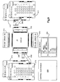
- Figure 1 shows a flat-panel liquid crystal display 10 for use with a document viewer 12 with which the aforementioned method may be employed.
- the particular viewer 12 shown in Figure 1 is a portable electronic viewer for books, news or similar documents, which includes a page selection switch 14 that is integral with the unit and a memory card or floppy disk 16 which can carry the information to be viewed on the document viewer 12.
- a viewer 12 may conveniently include a hard disk drive, a floppy disk drive, and/or various other input/output devices.
- the display 10 is most preferably capable of displaying images as well as text. For displaying images and text it is necessary to refresh or update the display 10 in about one second or less to limit user perception of the updating process. Resolution of the display 10 is quantified in terms of vertical and horizontal lines on the display screen. Present minimum resolution requirements for a page size document viewer is 1,000 lines, which must be capable of being addressed in less than about 1 second.
- the display 10 is constructed using a reflective bistable chiral nematic liquid crystal material whose display state can be controlled by application of a control voltage across the liquid crystal material.
- Suitable chiral nematic liquid crystal materials and cells, as well as their manner of preparation would be known to those of ordinary skill in the art in view of this disclosure.
- Preferred chiral nematic liquid crystal materials and cells are disclosed in, for example, U.S. Patent No. 5,453,863 and U.S. Patent No. 5,437,811, the disclosures of which are incorporated herein by reference.
- a picture element pixel
- Control over each picture element of the display is possible due to the ability of the chiral nematic liquid crystal material to be rapidly updated.
- FIG. 2A The perspective schematic view of Figure 2A shows a small segment of the display 10.
- a layer 50 thickness of 5 microns
- chiral nematic liquid crystal material is sandwiched between two clear containment plates 52, 54 which do not interfere with the light reflecting or transmissive characteristics of the material 50.
- Attached on either side of the plates 52, 54 are arrays of electrodes coupled to a circuit ( Figure 7) described below for energizing the electrodes.
- the plate 52 supports ordered arrays of interconnected electrodes.
- the electrodes on the plate 52 are interconnected to define columns of interconnected electrodes all maintained at the same electrical potential.
- the electrode 60a and all other electrodes that form a column of electrodes are coupled to electrical leads 62 energized at an input 70a along a bottom edge of the display 10.
- the electrode 60b is maintained at the same electrical potential as other interconnected electrodes in its column by the input 70b.
- a third representative electrode 60c is interconnected with other electrodes along the column energized by the input 70c.
- a display state of a picture element directly beneath the electrode 60a is controlled by a voltage difference between the electrode 60a and the voltage on an electrode 80a on the other side of the liquid crystal layer 50 that is supported by the plate 54.
- Three electrodes 80a, 80b, 80c are shown in phantom positioned on an opposite side of the display 10. These electrodes 80a, 80b, 80c are electrically interconnected by electrical leads 82 coupled to an input 90 at the edge of the containment plate 54.
- Selective control of the voltage applied to the electrodes 60a, 80a determine the electric potential applied across the liquid crystal material defining the picture element or pixel beneath the electrodes 60a, 80a.
- this potential can be adjusted and, more specifically, can be controlled in accordance with a method for choosing between a picture element in the focal conic texture and a picture element in the twisted planar texture.
- the drive circuits 58 can present an image or display text on the display.
- Such a display can be updated at rates of at least 500 scan lines per second. It is noted that the electrodes are conceptually represented by circles, e.g. 60a, in Fig. 2A, to facilitate the discussion of the various states of a display shown in Figures 4A - 4F.
- Figure 2B is a second representation more accurately reflecting the structure of a passive matrix type display for application of the inventive method.
- plates 152 and 154 support transparent electrodes 162 and 182a, 182b coated as lines onto the substrates.
- the circles such as 60a in Fig. 2A represent pixels which, as shown at 190a and 190b in Fig. 2B, occur at the intersection of the conductive electrode 162 with conductive electrodes 182a and 182b, respectively.
- FIGS 3A and 3B illustrate a manner in which the display state of a picture element is controlled.
- Chiral nematic liquid crystal material as is known in the art, can be energized by application of a voltage to exhibit multiple optical states or textures.
- Three representative textures for the liquid crystal material are homeotropic, twisted planar, and focal conic.
- the liquid crystal material When in the homeotropic state, the liquid crystal material is transparent to incident light impinging upon the liquid crystal material.
- the focal conic state the liquid crystal material weakly scatters the light, although if the path length is short enough the state can appear transparent, and will appear black when the back substrate is painted black.
- the liquid crystal material reflects the light.
- the final display state of picture elements of liquid crystal material that make up the display 10 is selected in accordance with the inventive method to be in either the focal conic or twisted planar state.
- the liquid crystal in the planar texture reflects light impinging upon the display, and the liquid crystal in the focal conic texture will appear transparent or weakly scattering to provide sufficient contrast with the planar texture. No backlighting is required.
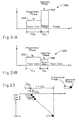
- Figures 3A and 3B display root means square (rms) voltages as a function of time applied across a picture element (pixel) to achieve either the focal conic (3A) or the twisted planar (3B) state.
- each of the control voltages applied to the liquid crystal material starts with a preparation phase 110 of duration T1, during which the liquid crystal material is forced into its homeotropic state.
- the voltage during the preparation phase V P , and the duration of this phase T1 need to be sufficient to cause the complete transformation of the material to the homeotropic texture.
- the preparation stage may be modified to allow less image retention from the initial states of the liquid crystal prior to entering the preparation phase, which degrades the final reflectance from the device.
- the value of V P is higher and the duration of T1 will be longer to avoid this image retention effect.
- the high voltage may be turned on and off several times to place the liquid crystal material completely in the homeotropic state in a shorter time interval T1. In other words, the duration of the preparation phase may be reduced.
- the method After an appropriate time period T1 which, is approximately 40 milliseconds, the method enters the so called selection phase, wherein the liquid crystal material is activated with a selection voltage V S for selecting between the focal conic and twisted planar final state.
- this so-called selection phase 114 lasts only a short period T2 (about one or two milliseconds), much less than the preparation phase 110.
- the selection voltage may be applied to one line at a time, progressing down the rows in pipe-line fashion.
- V S-R the values of V S-R equal to 14 volts and V S-FC equal to 11 volts, this would indicate that about 18 lines could be selected at one time for the material and cell used to produce Fig. 3C.
- the liquid crystal material is energized for a period T3 at an evolution voltage V E less than the preparation voltage, but greater than the selection voltage.
- the liquid crystal material is either maintained in a homeotropic configuration or evolves into a focal conic state.
- the evolution voltage V E of Figures 3A and 3B is removed, the liquid crystal material enters a focal conic ( Figure 3A) or twisted planar ( Figure 3B) final state depending upon the voltage chosen during the selection phase 114.
- V S either has a relatively low voltage V S-FC 120 ( Figure 3A) or a higher voltage V S-R 122 which determines the final state of the picture element to be focal conic or light reflecting twisted planar, respectively.
- FIG. 3C shows the effect of the choice of V E on a graph of selection voltage versus final device reflectance. It can be seen that for V E greater than 34 volts a selection voltage V S of less than 11 volts does not result in a state of lower reflection, and that for V E less than 25 volts the same problem occurs, and the reflection resulting from V S greater than 14 volts is reduced from its maximum value. Thus, with this device it has been found that for proper operation of the addressing scheme V E must be between 25 and 34 volts, with 31 being a preferred value.
- the waveforms depicted in Figures 3A and 3B are root means square voltage representations.
- the actual waveforms are shown in Figures 5 and 6.
- the waveforms are bipolar signals which oscillate above and below ground voltage to avoid ionic conduction to the liquid crystal material sandwiched between the two plates 52, 54.
- the RMS voltages across the liquid crystal material are about 50 volts during the preparation phase 110, 31 volts during the evolution phase 116, and a choice of either 11 volts or 27 volts during the selection phase 114 depending upon the desired final state.
- the column voltage is applied to the display through the whole addressing time period until the end of the evolution stage of the very last row.
- the column voltage V col In order to obtain twisted planar states with high reflectivity, the column voltage V col must be lower than a certain value. If the column voltage is too high, the transition from the homeotropic state to the twisted planar state can not occur and/or the pixels that are already written to the twisted planar state may he switched to the focal conic state.
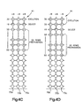
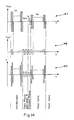
- Figures 4A-4F illustrate a manner in which these voltages are applied by the Figure 7 drive circuit at edge inputs to the electrodes shown in Figure 2.
- Figure 4A this figure depicts a plan view of the electrodes with the intervening structure of the containment plates 52, 54 and liquid crystal material removed for ease in depiction.
- the electrode 60a in the upper left-hand corner of Figure 4A overlies the electrode 80a and, in a similar manner, the two electrodes 60b, 60c overlie the electrodes 80b, 80c.
- Each of 20 rows R1-R20 simultaneously receives a 50 volt RMS signal during the preparation phase 110.
- a first row R1 bounded by three representative column electrodes 60a, 60b, 60c is about to complete its preparation phase 110 and a row R20 is just beginning its preparation phase.
- Voltages applied to the column electrodes of -8 volts, + 8 volts, and the + 8 volts at edge inputs 70a, 70b, 70c are not large enough to disrupt preparation picture elements that make up these 20 rows so that all the pixels of these rows are being converted to the homeotropic state.
- the drive circuits shift the 50-volt RMS signal one row downward as seen in Figure 4B so that 19 of the 20 rows depicted in Figure 4A remain in the preparation phase 110.
- the row R1 of electrodes that includes pairs of electrodes 60a,80a, 60b,80b, 80a,80c on opposite sides of the layer is now energized with bi-polar voltages appropriate for the selection phase 114.
- a 19-volt RMS signal is applied to the edge input 90.
- Drive circuits coupled to the edge inputs 70a, 70b, 70c continue to apply 8-volt RMS signals of controlled polarity to select the state of the pixel element bound by the electrodes in this row R1.
- the picture element bounded by the electrodes 60a,80a has just entered the selection phase. Application of a voltage of -8 volts maintains this picture element in the homeotropic state. As seen in Figure 3B, this will produce a twisted planar configuration for the final state.
- the picture element bounded by the electrodes 60b,80b is energized to cause the pixel between these electrodes to switch to the transient twisted planar state. As seen in Figure 3A, this will result in a focal conic configuration for the picture element in the final state.
- the picture elements bounded by the electrodes depicted in Figures 4A and 4B are labeled with the designation "H" for homeotropic, "P" for twisted planar or "P*" for transient planar to indicate the instantaneous state of the liquid crystal beneath the electrodes.
- the picture element bounded by the two electrodes 60b, 80b has been designated with a "P*" designation in Figure 4B.
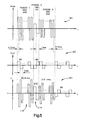
- Waveforms for choosing between either the focal conic or twisted planar end states are shown in Figures 5 and 6.
- square wave RMS signals are applied by the drive circuits to couple an appropriate voltage across a picture element during the selection phase time period T2.
- Three different waveforms are depicted.
- One waveform W1 indicates the row input signals along the input 90, for example.
- a second waveform W2 indicates a column input such as a signal at one of the inputs 70a, 70b, 70c.
- a third waveform W3 indicates the net or resultant signal across the picture element.
- FIG. 5 shows voltage-activation waveforms W4, W5, W6 that allow the liquid crystal material to change from the homeotropic state during the preparation phase 110 to a transient twisted planar state during the selection phase 114. This causes the liquid crystal to switch to a focal conic state after the evolution phase.
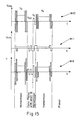
- Figures 4C-4F show continued application of control voltages to the electrode array bounding the liquid crystal layer 50.
- the electrodes in row R 1 bound liquid crystal material entering the evolution phase (see Figures 3A, 3B).
- the electrodes 60b, 80b bounded a picture element where the control voltage at the input 70b allowed a transition to the twisted planar state.
- this picture element enters the focal conic state and ultimately will achieve a focal conic configuration, designated by an "F,” after the evolution stage has ended.
- the picture element bounded by the electrodes 60a, 80a remain in the homeotropic state since, during the selection phase of Figure 4B for row R1, a column control voltage was applied to maintain that picture element in the homeotropic state.
- Figure 4E depicts the row R1 after pixels of that row have experienced the evolution phase.
- the control voltage at the input 90 is reduced to 0 volts.
- the column inputs 70a, 70b, 70c are still selectively switched to activate a row R22 having just completed the preparation phase. This row R22 is spaced from the first row R 1 by 20 other rows.
- Figure 4F shows a situation wherein two rows R1, R2 have reached the end state as indicated by application of 0 volts along the row inputs to these two rows R1, R2.
- the column inputs 70a, 70b, 70c continue to vary depending upon the desired pixel states of a row R23 just beneath the row R22.
- the preparation stage may be modified to allow less image retention from the initial states of the liquid crystal prior to entering the preparation phase, which degrades the final reflectance from the device.
- the preparation stage can include a pre-aligning sequence -- turning the high voltage on and off a few times -- adapted to more completely align the liquid crystal into the homeotropic texture prior to the selection phase.
- the evolution voltage V E is selected to be relatively low, for example 10 to 15 volts, to alter the final state or appearance of the cell.
- the evolution stage may employ voltages to cause evolution of transient planar texture obtained by the selection voltage to reflective planar rather than focal conic.
- the final states that result from the selection phase will be different than those resulting when the evolution voltage is higher in value.
- An advantage of this comparative example is that the states that are present at the end of the evolution time interval are the final states, and no transitions occur at the conclusion of the evolution phase.
- this comparative example differs from the previous comparative example only in the voltage applied following the selection phase and hence, in the resulting liquid crystal states.
- the voltage level in this evolution phase must be chosen to be high enough so that the homeotropic state does not transform into the transient planar state, but low enough so that the transient planar state does not evolve into the focal conic texture and so that the homeotropic state transforms into the focal conic texture.
- the voltage applied to the pixels can be reduced to zero, and because of the zero field bistability of these materials, the pixels that have evolved to the planar texture will remain in that state and pixels that have evolved to the focal conic texture will remain in that state at zero field.
- the method according to this embodiment employs the same preparation and selection phases as described previously. However, in the hold phase, the voltage can be lowered to a lower value or removed entirely and the pixels will remain in the planar or focal conic states obtained during the evolution phase.
- the addressing sequence consists of four phases: preparation, post-preparation, selection and evolution.
- the time interval for the selection phase was about 1 millisecond.
- the time interval for the selection phase and the added post-preparation phase is about 0.5 milliseconds.
- Figures 11A and 11B present the display states of a picture element in a manner similar to that of Figures 3A and 3B.
- Figures 11A and 11B display root means square (rms) voltages as a function of time across a pixel to achieve either a focal conic (11A) or a twisted planar state (11B).
- a control voltage is applied to the liquid crystal material during a preparation phase 300 of duration T1 which forces the liquid crystal material into the homeotropic state.
- duration T1 must be sufficient to cause the complete transformation of the material to the homeotropic texture.
- the values selected for voltage V p and duration T1 are selected based upon the design considerations discussed in the previous embodiment.
- a voltage V i which is a much lower voltage value than the preparation voltage V p , is applied to the liquid crystal material to initiate the transition from the homeotropic texture.
- V i a voltage applied to the liquid crystal material to initiate the transition from the homeotropic texture.
- the polar angle ⁇ of the liquid crystal material changes from 0° to 90°.
- the transition time is about 0.5 ms.
- this transition e changes relatively slowly at the beginning of the transition. This slow interval is defined as t 1 .
- the transition ⁇ then changes very quickly and this faster interval is defined as t 2 .
- t 1 + t 2 is equal to about 0.5 ms, where t 1 is the post-preparation phase 312 with a duration of about 0.2 ms and t 2 is the selection phase.
- the selection period (T2) covers the interval t 1 + t 2 .
- the applied voltage V i is relatively low and the material is allowed to relax through a conic helical structure to the transient planar state.
- the polar angle ⁇ only slightly deviates from 0°.
- a voltage V s is applied to the liquid crystal material for selecting between the focal conic and twisted planar final state.
- Voltage V s may be a high voltage V r 316 which stops the growth of the polar angle ⁇ and switches the material back into the homeotropic state.
- the value for voltage V r is much greater than the value for V i .
- the voltage V s may be a low voltage V b 318 which lets the polar angle ⁇ continue to grow to 90° which causes the material to relax further to the transient planar state.
- the value for voltage V b is only slightly greater than the value for V i . As seen in Fig.
- the time interval t 2 for the polar angle ⁇ to change from ⁇ ⁇ 5° to 90° is about 0.2 ms for a cholesteric liquid crystal material reflecting visible light.
- the voltage to switch the material back to the homeotropic texture depends on the polar angle of the material.
- a cholesteric material with a large polar angle requires a high voltage to force the material to the homeotropic texture.
- a voltage V e is applied to the liquid crystal material to force the material into either the focal conic texture if the material is selected to the transient planar texture in the selection phase or is kept in the homeotropic texture if the material is selected to be in the homeotropic texture in the selection phase.
- the value for voltage V e is less than the preparation voltage, but greater than the post-preparation voltage.
- various factors such as contrast ratio and drive speed need to be considered when selecting a value for the selection voltage V e and the duration time T3.
- the applied voltage is smaller than V' pf which is the voltage for the planar-focal conic transition. If the liquid crystal material is in the homeotropic texture then it relaxes into the reflecting planar state. If the material is switched into the focal conic state, then the material remains in the substantially transparent focal conic state.
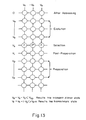
- Figure 13 presents a sequence in which voltages are applied to the electrodes shown in Figure 2.
- Figure 13 presents the addressing method applied to the respective row and column electrodes.
- Voltages V o and -V o are applied to the column electrodes while the preparation, post-preparation, selection and evolution voltages are sequentially applied to the row electrodes.
- the pixels bounded by electrodes depicted in Figure 13 are labeled with the designation "F" or "P*" to indicate the states of the liquid crystal material between the electrodes during addressing.
- waveform W7 shows the row input voltage
- waveform W8 shows the column input voltage
- waveform W9 shows the resultant or combined signal of W7 and W8 across the picture element.
- the waveforms shown in Figure 14 allow the liquid crystal material to change from the homeotropic state during the preparation phase 300 to a transient planar state during the selection phase 314. This causes the liquid crystal material to switch to a focal conic state after the evolution phase 320.
- waveform W10 shows the row input voltage
- waveform W11 shows the column input voltage
- waveform W12 shows the resultant or combined signal of W10 and W11 across the picture element.
- Waveforms W10 - W12 maintain the liquid crystal material in a homeotropic state during the selection phase which results in a twisted planar final state for the pixel.
- a voltage sequence applied to a liquid crystal cell as described above This example is in no way limiting and is exemplary of the improved transition time.
- a green reflecting sample with PMMA coating was constructed and had the following sequence of voltage signals applied thereto.
- Preparation phase 40 ms, 60 V
- Post-preparation phase 0.2 ms, 6 V
- Selection phase 0.2 ms Evolution phase: 40 ms, 29 V
- the final reflection vs. selection voltage graphical representation is shown in Figure 16.
- a high reflection value is obtained with a selection voltage higher than 27 V.
- a low reflection value is obtained with a selection voltage lower than 15 V.
- gray scales can be obtained with selection voltages in the range of 15 V to 27 V.
- gray scale can also be obtained by using time-modulation techniques.
- V i the same voltage as the post-preparation voltage V i is applied and then a higher voltage V s is applied for ⁇ t.
- V s 35 V is applied to the above example, the final reflection vs. ⁇ t showing the different gray scale values is shown in Figure 18.
- an after-selection phase 330 is inserted between the selection phase 318 and the evolution phase 320.
- the overall addressing time for the flat panel display can be reduced to about 22 ms.
- Figures 19A and 19B present the display states of a picture element correlated to a root means square (rms) voltage as a function of time across the appropriate electrodes.
- the preparation phase 300 applies a voltage V p sufficiently high during ⁇ t p to drive the liquid crystal material to a homeotropic texture which causes the polar angle.of the director of the liquid crystal material to rotate to a zero degree position.
- This applied voltage is primarily provided by a row driver that powers the row electrodes.
- the applied voltage V pp is sufficiently low or reduced during ⁇ t pp to allow the liquid crystal material to relax.
- the polar angle of the liquid crystal director exhibits a slight increase in value.
- a voltage V s is applied during ⁇ t s which ultimately determines the final appearance of the liquid crystal material.
- a high voltage 316 stops the relaxation of the liquid crystal material to a transient planar texture and returns the material back to the homeotropic texture.
- a low voltage 318 allows the liquid crystal material to continue relaxation to the transient planar texture and the director's polar angle becomes relatively large.
- Application of the voltage V s is achieved by combining the voltages generated by the row drivers and a column driver that powers the column electrodes.
- an after-selection phase 330 a voltage V as is applied during ⁇ t as and is relatively low.
- the liquid crystal material behaves as follows. If a homeotropic texture is selected in the selection phase 314, then the after-selection phase 330 causes the liquid crystal material to relax toward the transient planar texture slightly. In other words, the polar angle returns to a small non-zero value. However, if the transient planar texture is selected in the selection phase 314, then the after-selection phase 330 almost completely transforms the liquid crystal material to the transient planar texture wherein the director's polar angle is almost 90°.
- the column driver supplies the voltage V as .
- a relatively intermediate voltage V e is applied in the evolution phase 320 .
- the liquid crystal material deviates slightly from the homeotropic texture in the after-selection phase 330, then the material is switched back to the homeotropic texture or held in a state slightly deviated from the homeotropic texture.
- the voltage when the voltage is sufficiently low, the material relaxes to the transient planar texture and then to the stable planar texture.
- the liquid crystal material switches to the focal conic texture in evolution phase 320. Accordingly, the liquid crystal material remains in the focal conic texture and the material appears transparent or weakly scattering.
- the voltage supplied in the evolution phase is supplied mostly from the row driver.
- V preparation post-preparation selection after-selection evolution voltage
- V preparation post-preparation selection after-selection evolution voltage
- ms pulse width
- Hz frequency
- a 5 ⁇ m cell was made with a cholesteric liquid crystal material having a pitch length that reflects yellow light.
- the voltage V s in the selection phase 314 is at or below 32 volts, the focal conic texture is obtained after the evolution phase 320.
- the voltage V s in the selection phase 314 is at or above 48 volts, the planar texture is obtained.
- the duration ⁇ t s is about 0.05 ms.
- these and the other values listed in table may vary according to the liquid crystal material and other factors. It will be appreciated that the voltages applied in this example may either be in the form of square waves or sine waves.
- the column and row voltages for the five phase drive scheme are represented in Fig. 20.
- the values of the row voltages vary during the five phases according to the desired texture.
- the row voltage is 29V and is applied at a frequency of 1 kHz. Therefore the rms voltage across the pixels is about 30V.
- the row voltage is 0V, and the voltage across the pixels after the addressing sequence is 8V with no cross-talking effect.
- the five phase drive scheme provides an improvement over other drive schemes by pre-disposing the polar angle of the liquid crystal directors.
- the selection interval is shorter than in the four phase drive scheme. This reduces the overall frame time to address the picture.
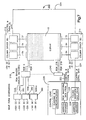
- Figure 7 is a block diagram of a circuit 200 for energizing edge contacts to achieve a specified output from the display 10.
- the particular display depicted in Figure 7 is a matrix of 320 by 320 picture elements. This display thus includes 320 rows with each row having 320 individually controllable picture elements.
- each row and each column of the display 10 has an contact or connector at the edge of the display for coupling a control voltage to an electrode that extends across the display.
- the block diagram of Figure 7 shows the circuits for energizing or driving these edge contacts divided into groups spaced about the outer periphery of the display.
- a group of row drivers 210 on one side of the display activates edge contacts coupled to the even rows (0,2,4 etc) in the display and a second group of row drivers 212 on the opposite side of the display activates edge contacts coupled to the odd rows (1, 3, 5 etc) of the display.
- a group of column drivers 214 activates the even columns and a second group of column drivers 216 activates the odd columns.
- Each of the sets of row and column drivers is electrically connected to a control/logic circuit 220 which controls the presentation of data on the display 10.
- Data and control signals from the control/logic circuit 220 are presented on two control data busses 222, 224. Data on these two busses is output from two electronically programmable memory circuits 22b, 228. Control signals are generated from a logic portion of the circuit 220.
- the row drivers 210 on the left of the display in Figure 7 is made up of 160 analog switches 240 connected in series. A functional block diagram of one of these switches is depicted in Figure 10.
- a preferred analog switch used to construct the row drivers is model HV204 analog switch commercially available from Supertex.
- each analog switch 240 includes a data input 242, a data output 244 and an eight bit shift register 246 for holding data.
- the data consists of two state data bits.
- Data at the data input 242 is clocked into the shift register 246 by toggling a clock input 248.
- the shift register has eight parallel outputs 246a - 246h. Data at these outputs is presented to eight latch circuits 250a - 250h. Each of these latch circuits has a clear input CL and a latch enable input NOT LE connected to the control portion of the control/data bus 222. The latch is cleared upon application of a signal to the clear input and latches the data presented at a D input to the latch upon receipt of a load enable signal. The data latched into the latch is presented at an output from the latch and communicated through an associated one of eight level shifters 252a - 252h.
- Each of the analog switches 240 also includes eight switch or output portions 254a - 254h.
- the status of the latch determines the state of an associated output or switch portion of the analog switch. If the latch contains a high bit the switch output closes and if the latch has a low bit the switch output opens. As a specific example, if the latch 250h has a high bit latched from the shift register, the switch portion 254h connects together two contacts 260, 262 seen in Figure 10.
- each of the analog switches 240 has two input pins that are connected to a + /- 50 volt waveform, two pins connected to a +/- 30 volt waveform, two pins connected to a +/-19 volt waveform and two pins that are grounded. Outputs associated with these four different voltage inputs are coupled together. This is seen in Figure 10 where one sees that the switch portion 254a is connected to a +/- 50 volt signal, the switch portion 254b is connected to a +/- 30 volt signal, the switch portion 254c is connected to the +/- 19 volt signal and the input to the switch portion 254d is grounded. Also note that the outputs from each of these switch portions are connected together and also connected to row 0 of the display 10.
- a series of bits appropriate to achieve twenty preparation cycles, one selection cycle, and then twenty evolution cycles are shifted into a bottommost analog switch 240 and shifted up through all the row drivers by appropriate clocking of the clock inputs to the shift registers.
- the control 220 After each clock signal the control 220 causes the latches to simultaneously latch data for appropriate energization of edge contacts.
- the control 220 co-ordinates the presentation and clocking of data so that the row drivers receives the appropriate data.
- each row of the 320 rows in the display is energized with a bi-polar selection signal.
- the state of each pixel (twisted planar or focal conic) in that row is stored in a second electronically controllable memory 228.
- Each time the row driver configuration changes it is the responsibility of the control circuit 220 to load the correct column data into the two column drivers 214, 216.
- the purpose of the column drivers 214, 216 is to control the phase of the +/- 8 volt signal for each of the 320 pixels of the row that is experiencing the selection phase.
- the preferred column drivers 214, 216 are built using SMOS column driver integrated circuits (identified by part number SED1191f). Each of the two column drivers is built on a circuit board 220 that has +8 volt and -8 volt inputs 270, 272 that drive the column edge contacts such as the representative contacts 70a, 70b, 70c of the display 10.
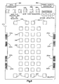
- FIG. 8 A layout of a row driver printed circuit board 274 supporting forty of the analog switches 240 is shown in Figure 8. Since the row drivers 210 require 160 such analog switches, the drivers 210 are made up from four circuit boards 274, 275, 276, 277 ( Figure 9).
- the circuit board depiction in Figure 8 includes three analog switches 280, 282, 284 that are waveform generators for providing bi-polar signals to the other forty analog switches on the circuit board 274.
- the analog switch 280 provides a square wave bi-polar (+/-) 50 volt signal that is connected to each of the analog switches 240.
- the analog switch 282 provides a bi-polar (+/-) 30 volt signal and the analog switch 284 provides a bi-polar (+/-) 19 volt signal.
- the square wave output from the waveform generators is achieved by coupling one positive and one negative voltage of the appropriate magnitude to two analog switch inputs and connecting together the outputs associated with those inputs.
- the bi-polar output from the switch is provided.
- the circuit board 274 includes a number of input and output connectors for interfacing.
- One connector 290 connects to the control and data bus 222 to supply control and data signals to the board.
- a power supply connector 292 provides the appropriate power signals to the board from a regulated power supply 300 shown in Figure 9.
- Edge connectors 294a - 294h on opposite sides of the board output row drive signals to a transition printed circuit board 296 ( Figure 9) that multiplexes the row drive signals to an appropriate row electrode of the display 10.
- the connector 294a supplies twenty signals for driving twenty rows of the display. These twenty signals are coupled to a flexible multi-conductor printed circuit cable 298 having contacts at one end to engage one of the connectors 294a -294h. An opposite end of the cable 298 has contacts that engage a connector on the transition printed circuit board 296.
- the circuity for the column drivers is mounted to the two printed circuit boards 214, 216. These circuit boards not only support the circuitry for applying an appropriate phase signal to the pixels across a row in the display undergoing the selection phase, but also includes the circuitry for routing the signals from the circuits to the edge contacts of the display 10.
- the column driver boards 214, 216 each include three SMOS 1191f display driver integrated circuits and necessary capacitors, resistors, level translators and an analog switch that serves as a ground switch.
- Each of the SMOS circuits has its own data input from the 8 bit parallel data bus 224.
- Each clock pulse of the column board driver boards gathers a byte of data so that each of the six driver integrated circuits gets one data bit on each clock signal. Since of the integrated circuits has 64 outputs, it requires 64 data bytes on the bus 224 to completely configure a row. Thus as the selection phase reaching each new row, 64 bytes of column data is loaded into the driver boards 214, 216 to control the appropriate phase of the +/- 8 volt square wave signal output from the boards 214, 216.
Claims (16)
- Ein Verfahren zum Adressieren eines bistabilen, chiral-nematischen Flüssigkristallmaterials (50), welches zwischen Elektroden (60a, 60b, 60c, 80a, 80b, 80c) angeordnet ist, die auf gegenüberliegenden Seiten des Flüssigkristalls angeordnet sind und eingerichtet sind, um selektiv ein elektrisches Feld durch das Flüssigkristallmaterial hindurch anzulegen, wobei das Verfahren die Schritte umfasst:Ansteuern der Elektroden (60a, 60b, 60c, 80a, 80b, 80c), um während einer Vorbereitungsphase (300) eine Vorbereitungsspannung über dem Flüssigkristall aufzubauen, wobei die Vorbereitungsphase den Flüssigkristall dazu veranlasst, sich in einem im Wesentlichen homöotropischen Zustand auszurichten;Ansteuern der Elektroden, um während einer Postvorbereitungsphase (312) eine Postvorbereitungsspannung über dem Flüssigkristall aufzubauen, wobei die Postvorbereitungsphase den Flüssigkristall dazu veranlasst, einen Übergang vom homöotropischen Zustand in einen transienten planaren Zustand zu initiieren;Ansteuern der Elektroden, um während einer Auswahlphase (314) zum Auswählen eines endgültigen Anzeigezustands für den Flüssigkristall eine Auswahlspannung über dem Flüssigkristall aufzubauen, wobei die Auswahlspannung das Flüssigkristallmaterial entweder in der homöotropischen oder der transienten planaren Struktur platziert;Ansteuern der Elektroden, um während einer Entwicklungsphase (320) eine Entwicklungsspannung über dem Flüssigkristall aufzubauen, und wobei dem Flüssigkristall danach erlaubt wird, den endgültigen Anzeigezustand aufzuweisen, wobei, während der Entwicklungsphase, sich der Flüssigkristall im transienten planaren Strukturzustand nach der Auswahlphase in einen fokal-konischen Zustand entwickelt und der Flüssigkristall im homöotropischen Zustand nach der Auswahlphase im homöotropischen Zustand verbleibt; undAnsteuern der Elektroden, um während einer Haltephase unmittelbar nach der Entwicklungsphase eine Haltespannung, welche kleiner ist als die Spannung für einen Übergang von planar zu fokal-konisch, über dem Flüssigkristall aufzubauen, so dass Pixel im fokal-konischen Zustand nach der Entwicklungsphase in diesem Zustand verbleiben, während Pixel im homöotropischen Zustand in den reflektierenden verdrehten planaren Zustand relaxieren, dadurch gekennzeichnet, dass:das Verfahren ein Ansteuern der Elektroden umfasst, um während einer Nachauswahlphase (330) unmittelbar nach der Auswahlphase eine Nachauswahlspannung über dem Flüssigkristall aufzubauen, um den Polarwinkel des Flüssigkristallmaterials dort anzupassen, wo die Nachauswahlspannung geringer als die Entwicklungsspannung, ähnlich der Postvorbereitungsspannung und verschieden von der Auswahlspannung ist.
- Das Verfahren nach Anspruch 1, wobei nach der Entwicklungsphase (320) die Entwicklungsspannung an den Elektroden reduziert wird, um dem Flüssigkristall zu erlauben, einen seiner endgültigen Anzeigezustände aufzuweisen.
- Das Verfahren nach Anspruch 1, wobei die Vorbereitungsspannung einen Wert besitzt und die Vorbereitungsphase (300) von einer Dauer ist, um das Kristallmaterial homöotropisch auszurichten.
- Das Verfahren nach Anspruch 1, wobei der Wert der Auswahlspannung ausgewählt wird, um den Flüssigkristall entweder in einer homöotropischen Struktur beizubehalten oder um dem Flüssigkristall zu erlauben, einen Übergang zu einer transienten verdrehten planaren Struktur zu initiieren.
- Das Verfahren nach Anspruch 1, wobei der Flüssigkristall ein chiral-nematischer Flüssigkristall ist und die Auswahlspannung einen Wert besitzt der ausreicht, um entweder einen fokal-konischen oder einen verdrehten planaren endgültigen Anzeigezustand aufzubauen.
- Das Verfahren nach Anspruch 1, wobei die Entwicklungsspannung einen Wert besitzt und die Entwicklungsphase (320) von einer Dauer ist, um einen Flüssigkristall, der in einer homöotropischen Struktur ist, in der homöotropischen Struktur beizubehalten, und um einen Flüssigkristall in einer transienten verdrehten planaren Struktur zu erlauben, sich während der Entwicklungsphase in eine fokal-konische Struktur zu entwickeln.
- Das Verfahren nach Anspruch 1, wobei die Entwicklungsspannung einen Wert besitzt und die Entwicklungsphase (320) von einer Dauer ist die wirksam sind, um einem Flüssigkristall in einer transienten verdrehten planaren Struktur zu erlauben, in eine fokal-konische Struktur zu relaxieren, und um einem Flüssigkristall in einer homöotropischen Struktur zu erlauben, während der Entwicklungsphase (370) in der homöotropischen Struktur zu verbleiben und danach in einer reflektierenden verdrehten planaren Struktur.
- Das Verfahren nach Anspruch 1, wobei die Vorbereitungsphase (300) eine Ein-/Aus-Modulation der Vorbereitungsspannung umfasst, um die Dauer der Vorbereitungsphase zu verkürzen.
- Das Verfahren nach Anspruch 1, wobei der chiralnematische Flüssigkristall eine Neigungslänge in der verdrehten planaren Struktur besitzt die wirksam ist, um Licht im sichtbaren Spektrum zu reflektieren.
- Das Verfahren nach Anspruch 1, wobei der Schritt des Ansteuerns der Elektroden (60a, 60b, 60c, 80a, 80b, 80c) den Schritt der Zeitmodulation der Elektroden während der Auswahlphase (314) umfasst, um das Flüssigkristallmaterial zu veranlassen, Graustufungseigenschaften aufzuweisen.
- Das Verfahren nach Anspruch 1, wobei der Schritt des Ansteuerns der Elektroden (60a, 60b, 60c, 80a, 80b, 80c) den Schritt der Amplitudenmodulation der Elektroden während der Auswahlphase (314) umfasst, um das Flüssigkristallmaterial zu veranlassen, Graustufeneigenschaften aufzuweisen.
- Eine Anzeigevorrichtung, umfassend:a) eine Schicht aus bistabilem, chiral-nematischem Flüssigkristallmaterial (50);b) mehrere Elektroden (60a, 60b, 60c, 80a, 80b, 80c), die auf gegenüberliegenden Seiten der Flüssigkristallschicht (50) beabstandet sind zum Anlegen ausgewählter Aktivierungsspannungen über mehreren Bildelementen der Flüssigkristallschicht; undc) Steuerelektronik (200) zum sequentiellen Einstellen eines Anzeigezustands mehrerer Bildelemente der Flüssigkristallschicht, umfassend Schaltungen die eingerichtet sind, um:dadurch gekennzeichnet, dass die Schaltung eingerichtet ist, um während einer Nachauswahlphase (330) unmittelbar nach der Auswahlphase (314) eine Nachauswahlspannung über dem ausgewählten Bildelement anzulegen, um den Polarwinkel des Flüssigkristalls anzupassen, wobei die Nachauswahlspannung geringer als die Entwicklungsspannung, ähnlich der Postvorbereitungsspannung und verschieden von der Auswahlspannung ist, um ein Erreichen des Anzeigezustands zu beschleunigen, und wobei die Steuerelektronik des Weiteren Schaltungen (220) zum Anlegen der Nachauswahlspannung an den mehreren Bildelementen und einen Timer umfasst, um die Dauer der Nachauswahlspannung zu steuern.i) während einer Vorbereitungsphase (300) eine Vorbereitungsspannung über einem ausgewählten Bildelement anzulegen, wobei die Vorbereitungsphase (300) den Flüssigkristall dazu veranlasst, sich in einem homöotropischen Zustand auszurichten;ii) während einer Postvorbereitungsphase (312) eine Postvorbereitungsspannung über dem ausgewählten Bildelement anzulegen, wobei die Postvorbereitungsphase (312) den Flüssigkristall dazu veranlasst, einen Übergang vom homöotropischen Zustand in einen transienten planaren Zustand zu initiieren;iii) während einer Auswahlphase (314) eine Auswahlspannung über dem ausgewählten Bildelement anzulegen, um einen vorbestimmten endgültigen Anzeigezustand auszuwählen, wobei die Auswahlspannung, die an dem Bildelement angelegt wird, die Flüssigkristallschicht entweder in der homöotropischen oder transienten planaren Struktur platziert und so gewählt ist, dass ein endgültiger optischer Zustand des Bildelements ein fokal-konischer Zustand oder ein verdrehter planarer Zustand ist; undiv) während einer Entwicklungsphase (320) eine Entwicklungsspannung über dem ausgewählten Bildelement anzulegen, wobei, während der Entwicklungsphase (320), sich der Flüssigkristall in der transienten planaren Struktur nach der Auswahlphase in einen fokal-konischen Zustand entwickelt und der Flüssigkristall im homöotropischen Zustand nach der Auswahlphase im homöotropischen Zustand verbleibt; undv) eine Haltespannung, welche kleiner ist als die Spannung für einen Übergang von planar zu fokal-konisch, über dem Flüssigkristall während einer Haltephase unmittelbar nach der Entwicklungsphase anzulegen, so dass Pixel im fokal-konischen Zustand nach der Entwicklungsphase in diesem Zustand verbleiben, während Pixel im homöotropischen Zustand in den reflektierenden verdrehten planaren Zustand relaxieren;
- Die Vorrichtung nach Anspruch 12, wobei Elektroden (162) auf einer Seite der Flüssigkristallschicht in generell parallelen Reihen angeordnet sind und Elektroden (182a, 182b) auf einer gegenüberliegenden Seite der Flüssigkristallschicht in generell parallelen Spalten angeordnet sind, die im Wesentlichen orthogonal zu den Reihen sind, und die Bildelemente sind durch die Punkte (190a, 190b) an den Reihen und Spalten definiert, an denen sich die Reihen und Spalten schneiden würden, wenn sie in der gleichen Ebene sind, wobei, wenn die Steuerelektronik ein Spannungssignal an einer Reihenelektrode anlegt, alle Bildelemente in dieser Reihe elektrisch an das gleiche Spannungssignal angeschlossen sind, und wenn die Steuerelektronik (220) ein Spannungssignal an einer Spaltenelektrode anlegt, alle Bildelemente in dieser Spalte an das gleiche Spannungssignal angeschlossen sind.
- Die Vorrichtung nach Anspruch 12, wobei die Steuerelektronikschaltungen (220) die Schicht aus bistabilem, chiral-nematischem Flüssigkristallmaterial während der Auswahlphase a priori in einem anderen Zustand als den vorbestimmten endgültigen Anzeigezustand anordnen.
- Die Vorrichtung nach Anspruch 12, wobei die Steuerelektronik (220) ein Anlegen des Auswahlsignals so zeitmoduliert, dass der vorbestimmte endgültige Anzeigezustand Graustufungseigenschaften aufweist.
- Die Vorrichtung nach Anspruch 12, wobei die Steuerelektronik (220) ein Anlegen des Auswahlsignals so amplitudenmoduliert, dass der vorbestimmte endgültige Anzeigezustand Graustufeneigenschaften aufweist.
Applications Claiming Priority (3)
| Application Number | Priority Date | Filing Date | Title |
|---|---|---|---|
| US852319 | 1992-03-18 | ||
| US08/852,319 US6154190A (en) | 1995-02-17 | 1997-05-07 | Dynamic drive methods and apparatus for a bistable liquid crystal display |
| PCT/US1998/009259 WO1998050804A2 (en) | 1997-05-07 | 1998-05-06 | Dynamic drive methods and apparatus for a bistable liquid crystal display |
Publications (3)
| Publication Number | Publication Date |
|---|---|
| EP0954841A4 EP0954841A4 (de) | 1999-11-10 |
| EP0954841A2 EP0954841A2 (de) | 1999-11-10 |
| EP0954841B1 true EP0954841B1 (de) | 2006-05-17 |
Family
ID=25313022
Family Applications (1)
| Application Number | Title | Priority Date | Filing Date |
|---|---|---|---|
| EP98920306A Expired - Lifetime EP0954841B1 (de) | 1997-05-07 | 1998-05-06 | Dynamische antriebsverfahren und gerät für eine bistabile flüssigkristallanzeige |
Country Status (10)
| Country | Link |
|---|---|
| US (1) | US6154190A (de) |
| EP (1) | EP0954841B1 (de) |
| JP (1) | JP3961578B2 (de) |
| KR (1) | KR20000022562A (de) |
| CN (1) | CN1188821C (de) |
| AT (1) | ATE326752T1 (de) |
| AU (1) | AU7291198A (de) |
| DE (1) | DE69834547T2 (de) |
| IL (1) | IL127866A0 (de) |
| WO (1) | WO1998050804A2 (de) |
Families Citing this family (150)
| Publication number | Priority date | Publication date | Assignee | Title |
|---|---|---|---|---|
| US5877738A (en) * | 1992-03-05 | 1999-03-02 | Seiko Epson Corporation | Liquid crystal element drive method, drive circuit, and display apparatus |
| US7193625B2 (en) | 1999-04-30 | 2007-03-20 | E Ink Corporation | Methods for driving electro-optic displays, and apparatus for use therein |
| US7999787B2 (en) | 1995-07-20 | 2011-08-16 | E Ink Corporation | Methods for driving electrophoretic displays using dielectrophoretic forces |
| DE19731020A1 (de) * | 1997-07-18 | 1999-01-21 | Hoechst Ag | Ferroelektrisches Flüssigkristalldisplay mit breitem Arbeitstemperaturbereich |
| US20010015723A1 (en) * | 1998-05-01 | 2001-08-23 | Hoi-Sing Kwok | Method and apparatus for driving reflective bistable cholesteric displays |
| US20020167500A1 (en) * | 1998-09-11 | 2002-11-14 | Visible Techknowledgy, Llc | Smart electronic label employing electronic ink |
| US6924781B1 (en) | 1998-09-11 | 2005-08-02 | Visible Tech-Knowledgy, Inc. | Smart electronic label employing electronic ink |
| US6888522B1 (en) * | 1999-03-31 | 2005-05-03 | Minolta Co., Ltd. | Information display apparatus |
| US7119772B2 (en) | 1999-04-30 | 2006-10-10 | E Ink Corporation | Methods for driving bistable electro-optic displays, and apparatus for use therein |
| US6531997B1 (en) * | 1999-04-30 | 2003-03-11 | E Ink Corporation | Methods for addressing electrophoretic displays |
| US7012600B2 (en) * | 1999-04-30 | 2006-03-14 | E Ink Corporation | Methods for driving bistable electro-optic displays, and apparatus for use therein |
| US6504524B1 (en) * | 2000-03-08 | 2003-01-07 | E Ink Corporation | Addressing methods for displays having zero time-average field |
| US6518944B1 (en) * | 1999-10-25 | 2003-02-11 | Kent Displays, Inc. | Combined cholesteric liquid crystal display and solar cell assembly device |
| US6812913B2 (en) | 2000-02-17 | 2004-11-02 | Minolta Co., Ltd. | Liquid crystal display driving method and liquid crystal display device |
| JP4710158B2 (ja) * | 2000-04-03 | 2011-06-29 | 旭硝子株式会社 | メモリ性コレステリック液晶表示装置の駆動方法および駆動装置 |
| US6950086B2 (en) * | 2000-04-03 | 2005-09-27 | Optrex Corporation | Driving method for a cholesteric liquid crystal display device having a memory mode of operation and a driving apparatus |
| WO2001082283A1 (en) | 2000-04-25 | 2001-11-01 | Koninklijke Philips Electronics N.V. | Driving of display device for obtaining gray scales |
| JP4706123B2 (ja) * | 2000-05-29 | 2011-06-22 | コニカミノルタホールディングス株式会社 | 液晶表示装置及び液晶表示素子の駆動方法 |
| JP2002101316A (ja) * | 2000-09-26 | 2002-04-05 | Mitsubishi Electric Corp | クロック生成回路及び画像表示装置 |
| GB0024487D0 (en) * | 2000-10-05 | 2000-11-22 | Koninkl Philips Electronics Nv | Bistable chiral nematic liquid crystal display and method of driving the same |
| US6906705B2 (en) * | 2000-10-16 | 2005-06-14 | Matsushita Electric Industrial Co., Ltd. | Electronic file with flexible display medium |
| US7023409B2 (en) | 2001-02-09 | 2006-04-04 | Kent Displays, Incorporated | Drive schemes for gray scale bistable cholesteric reflective displays utilizing variable frequency pulses |
| JP4258128B2 (ja) * | 2001-03-13 | 2009-04-30 | コニカミノルタホールディングス株式会社 | 液晶表示素子の駆動方法及び液晶表示装置 |
| MXPA03008349A (es) * | 2001-03-16 | 2004-10-15 | Johnson & Johnson | Parche transdermico para administrar fentanilo. |
| US7116287B2 (en) * | 2001-05-09 | 2006-10-03 | Eastman Kodak Company | Drive for cholesteric liquid crystal displays |
| US8342938B2 (en) | 2001-09-27 | 2013-01-01 | Igt | Gaming machine reel having a rotatable dynamic display |
| JP3606830B2 (ja) * | 2001-11-02 | 2005-01-05 | 株式会社ジーニック | コレステリック液晶ディスプレイ用ドライバ |
| US8558783B2 (en) | 2001-11-20 | 2013-10-15 | E Ink Corporation | Electro-optic displays with reduced remnant voltage |
| US7952557B2 (en) | 2001-11-20 | 2011-05-31 | E Ink Corporation | Methods and apparatus for driving electro-optic displays |
| US8125501B2 (en) | 2001-11-20 | 2012-02-28 | E Ink Corporation | Voltage modulated driver circuits for electro-optic displays |
| US8593396B2 (en) | 2001-11-20 | 2013-11-26 | E Ink Corporation | Methods and apparatus for driving electro-optic displays |
| US7528822B2 (en) | 2001-11-20 | 2009-05-05 | E Ink Corporation | Methods for driving electro-optic displays |
| US9530363B2 (en) | 2001-11-20 | 2016-12-27 | E Ink Corporation | Methods and apparatus for driving electro-optic displays |
| US9412314B2 (en) | 2001-11-20 | 2016-08-09 | E Ink Corporation | Methods for driving electro-optic displays |
| JP3928438B2 (ja) | 2001-11-30 | 2007-06-13 | コニカミノルタホールディングス株式会社 | 液晶表示素子の駆動方法、駆動装置及び液晶表示装置 |
| KR100537609B1 (ko) * | 2001-12-27 | 2005-12-19 | 삼성에스디아이 주식회사 | 정확한 계조 표시를 위한 콜레스테릭 액정 표시 패널의구동 방법 |
| KR100592237B1 (ko) * | 2001-12-27 | 2006-06-23 | 삼성에스디아이 주식회사 | 알.엠.에스(r.m.s) 전압을 이용한 콜레스테릭 액정표시 패널의 구동 방법 |
| US20030122752A1 (en) * | 2002-01-03 | 2003-07-03 | Yao-Dong Ma | Localized driving means for cholesterics displays |
| KR100603281B1 (ko) * | 2002-02-15 | 2006-07-20 | 삼성에스디아이 주식회사 | 두 전위들로써 주사 전극 라인들을 구동하여 계조를표시하기 위한 콜레스테릭 액정 표시 패널의 구동 방법 |
| JP3891018B2 (ja) * | 2002-02-18 | 2007-03-07 | コニカミノルタホールディングス株式会社 | 液晶表示素子の駆動方法、駆動装置及び液晶表示装置 |
| FR2838858B1 (fr) * | 2002-04-19 | 2004-08-27 | Nemoptic | Dispositif d'affichage bistable a cristaux liquides comprenant des moyens d'adressage perfectionnes |
| US6894668B2 (en) * | 2002-05-03 | 2005-05-17 | Eastman Kodak Company | General 2 voltage levels driving scheme for cholesterical liquid crystal displays |
| JP2003344821A (ja) * | 2002-05-30 | 2003-12-03 | Nanox Corp | 液晶表示装置 |
| US20080024482A1 (en) | 2002-06-13 | 2008-01-31 | E Ink Corporation | Methods for driving electro-optic displays |
| TW200401915A (en) * | 2002-07-26 | 2004-02-01 | Varintelligent Bvi Ltd | High contrast black-and-white chiral nematic displays |
| US20040046705A1 (en) * | 2002-09-20 | 2004-03-11 | Minolta Co., Ltd. | Liquid crystal display apparatus |
| WO2004029702A1 (ja) * | 2002-09-27 | 2004-04-08 | Nanox Corporation | コレステリック液晶表示装置およびコレステリック液晶表示素子の駆動方法 |
| IL152029A0 (en) | 2002-09-30 | 2003-04-10 | Magink Display Technologies | Distinct color lcd apparatus |
| US20130063333A1 (en) | 2002-10-16 | 2013-03-14 | E Ink Corporation | Electrophoretic displays |
| JP3714324B2 (ja) * | 2002-12-24 | 2005-11-09 | コニカミノルタホールディングス株式会社 | 液晶表示装置 |
| US6885357B2 (en) * | 2002-12-31 | 2005-04-26 | Eastman Kodak Company | Method for writing pixels in a cholesteric liquid crystal display |
| US6924783B2 (en) * | 2003-01-28 | 2005-08-02 | Eastman Kodak Company | Drive scheme for cholesteric liquid crystal displays |
| US6911965B2 (en) * | 2003-01-28 | 2005-06-28 | Kent Displays Incorporated | Waveform sequencing method and apparatus for a bistable cholesteric liquid crystal display |
| FR2851683B1 (fr) * | 2003-02-20 | 2006-04-28 | Nemoptic | Dispositif et procede perfectionnes d'affichage a cristal liquide nematique bistable |
| US10726798B2 (en) | 2003-03-31 | 2020-07-28 | E Ink Corporation | Methods for operating electro-optic displays |
| JP3818273B2 (ja) * | 2003-05-23 | 2006-09-06 | コニカミノルタホールディングス株式会社 | 液晶表示素子の駆動方法及び液晶表示装置 |
| US8174490B2 (en) | 2003-06-30 | 2012-05-08 | E Ink Corporation | Methods for driving electrophoretic displays |
| WO2005081779A2 (en) | 2004-02-19 | 2005-09-09 | Kent Displays Incorporated | Staked display with shared electrode addressing |
| US7236151B2 (en) | 2004-01-28 | 2007-06-26 | Kent Displays Incorporated | Liquid crystal display |
| US7190337B2 (en) * | 2003-07-02 | 2007-03-13 | Kent Displays Incorporated | Multi-configuration display driver |
| JP4806634B2 (ja) | 2003-08-19 | 2011-11-02 | イー インク コーポレイション | 電気光学ディスプレイおよび電気光学ディスプレイを動作させる方法 |
| DE602004032172D1 (de) | 2003-09-03 | 2011-05-19 | Visible Tech Knowledgy Inc | Elektronisch aktualisierbares label und display |
| US8928562B2 (en) | 2003-11-25 | 2015-01-06 | E Ink Corporation | Electro-optic displays, and methods for driving same |
| US7522141B2 (en) * | 2003-12-01 | 2009-04-21 | Industrial Technology Research Institute | Cholesteric liquid crystal display system |
| US8388432B2 (en) * | 2004-01-12 | 2013-03-05 | Igt | Bi-stable downloadable reel strips |
| US8016670B2 (en) | 2004-01-12 | 2011-09-13 | Igt | Virtual glass for a gaming machine |
| CN100513158C (zh) | 2004-01-28 | 2009-07-15 | 肯特显示器公司 | 液晶显示膜 |
| US20100157180A1 (en) * | 2004-01-28 | 2010-06-24 | Kent Displays Incorporated | Liquid crystal display |
| US8199086B2 (en) * | 2004-01-28 | 2012-06-12 | Kent Displays Incorporated | Stacked color photodisplay |
| GB2426371B (en) * | 2004-01-28 | 2007-08-08 | Kent Displays Inc | Drapable Liquid Crystal Transfer Display Films |
| JP3846483B2 (ja) | 2004-02-10 | 2006-11-15 | コニカミノルタホールディングス株式会社 | 液晶表示装置 |
| CN100371979C (zh) * | 2004-03-01 | 2008-02-27 | 钰瀚科技股份有限公司 | 液晶显示面板的驱动方法 |
| US7492339B2 (en) | 2004-03-26 | 2009-02-17 | E Ink Corporation | Methods for driving bistable electro-optic displays |
| US7432899B2 (en) * | 2004-05-14 | 2008-10-07 | Industrial Technology Research Institute | Driving scheme for cholesteric liquid crystal display |
| US20050261046A1 (en) * | 2004-05-19 | 2005-11-24 | Chan Griswold | Electronic inserts for a gaming apparatus |
| US11250794B2 (en) | 2004-07-27 | 2022-02-15 | E Ink Corporation | Methods for driving electrophoretic displays using dielectrophoretic forces |
| US7453445B2 (en) | 2004-08-13 | 2008-11-18 | E Ink Corproation | Methods for driving electro-optic displays |
| DE602005012140D1 (de) | 2004-11-10 | 2009-02-12 | Magink Display Technologies | Ansteuerschema für ein cholesterisches flüssigkristallanzeigebauelement |
| JP4661406B2 (ja) | 2005-07-05 | 2011-03-30 | 富士ゼロックス株式会社 | 液晶デバイスの駆動方法、および液晶デバイス駆動装置 |
| GB0522968D0 (en) | 2005-11-11 | 2005-12-21 | Popovich Milan M | Holographic illumination device |
| JP2007264389A (ja) * | 2006-03-29 | 2007-10-11 | Seiko Epson Corp | 画像表示装置用ドライバ |
| GB0718706D0 (en) | 2007-09-25 | 2007-11-07 | Creative Physics Ltd | Method and apparatus for reducing laser speckle |
| JP2007298818A (ja) | 2006-05-01 | 2007-11-15 | Fuji Xerox Co Ltd | 液晶デバイスの駆動方法、および液晶デバイス駆動装置 |
| US7796038B2 (en) * | 2006-06-12 | 2010-09-14 | Intelleflex Corporation | RFID sensor tag with manual modes and functions |
| US8830072B2 (en) | 2006-06-12 | 2014-09-09 | Intelleflex Corporation | RF systems and methods for providing visual, tactile, and electronic indicators of an alarm condition |
| GB0702977D0 (en) * | 2007-02-15 | 2007-03-28 | Magink Display Technologies In | Driving of a cholesteric liquid display apparatus |
| JP2008242379A (ja) * | 2007-03-29 | 2008-10-09 | Seiko Epson Corp | 表示駆動装置、表示装置および電子機器 |
| TWI384442B (zh) * | 2007-10-12 | 2013-02-01 | Ind Tech Res Inst | 同時驅動三色雙穩態液晶之驅動電路 |
| US8199264B2 (en) * | 2007-11-26 | 2012-06-12 | Guardian Industries Corp. | Ruggedized switchable glazing comprising a liquid crystal inclusive layer and a multi-layer low-E ultraviolet blocking coating |
| US9333728B2 (en) | 2007-11-06 | 2016-05-10 | Guardian Industries Corp. | Ruggedized switchable glazing, and/or method of making the same |
| WO2009066386A1 (ja) * | 2007-11-21 | 2009-05-28 | Fujitsu Limited | 液晶表示素子及びその駆動方法 |
| TWI362902B (en) * | 2008-09-02 | 2012-04-21 | E Ink Holdings Inc | Bistable display device |
| US8269801B2 (en) * | 2008-09-24 | 2012-09-18 | 3M Innovative Properties Company | Unipolar gray scale drive scheme for cholesteric liquid crystal displays |
| US20100141689A1 (en) * | 2008-12-04 | 2010-06-10 | Kent Displays, Inc. | Electronic skin reader |
| US8457013B2 (en) | 2009-01-13 | 2013-06-04 | Metrologic Instruments, Inc. | Wireless dual-function network device dynamically switching and reconfiguring from a wireless network router state of operation into a wireless network coordinator state of operation in a wireless communication network |
| US8234507B2 (en) | 2009-01-13 | 2012-07-31 | Metrologic Instruments, Inc. | Electronic-ink display device employing a power switching mechanism automatically responsive to predefined states of device configuration |
| CN101989409A (zh) * | 2009-07-31 | 2011-03-23 | 陈国平 | 动态驱动场序彩色液晶显示器的驱动方法 |
| US8176924B2 (en) * | 2009-03-11 | 2012-05-15 | Kent Displays Incorporated | Color changing artificial fingernails |
| US8760415B2 (en) * | 2009-03-30 | 2014-06-24 | Kent Displays Incorporated | Display with overlayed electronic skin |
| US11726332B2 (en) | 2009-04-27 | 2023-08-15 | Digilens Inc. | Diffractive projection apparatus |
| US9335604B2 (en) | 2013-12-11 | 2016-05-10 | Milan Momcilo Popovich | Holographic waveguide display |
| US8217930B2 (en) * | 2009-08-27 | 2012-07-10 | 3M Innovative Properties Company | Fast transitions of large area cholesteric displays |
| US8436847B2 (en) * | 2009-12-02 | 2013-05-07 | Kent Displays Incorporated | Video rate ChLCD driving with active matrix backplanes |
| KR101793352B1 (ko) | 2010-04-09 | 2017-11-02 | 이 잉크 코포레이션 | 전기광학 디스플레이의 구동 방법 |
| TW201217860A (en) | 2010-10-25 | 2012-05-01 | Ind Tech Res Inst | Cholesteric liquid crystal device |
| TW201222520A (en) * | 2010-11-30 | 2012-06-01 | Chunghwa Picture Tubes Ltd | Method for driving cholesteric liquid crystal display device |
| US9274349B2 (en) | 2011-04-07 | 2016-03-01 | Digilens Inc. | Laser despeckler based on angular diversity |
| JP2013003536A (ja) * | 2011-06-21 | 2013-01-07 | Fujitsu Ltd | 表示装置および表示素子の駆動制御方法 |
| US10670876B2 (en) | 2011-08-24 | 2020-06-02 | Digilens Inc. | Waveguide laser illuminator incorporating a despeckler |
| EP2995986B1 (de) | 2011-08-24 | 2017-04-12 | Rockwell Collins, Inc. | Datenanzeige |
| WO2016020630A2 (en) | 2014-08-08 | 2016-02-11 | Milan Momcilo Popovich | Waveguide laser illuminator incorporating a despeckler |
| US9651813B2 (en) | 2011-09-16 | 2017-05-16 | Kent Displays Inc. | Liquid crystal paper |
| WO2013102759A2 (en) | 2012-01-06 | 2013-07-11 | Milan Momcilo Popovich | Contact image sensor using switchable bragg gratings |
| EP2842003B1 (de) | 2012-04-25 | 2019-02-27 | Rockwell Collins, Inc. | Holographisches weitwinkeldisplay |
| WO2013167864A1 (en) | 2012-05-11 | 2013-11-14 | Milan Momcilo Popovich | Apparatus for eye tracking |
| US9235075B2 (en) | 2012-05-22 | 2016-01-12 | Kent Displays Incorporated | Electronic display with patterned layer |
| US9116379B2 (en) | 2012-05-22 | 2015-08-25 | Kent Displays Incorporated | Electronic display with semitransparent back layer |
| US9933684B2 (en) | 2012-11-16 | 2018-04-03 | Rockwell Collins, Inc. | Transparent waveguide display providing upper and lower fields of view having a specific light output aperture configuration |
| US9229259B2 (en) | 2013-05-17 | 2016-01-05 | Kent Displays Incorporated | Cholesteric writing board display device |
| US10209517B2 (en) | 2013-05-20 | 2019-02-19 | Digilens, Inc. | Holographic waveguide eye tracker |
| US9727772B2 (en) | 2013-07-31 | 2017-08-08 | Digilens, Inc. | Method and apparatus for contact image sensing |
| US9851612B2 (en) | 2014-04-02 | 2017-12-26 | Kent Displays Inc. | Liquid crystal display with identifiers |
| WO2016020632A1 (en) | 2014-08-08 | 2016-02-11 | Milan Momcilo Popovich | Method for holographic mastering and replication |
| US9517721B2 (en) | 2014-08-22 | 2016-12-13 | Guardian Industries Corp. | Vehicle sunroof with switchable glazing and side-firing light emitting diodes |
| US10241330B2 (en) | 2014-09-19 | 2019-03-26 | Digilens, Inc. | Method and apparatus for generating input images for holographic waveguide displays |
| WO2016046514A1 (en) | 2014-09-26 | 2016-03-31 | LOKOVIC, Kimberly, Sun | Holographic waveguide opticaltracker |
| CN107873086B (zh) | 2015-01-12 | 2020-03-20 | 迪吉伦斯公司 | 环境隔离的波导显示器 |
| EP3245551B1 (de) | 2015-01-12 | 2019-09-18 | DigiLens Inc. | Lichtfeldanzeigen mit wellenleiter |
| JP6867947B2 (ja) | 2015-01-20 | 2021-05-12 | ディジレンズ インコーポレイテッド | ホログラフィック導波路ライダー |
| US9632226B2 (en) | 2015-02-12 | 2017-04-25 | Digilens Inc. | Waveguide grating device |
| US10459145B2 (en) | 2015-03-16 | 2019-10-29 | Digilens Inc. | Waveguide device incorporating a light pipe |
| US10591756B2 (en) | 2015-03-31 | 2020-03-17 | Digilens Inc. | Method and apparatus for contact image sensing |
| CN108474945B (zh) | 2015-10-05 | 2021-10-01 | 迪吉伦斯公司 | 波导显示器 |
| US10983340B2 (en) | 2016-02-04 | 2021-04-20 | Digilens Inc. | Holographic waveguide optical tracker |
| JP6895451B2 (ja) | 2016-03-24 | 2021-06-30 | ディジレンズ インコーポレイテッド | 偏光選択ホログラフィー導波管デバイスを提供するための方法および装置 |
| CN109154717B (zh) | 2016-04-11 | 2022-05-13 | 迪吉伦斯公司 | 用于结构光投射的全息波导设备 |
| WO2018102834A2 (en) | 2016-12-02 | 2018-06-07 | Digilens, Inc. | Waveguide device with uniform output illumination |
| US10545346B2 (en) | 2017-01-05 | 2020-01-28 | Digilens Inc. | Wearable heads up displays |
| CN109141671B (zh) * | 2017-06-27 | 2021-06-01 | 安庆飞凯新材料有限公司 | 一种柔性过温监测装置 |
| WO2019079350A2 (en) | 2017-10-16 | 2019-04-25 | Digilens, Inc. | SYSTEMS AND METHODS FOR MULTIPLYING THE IMAGE RESOLUTION OF A PIXÉLISÉ DISPLAY |
| CN111566571B (zh) | 2018-01-08 | 2022-05-13 | 迪吉伦斯公司 | 波导单元格中全息光栅高吞吐量记录的系统和方法 |
| WO2019136476A1 (en) | 2018-01-08 | 2019-07-11 | Digilens, Inc. | Waveguide architectures and related methods of manufacturing |
| CN112088332A (zh) | 2018-03-16 | 2020-12-15 | 迪吉伦斯公司 | 包含双折射控制的全息波导及用于它们的制造的方法 |
| US10770023B2 (en) * | 2018-05-29 | 2020-09-08 | Synaptics Incorporated | Dynamic overdrive for liquid crystal displays |
| WO2020023779A1 (en) | 2018-07-25 | 2020-01-30 | Digilens Inc. | Systems and methods for fabricating a multilayer optical structure |
| EP3924759A4 (de) | 2019-02-15 | 2022-12-28 | Digilens Inc. | Verfahren und vorrichtungen zur herstellung einer holografischen wellenleiteranzeige mit integrierten gittern |
| JP2022525165A (ja) | 2019-03-12 | 2022-05-11 | ディジレンズ インコーポレイテッド | ホログラフィック導波管バックライトおよび関連する製造方法 |
| EP3980825A4 (de) | 2019-06-07 | 2023-05-03 | Digilens Inc. | Wellenleiter mit durchlässigen und reflektierenden gittern sowie zugehörige herstellungsverfahren |
| JP2022543571A (ja) | 2019-07-29 | 2022-10-13 | ディジレンズ インコーポレイテッド | 画素化されたディスプレイの画像解像度および視野を乗算するための方法および装置 |
| EP4022370A4 (de) | 2019-08-29 | 2023-08-30 | Digilens Inc. | Evakuierungs-bragg-gitter und herstellungsverfahren |
Citations (1)
| Publication number | Priority date | Publication date | Assignee | Title |
|---|---|---|---|---|
| EP0491377A2 (de) * | 1990-12-19 | 1992-06-24 | Sumitomo Electric Industries, Limited | Verfahren zur Steuerung einer Matrix-Flüssigkristallanzeige |
Family Cites Families (36)
| Publication number | Priority date | Publication date | Assignee | Title |
|---|---|---|---|---|
| JPS5576393A (en) * | 1978-12-04 | 1980-06-09 | Hitachi Ltd | Matrix drive method for guestthostttype phase transfer liquid crystal |
| GB2067811B (en) * | 1980-01-16 | 1983-08-10 | Standard Telephones Cables Ltd | Co-ordinate addressing of smetic display cells |
| DE3153620C2 (de) * | 1980-04-01 | 1992-01-23 | Canon K.K., Tokio/Tokyo, Jp | |
| US4514045A (en) * | 1981-06-22 | 1985-04-30 | Minnesota Mining And Manufacturing Company | Helichromic-smectic liquid crystal compositions and display cells |
| GB2139392B (en) * | 1983-05-05 | 1986-10-22 | Standard Telephones Cables Ltd | Display device |
| US4641135A (en) * | 1983-12-27 | 1987-02-03 | Ncr Corporation | Field effect display system with diode selection of picture elements |
| US4636788A (en) * | 1984-01-19 | 1987-01-13 | Ncr Corporation | Field effect display system using drive circuits |
| US4701026A (en) * | 1984-06-11 | 1987-10-20 | Seiko Epson Kabushiki Kaisha | Method and circuits for driving a liquid crystal display device |
| US4668049A (en) * | 1984-12-18 | 1987-05-26 | Itt Corporation | Illumination for a scattering type liquid crystal display |
| US5168380A (en) * | 1985-03-01 | 1992-12-01 | Manchester R & D Partnership An Ohio Limited Partnership | Multiple containment mediums of operationally nematic liquid crystal responsive to a prescribed input |
| GB2173336B (en) * | 1985-04-03 | 1988-04-27 | Stc Plc | Addressing liquid crystal cells |
| GB2178581B (en) * | 1985-07-12 | 1989-07-19 | Canon Kk | Liquid crystal apparatus and driving method therefor |
| JPH0756542B2 (ja) * | 1985-09-25 | 1995-06-14 | カシオ計算機株式会社 | 液晶駆動回路 |
| GB2173629B (en) * | 1986-04-01 | 1989-11-15 | Stc Plc | Addressing liquid crystal cells |
| US4728175A (en) * | 1986-10-09 | 1988-03-01 | Ovonic Imaging Systems, Inc. | Liquid crystal display having pixels with auxiliary capacitance |
| US5189535A (en) * | 1986-12-11 | 1993-02-23 | Fujitsu Limited | Liquid crystal display element and method for driving same |
| US5285214A (en) * | 1987-08-12 | 1994-02-08 | The General Electric Company, P.L.C. | Apparatus and method for driving a ferroelectric liquid crystal device |
| US4864538A (en) * | 1988-05-05 | 1989-09-05 | Tektronix, Inc. | Method and apparatus for addressing optical data storage locations |
| JPH01318917A (ja) * | 1988-06-20 | 1989-12-25 | Shicoh Eng Co Ltd | 磁気抵抗素子を用いた磁気エンコーダ |
| JP2549433B2 (ja) * | 1989-03-13 | 1996-10-30 | 株式会社日立製作所 | 電気光学変調素子の駆動方法およびプリンタ |
| GB2249653B (en) * | 1990-10-01 | 1994-09-07 | Marconi Gec Ltd | Ferroelectric liquid crystal devices |
| KR960002202B1 (ko) * | 1991-02-04 | 1996-02-13 | 가부시끼가이샤 한도다이 에네르기 겐뀨쇼 | 액정 전기 광학 장치 제작 방법 |
| US5274484A (en) * | 1991-04-12 | 1993-12-28 | Fujitsu Limited | Gradation methods for driving phase transition liquid crystal using a holding signal |
| ATE178645T1 (de) * | 1991-05-02 | 1999-04-15 | Univ Kent State Ohio | Flüssigkristall lichtmodulierungs-vorrichtung und -material |
| US5280280A (en) * | 1991-05-24 | 1994-01-18 | Robert Hotto | DC integrating display driver employing pixel status memories |
| US5132823A (en) * | 1991-08-30 | 1992-07-21 | Raychem Corporation | Multipurpose liquid crystal display having means for removably positioning the retroreflector |
| GB9202693D0 (en) * | 1992-02-08 | 1992-03-25 | Philips Electronics Uk Ltd | A method of manufacturing a large area active matrix array |
| US5703615A (en) * | 1992-02-10 | 1997-12-30 | Fuji Photo Film Co., Ltd. | Method for driving matrix type flat panel display device |
| US5168378A (en) * | 1992-02-10 | 1992-12-01 | Reliant Laser Corporation | Mirror with dazzle light attenuation zone |
| US5251048A (en) * | 1992-05-18 | 1993-10-05 | Kent State University | Method and apparatus for electronic switching of a reflective color display |
| JP3634390B2 (ja) * | 1992-07-16 | 2005-03-30 | セイコーエプソン株式会社 | 液晶電気光学素子 |
| US5293261A (en) * | 1992-12-31 | 1994-03-08 | The United States Of America As Represented By The Secretary Of The Navy | Device for low electric-field induced switching of Langmuir-Blodgett ferroelecric liquid crystal polymer films |
| JP3489169B2 (ja) * | 1993-02-25 | 2004-01-19 | セイコーエプソン株式会社 | 液晶表示装置の駆動方法 |
| US5287175A (en) * | 1993-04-05 | 1994-02-15 | Gang Fang | Method and apparatus for negative-to-positive video conversion |
| JP3329077B2 (ja) * | 1993-07-21 | 2002-09-30 | セイコーエプソン株式会社 | 電源供給装置、液晶表示装置及び電源供給方法 |
| US5748377A (en) * | 1995-10-26 | 1998-05-05 | Fujitsu Limited | Headup display |
-
1997
- 1997-05-07 US US08/852,319 patent/US6154190A/en not_active Expired - Lifetime
-
1998
- 1998-05-06 EP EP98920306A patent/EP0954841B1/de not_active Expired - Lifetime
- 1998-05-06 IL IL12786698A patent/IL127866A0/xx unknown
- 1998-05-06 KR KR1019980711010A patent/KR20000022562A/ko not_active Application Discontinuation
- 1998-05-06 WO PCT/US1998/009259 patent/WO1998050804A2/en active IP Right Grant
- 1998-05-06 DE DE69834547T patent/DE69834547T2/de not_active Expired - Lifetime
- 1998-05-06 AT AT98920306T patent/ATE326752T1/de not_active IP Right Cessation
- 1998-05-06 AU AU72911/98A patent/AU7291198A/en not_active Abandoned
- 1998-05-06 CN CNB988009382A patent/CN1188821C/zh not_active Expired - Lifetime
- 1998-05-06 JP JP54845598A patent/JP3961578B2/ja not_active Expired - Lifetime
Patent Citations (1)
| Publication number | Priority date | Publication date | Assignee | Title |
|---|---|---|---|---|
| EP0491377A2 (de) * | 1990-12-19 | 1992-06-24 | Sumitomo Electric Industries, Limited | Verfahren zur Steuerung einer Matrix-Flüssigkristallanzeige |
Also Published As
| Publication number | Publication date |
|---|---|
| CN1188821C (zh) | 2005-02-09 |
| AU7291198A (en) | 1998-11-27 |
| DE69834547D1 (de) | 2006-06-22 |
| DE69834547T2 (de) | 2007-05-03 |
| JP2000514932A (ja) | 2000-11-07 |
| KR20000022562A (ko) | 2000-04-25 |
| EP0954841A4 (de) | 1999-11-10 |
| ATE326752T1 (de) | 2006-06-15 |
| EP0954841A2 (de) | 1999-11-10 |
| IL127866A0 (en) | 1999-10-28 |
| WO1998050804A2 (en) | 1998-11-12 |
| CN1231048A (zh) | 1999-10-06 |
| WO1998050804A3 (en) | 1999-04-08 |
| US6154190A (en) | 2000-11-28 |
| JP3961578B2 (ja) | 2007-08-22 |
Similar Documents
| Publication | Publication Date | Title |
|---|---|---|
| EP0954841B1 (de) | Dynamische antriebsverfahren und gerät für eine bistabile flüssigkristallanzeige | |
| US5748277A (en) | Dynamic drive method and apparatus for a bistable liquid crystal display | |
| US7019795B2 (en) | Liquid crystal device operable in two modes and method of operating the same | |
| US5274484A (en) | Gradation methods for driving phase transition liquid crystal using a holding signal | |
| KR100719274B1 (ko) | 액정 디스플레이용 누진 구동장치 및 구동방법 | |
| US5251048A (en) | Method and apparatus for electronic switching of a reflective color display | |
| US6426594B1 (en) | Electro-optical device and method for driving the same | |
| KR100902764B1 (ko) | 콜레스테릭 액정 디스플레이 및 드라이버 | |
| KR20000069992A (ko) | 초기에는 네마틱 상태로 설정된 콜레스테릭 액정 평판 디스플레이의 구동장치 및 구동방법 | |
| US6894668B2 (en) | General 2 voltage levels driving scheme for cholesterical liquid crystal displays | |
| US6784968B1 (en) | Addressing bistable nematic liquid crystal devices | |
| JP5148048B2 (ja) | 双安定ネマチック液晶ディスプレイ装置およびこのような装置の制御方法 | |
| EP2538403A2 (de) | Unipolares Grauskalenantriebsschema für Cholesterinflüssigkristallanzeigen | |
| US6885357B2 (en) | Method for writing pixels in a cholesteric liquid crystal display | |
| US8217930B2 (en) | Fast transitions of large area cholesteric displays | |
| EP1390941A1 (de) | Bistabile reflektive cholesterische anzeigen mit aktivmatrixadressierung und graphische steuerungen und betriebsverfahren dafür | |
| JPH028814A (ja) | 液晶装置 | |
| JPH0437412B2 (de) |
Legal Events
| Date | Code | Title | Description |
|---|---|---|---|
| PUAI | Public reference made under article 153(3) epc to a published international application that has entered the european phase |
Free format text: ORIGINAL CODE: 0009012 |
|
| A4 | Supplementary search report drawn up and despatched |
Effective date: 19990907 |
|
| AK | Designated contracting states |
Kind code of ref document: A4 Designated state(s): AT DE FI FR GB IT SE Kind code of ref document: A2 Designated state(s): AT DE FI FR GB IT SE |
|
| 17P | Request for examination filed |
Effective date: 19990916 |
|
| 17Q | First examination report despatched |
Effective date: 20030807 |
|
| GRAP | Despatch of communication of intention to grant a patent |
Free format text: ORIGINAL CODE: EPIDOSNIGR1 |
|
| GRAS | Grant fee paid |
Free format text: ORIGINAL CODE: EPIDOSNIGR3 |
|
| GRAA | (expected) grant |
Free format text: ORIGINAL CODE: 0009210 |
|
| AK | Designated contracting states |
Kind code of ref document: B1 Designated state(s): AT DE FI FR GB IT SE |
|
| PG25 | Lapsed in a contracting state [announced via postgrant information from national office to epo] |
Ref country code: IT Free format text: LAPSE BECAUSE OF FAILURE TO SUBMIT A TRANSLATION OF THE DESCRIPTION OR TO PAY THE FEE WITHIN THE PRESCRIBED TIME-LIMIT;WARNING: LAPSES OF ITALIAN PATENTS WITH EFFECTIVE DATE BEFORE 2007 MAY HAVE OCCURRED AT ANY TIME BEFORE 2007. THE CORRECT EFFECTIVE DATE MAY BE DIFFERENT FROM THE ONE RECORDED. Effective date: 20060517 Ref country code: FI Free format text: LAPSE BECAUSE OF FAILURE TO SUBMIT A TRANSLATION OF THE DESCRIPTION OR TO PAY THE FEE WITHIN THE PRESCRIBED TIME-LIMIT Effective date: 20060517 Ref country code: AT Free format text: LAPSE BECAUSE OF FAILURE TO SUBMIT A TRANSLATION OF THE DESCRIPTION OR TO PAY THE FEE WITHIN THE PRESCRIBED TIME-LIMIT Effective date: 20060517 |
|
| REG | Reference to a national code |
Ref country code: GB Ref legal event code: FG4D |
|
| REF | Corresponds to: |
Ref document number: 69834547 Country of ref document: DE Date of ref document: 20060622 Kind code of ref document: P |
|
| PG25 | Lapsed in a contracting state [announced via postgrant information from national office to epo] |
Ref country code: SE Free format text: LAPSE BECAUSE OF FAILURE TO SUBMIT A TRANSLATION OF THE DESCRIPTION OR TO PAY THE FEE WITHIN THE PRESCRIBED TIME-LIMIT Effective date: 20060817 |
|
| PLBE | No opposition filed within time limit |
Free format text: ORIGINAL CODE: 0009261 |
|
| STAA | Information on the status of an ep patent application or granted ep patent |
Free format text: STATUS: NO OPPOSITION FILED WITHIN TIME LIMIT |
|
| 26N | No opposition filed |
Effective date: 20070220 |
|
| EN | Fr: translation not filed | ||
| REG | Reference to a national code |
Ref country code: HK Ref legal event code: WD Ref document number: 1025832 Country of ref document: HK |
|
| PG25 | Lapsed in a contracting state [announced via postgrant information from national office to epo] |
Ref country code: FR Free format text: LAPSE BECAUSE OF FAILURE TO SUBMIT A TRANSLATION OF THE DESCRIPTION OR TO PAY THE FEE WITHIN THE PRESCRIBED TIME-LIMIT Effective date: 20070309 |
|
| PG25 | Lapsed in a contracting state [announced via postgrant information from national office to epo] |
Ref country code: FR Free format text: LAPSE BECAUSE OF FAILURE TO SUBMIT A TRANSLATION OF THE DESCRIPTION OR TO PAY THE FEE WITHIN THE PRESCRIBED TIME-LIMIT Effective date: 20060517 |
|
| PGFP | Annual fee paid to national office [announced via postgrant information from national office to epo] |
Ref country code: GB Payment date: 20080423 Year of fee payment: 11 |
|
| GBPC | Gb: european patent ceased through non-payment of renewal fee |
Effective date: 20090506 |
|
| PG25 | Lapsed in a contracting state [announced via postgrant information from national office to epo] |
Ref country code: GB Free format text: LAPSE BECAUSE OF NON-PAYMENT OF DUE FEES Effective date: 20090506 |
|
| PGFP | Annual fee paid to national office [announced via postgrant information from national office to epo] |
Ref country code: DE Payment date: 20100729 Year of fee payment: 13 |
|
| REG | Reference to a national code |
Ref country code: DE Ref legal event code: R119 Ref document number: 69834547 Country of ref document: DE |
|
| REG | Reference to a national code |
Ref country code: DE Ref legal event code: R119 Ref document number: 69834547 Country of ref document: DE |
|
| PG25 | Lapsed in a contracting state [announced via postgrant information from national office to epo] |
Ref country code: DE Free format text: LAPSE BECAUSE OF NON-PAYMENT OF DUE FEES Effective date: 20111130 |