EP0953420A2 - Mold for non-photolithographic fabrication of microstructures - Google Patents
Mold for non-photolithographic fabrication of microstructures Download PDFInfo
- Publication number
- EP0953420A2 EP0953420A2 EP99302016A EP99302016A EP0953420A2 EP 0953420 A2 EP0953420 A2 EP 0953420A2 EP 99302016 A EP99302016 A EP 99302016A EP 99302016 A EP99302016 A EP 99302016A EP 0953420 A2 EP0953420 A2 EP 0953420A2
- Authority
- EP
- European Patent Office
- Prior art keywords
- mold
- microchannel
- substrate
- filling member
- recessed
- Prior art date
- Legal status (The legal status is an assumption and is not a legal conclusion. Google has not performed a legal analysis and makes no representation as to the accuracy of the status listed.)
- Withdrawn
Links
- 238000004519 manufacturing process Methods 0.000 title description 7
- 239000000758 substrate Substances 0.000 claims abstract description 53
- 239000011344 liquid material Substances 0.000 claims abstract description 21
- 238000000034 method Methods 0.000 claims description 28
- 239000000463 material Substances 0.000 claims description 17
- -1 polydimethylsiloxane Polymers 0.000 claims description 12
- 239000011368 organic material Substances 0.000 claims description 9
- 239000002904 solvent Substances 0.000 claims description 8
- 239000004205 dimethyl polysiloxane Substances 0.000 claims description 6
- 238000004377 microelectronic Methods 0.000 claims description 6
- 229920000435 poly(dimethylsiloxane) Polymers 0.000 claims description 6
- 239000002245 particle Substances 0.000 claims description 5
- 238000001704 evaporation Methods 0.000 claims description 3
- 230000005669 field effect Effects 0.000 claims description 3
- 239000000725 suspension Substances 0.000 claims description 3
- 229920001940 conductive polymer Polymers 0.000 claims description 2
- 239000007788 liquid Substances 0.000 claims 3
- 239000004020 conductor Substances 0.000 claims 2
- 238000012216 screening Methods 0.000 claims 1
- 238000000845 micromoulding in capillary Methods 0.000 description 51
- 229920000301 poly(3-hexylthiophene-2,5-diyl) polymer Polymers 0.000 description 15
- VYPSYNLAJGMNEJ-UHFFFAOYSA-N Silicium dioxide Chemical compound O=[Si]=O VYPSYNLAJGMNEJ-UHFFFAOYSA-N 0.000 description 12
- OKTJSMMVPCPJKN-UHFFFAOYSA-N Carbon Chemical compound [C] OKTJSMMVPCPJKN-UHFFFAOYSA-N 0.000 description 11
- 229910052799 carbon Inorganic materials 0.000 description 11
- LFQSCWFLJHTTHZ-UHFFFAOYSA-N Ethanol Chemical compound CCO LFQSCWFLJHTTHZ-UHFFFAOYSA-N 0.000 description 9
- 239000004033 plastic Substances 0.000 description 8
- 229920003023 plastic Polymers 0.000 description 8
- 239000004642 Polyimide Substances 0.000 description 6
- 229920001721 polyimide Polymers 0.000 description 6
- 238000007650 screen-printing Methods 0.000 description 6
- 239000000377 silicon dioxide Substances 0.000 description 6
- 239000007787 solid Substances 0.000 description 6
- 229920002120 photoresistant polymer Polymers 0.000 description 5
- 229920000139 polyethylene terephthalate Polymers 0.000 description 4
- 239000005020 polyethylene terephthalate Substances 0.000 description 4
- 238000007639 printing Methods 0.000 description 4
- 229920000767 polyaniline Polymers 0.000 description 3
- 230000008901 benefit Effects 0.000 description 2
- 230000005540 biological transmission Effects 0.000 description 2
- 238000005266 casting Methods 0.000 description 2
- 230000008020 evaporation Effects 0.000 description 2
- RLSSMJSEOOYNOY-UHFFFAOYSA-N m-cresol Chemical compound CC1=CC=CC(O)=C1 RLSSMJSEOOYNOY-UHFFFAOYSA-N 0.000 description 2
- VNWKTOKETHGBQD-UHFFFAOYSA-N methane Chemical compound C VNWKTOKETHGBQD-UHFFFAOYSA-N 0.000 description 2
- 230000037230 mobility Effects 0.000 description 2
- 238000000879 optical micrograph Methods 0.000 description 2
- 229920000642 polymer Polymers 0.000 description 2
- 229910000980 Aluminium gallium arsenide Inorganic materials 0.000 description 1
- 229910001218 Gallium arsenide Inorganic materials 0.000 description 1
- 239000002322 conducting polymer Substances 0.000 description 1
- 238000005520 cutting process Methods 0.000 description 1
- 230000007812 deficiency Effects 0.000 description 1
- 229920001971 elastomer Polymers 0.000 description 1
- 239000000806 elastomer Substances 0.000 description 1
- 239000013536 elastomeric material Substances 0.000 description 1
- 238000000609 electron-beam lithography Methods 0.000 description 1
- 229920002457 flexible plastic Polymers 0.000 description 1
- 239000011521 glass Substances 0.000 description 1
- AMGQUBHHOARCQH-UHFFFAOYSA-N indium;oxotin Chemical compound [In].[Sn]=O AMGQUBHHOARCQH-UHFFFAOYSA-N 0.000 description 1
- 238000007641 inkjet printing Methods 0.000 description 1
- 239000002184 metal Substances 0.000 description 1
- 230000005693 optoelectronics Effects 0.000 description 1
- 239000003973 paint Substances 0.000 description 1
- 238000000059 patterning Methods 0.000 description 1
- 230000008569 process Effects 0.000 description 1
- 230000009257 reactivity Effects 0.000 description 1
- 230000009467 reduction Effects 0.000 description 1
- 239000004065 semiconductor Substances 0.000 description 1
- 229910052710 silicon Inorganic materials 0.000 description 1
- 239000010703 silicon Substances 0.000 description 1
- 235000012239 silicon dioxide Nutrition 0.000 description 1
- 229920003051 synthetic elastomer Polymers 0.000 description 1
- 239000010409 thin film Substances 0.000 description 1
Images





Classifications
-
- G—PHYSICS
- G03—PHOTOGRAPHY; CINEMATOGRAPHY; ANALOGOUS TECHNIQUES USING WAVES OTHER THAN OPTICAL WAVES; ELECTROGRAPHY; HOLOGRAPHY
- G03F—PHOTOMECHANICAL PRODUCTION OF TEXTURED OR PATTERNED SURFACES, e.g. FOR PRINTING, FOR PROCESSING OF SEMICONDUCTOR DEVICES; MATERIALS THEREFOR; ORIGINALS THEREFOR; APPARATUS SPECIALLY ADAPTED THEREFOR
- G03F7/00—Photomechanical, e.g. photolithographic, production of textured or patterned surfaces, e.g. printing surfaces; Materials therefor, e.g. comprising photoresists; Apparatus specially adapted therefor
- G03F7/0002—Lithographic processes using patterning methods other than those involving the exposure to radiation, e.g. by stamping
-
- B—PERFORMING OPERATIONS; TRANSPORTING
- B29—WORKING OF PLASTICS; WORKING OF SUBSTANCES IN A PLASTIC STATE IN GENERAL
- B29C—SHAPING OR JOINING OF PLASTICS; SHAPING OF MATERIAL IN A PLASTIC STATE, NOT OTHERWISE PROVIDED FOR; AFTER-TREATMENT OF THE SHAPED PRODUCTS, e.g. REPAIRING
- B29C33/00—Moulds or cores; Details thereof or accessories therefor
-
- B—PERFORMING OPERATIONS; TRANSPORTING
- B29—WORKING OF PLASTICS; WORKING OF SUBSTANCES IN A PLASTIC STATE IN GENERAL
- B29C—SHAPING OR JOINING OF PLASTICS; SHAPING OF MATERIAL IN A PLASTIC STATE, NOT OTHERWISE PROVIDED FOR; AFTER-TREATMENT OF THE SHAPED PRODUCTS, e.g. REPAIRING
- B29C33/00—Moulds or cores; Details thereof or accessories therefor
- B29C33/0061—Moulds or cores; Details thereof or accessories therefor characterised by the configuration of the material feeding channel
-
- B—PERFORMING OPERATIONS; TRANSPORTING
- B29—WORKING OF PLASTICS; WORKING OF SUBSTANCES IN A PLASTIC STATE IN GENERAL
- B29C—SHAPING OR JOINING OF PLASTICS; SHAPING OF MATERIAL IN A PLASTIC STATE, NOT OTHERWISE PROVIDED FOR; AFTER-TREATMENT OF THE SHAPED PRODUCTS, e.g. REPAIRING
- B29C33/00—Moulds or cores; Details thereof or accessories therefor
- B29C33/38—Moulds or cores; Details thereof or accessories therefor characterised by the material or the manufacturing process
- B29C33/40—Plastics, e.g. foam or rubber
- B29C33/405—Elastomers, e.g. rubber
-
- B—PERFORMING OPERATIONS; TRANSPORTING
- B29—WORKING OF PLASTICS; WORKING OF SUBSTANCES IN A PLASTIC STATE IN GENERAL
- B29C—SHAPING OR JOINING OF PLASTICS; SHAPING OF MATERIAL IN A PLASTIC STATE, NOT OTHERWISE PROVIDED FOR; AFTER-TREATMENT OF THE SHAPED PRODUCTS, e.g. REPAIRING
- B29C33/00—Moulds or cores; Details thereof or accessories therefor
- B29C33/42—Moulds or cores; Details thereof or accessories therefor characterised by the shape of the moulding surface, e.g. ribs or grooves
-
- B—PERFORMING OPERATIONS; TRANSPORTING
- B29—WORKING OF PLASTICS; WORKING OF SUBSTANCES IN A PLASTIC STATE IN GENERAL
- B29C—SHAPING OR JOINING OF PLASTICS; SHAPING OF MATERIAL IN A PLASTIC STATE, NOT OTHERWISE PROVIDED FOR; AFTER-TREATMENT OF THE SHAPED PRODUCTS, e.g. REPAIRING
- B29C39/00—Shaping by casting, i.e. introducing the moulding material into a mould or between confining surfaces without significant moulding pressure; Apparatus therefor
- B29C39/22—Component parts, details or accessories; Auxiliary operations
- B29C39/24—Feeding the material into the mould
-
- B—PERFORMING OPERATIONS; TRANSPORTING
- B82—NANOTECHNOLOGY
- B82Y—SPECIFIC USES OR APPLICATIONS OF NANOSTRUCTURES; MEASUREMENT OR ANALYSIS OF NANOSTRUCTURES; MANUFACTURE OR TREATMENT OF NANOSTRUCTURES
- B82Y10/00—Nanotechnology for information processing, storage or transmission, e.g. quantum computing or single electron logic
-
- B—PERFORMING OPERATIONS; TRANSPORTING
- B82—NANOTECHNOLOGY
- B82Y—SPECIFIC USES OR APPLICATIONS OF NANOSTRUCTURES; MEASUREMENT OR ANALYSIS OF NANOSTRUCTURES; MANUFACTURE OR TREATMENT OF NANOSTRUCTURES
- B82Y40/00—Manufacture or treatment of nanostructures
Definitions
- This invention relates to non-photolithographic fabrication of microstructures, and in particular, to an improved mold for fabricating microstructures on one or more substrates using micromolding in capillaries (MIMIC).
- MIMIC micromolding in capillaries
- microelectronic devices have resulted in the development of organic materials potentially useful in electronic and optoelectronic systems. This has led to advances in microelectronic devices that make it possible to inexpensively produce microelectronic devices that occupy large areas and are easily fabricated on rigid or flexible plastic supports. These advances include the development of conducting, semiconducting, and dielectric organic materials.
- MIMIC micromolding in capillaries
- MIMIC involves forming capillary channels between a support and an elastomeric mold that contains recessed channels that emerge from the edges of the mold.
- a solution containing a material (MIMIC solution) which forms the microstructure is applied to the channels at the edges of the mold.
- MIMIC solution a solution containing a material
- the mold is lifted from the substrate leaving a microstructure composed of the material.
- GaAs/AlGaAs heterostructure FETs with dimensions as small as ⁇ 20 ⁇ m have been fabricated using MIMIC defined sacrificial polymer layers. The MIMIC defined polymer layers were used in "lift-off' procedures to form the gates and the electrodes of the FETs.
- the conventional MIMIC technique has two serious disadvantages.
- an improved mold for use in fabricating microstructures comprises a body of elastomeric material having first and second surfaces, the first surface including at least one recessed microchannel and the second surface including at least one access opening that extends through the mold to the first surface and communicates with the recessed microchannel.
- the mold is used by placing it onto a substrate with the recessed microchannel facing the substrate.
- the mold filling member of the mold is filled with liquid material into the space defined between the microchannel and the substrate. After the liquid material solidifies, the mold is removed from the substrate thereby leaving a microstructure formed from the solidified liquid material on the substrate.
- FIG. 1 shows an elastomeric mold 10 which may be used for micromolding in capillaries (MIMIC) to produce complex microstructures on one or more substrates.
- the mold 10 allows the microstructures to be fabricated from dilute solutions of organic material (MIMIC solutions).
- the mold 10 is especially useful for producing microstructures in MIMIC having dimensions less than 100 ⁇ m.
- the mold 10 includes a substrate contact surface 12 and a mold filling surface 14. Recessed microchannel and micromold cavity structures 16, 18 are defined in the contact surface 12 of the mold 10. Two access openings 20 extend through the mold 10 from the filling surface 14 to the contact surface 12. Each access opening 20 communicates with a corresponding set of microchannels 16.
- the recessed structures 16, 18 of the mold 10 may be shaped into simple and complex configurations according to the microstructure to be fabricated.
- FIGS. 2A-2B illustrate the fabrication of the mold 10 of FIG. 1.
- FIG. 2A shows a master 22 which may be used for reproducing one or more copies of the mold 10.
- the master 22 comprises a rigid planar substrate 24 of Si/SiO 2 , glass or metal with a photolithographically produced photoresist pattern 26.
- the photoresist pattern 26 is substantially identical geometrically and dimensionally to the microstructures to be fabricated.
- the raised pattern 26 may be fabricated on the substrate 24 from a photoresists material using an amplitude. Such photolithographic methods are capable of defining micrometer and submicrometer-scale photoresist patterns having complex structures. Accordingly, the photoresist pattern 26 may be easily generated with feature dimensions which are substantially less than 100 ⁇ m. For feature dimensions which are less than 0.5 ⁇ m, the raised pattern can be made using electron beam lithography to pattern a resists layer.
- FIG. 2B shows the casting and curing of the mold 10 against the raised pattern 26 of the master 22 using known methods. See, D.Qin, Y. Xia, G.M. Whitesides, "Rapid Prototyping of Complex Structures with Feature Sizes Larger Than 20 ⁇ m.” ADVANCED MATERIALS 8, No. 11(1996) at 917-919 which is incorporated herein by reference.
- the mold 10 may be fabricated from an elastomer such as polydimethylsiloxane (PDMS).
- PDMS polydimethylsiloxane
- the mold 10 After curing, the mold 10 is removed from the master 22 and the access openings 20 are machined. It is also possible to mold the access openings 20 into the mold during casting.
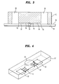
- FIG. 3 shows the mold 10 placed on a microstructure support substrate 28 with the recessed microchannel and micromold cavity structures 16, 18 facing the substrate 28.
- the compliant nature of the mold 10 allows the contact surface 12 to conform to the surface 30 of the substrate 28 producing a plurality of sealed capillary channels 32 which lead into two sealed micromold cavities 34.
- the access openings 20 are also sealed by the conformal contact between the surface 30 of the support substrate 28 and the contact surface 12 of the mold 10.
- the sealed access openings 20 in the mold 10 provide an improved means for introducing the MIMIC solutions into the micromold cavities 34 via the capillary channels 32. Dense, uniform solid microstructures may only be generated from the MIMIC solutions if the micromold cavities 34, via the capillary channels 32, are continuously supplied with the MIMIC solution as the solvent in the solution evaporates This is accomplished with the mold 10 as each access opening 20 functions as a reservoir to maintain a continuous supply of MIMIC solution to a corresponding micromold cavity 34.
- the access openings 20 allow the mold 10 to be filled using conventional automated printing equipment. For example, the access openings 20 can be automatically filled using an ink jet printer or a screen printer (not shown).
- the access openings 20 also eliminate the need to cut away excess material (the material forming the microstructure) which typically remains on the microstructure support substrate when conventional molds without access openings are used. This is because removal of the mold 10 eliminates all material that does not reside in the capillary channels 32, the micromold cavities 34 and at the bottom of the access openings 20.
- the access openings 20 of the mold 10 also enable the MIMIC solution to be applied adjacent the locations where the solution is required and enable the mold 10 to be made with separate micromold cavities 34 which produce separate microstructures. Since each micromold cavity 18 is supplied by its own access opening 20 and set of microchannels 16, each microstructure can be made from a different organic material if desired (using a different solution of organic material).
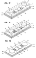
- FIG. 4 shows a mold 10' with a single access opening 20' that supplies two microchannel cavities 18' via two corresponding sets of microchannels 16'.
- FIG. 10 shows a mold 10" having a vacuum ports 60 to evaluate the micromold cavities 34". This in turn draws the MIMIC solution into the mold 10 from the access openings 20".
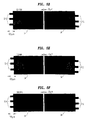
- FIGS. 5A-5F are transmission mode optical micrographs collected at several times after capillary channels and the micromold cavities of the mold 10 in contact with a transparent support, fill with carbon particles from a MIMIC solution of carbon in ethanol (about 2% solids).
- MIMIC solution flows through the two sets of three ⁇ 100 ⁇ m long capillary channels 32 that lead from corresponding access holes (not shown) to corresponding 1 mm by 1 mm micromold cavities 34. The flow stops at the edges of a ⁇ 25 ⁇ m gap.
- Evaporation of the ethanol through the elastomeric mold 10 (PDMS is permeable to ethanol vapor) drives the flow of the solution from the access openings to the micromold cavities 34.
- the time of fabrication can be reduced from about four (4) hours as indicated to about 30 minutes by increasing the solids content of the MIMIC solution.
- FIG. 6 is a profilometer trace collected from three wires formed by one set of the capillary channels.
- the thickness of the carbon wires is slightly less ( ⁇ 5 ⁇ m) than the depth of the recessed microchannel in the mold 10 ( ⁇ 8 ⁇ m).
- the mold 10 may be used in MIMIC to fabricate source and drain electrodes of a plastic field-effect-transistor (FET) from an organic material.
- FET plastic field-effect-transistor
- the FET is first constructed using conventional screen printing processes. Fabrication begins in FIG 7A. by providing a commercially available sheet 40 of poly(ethylene terephthalate) coated with a layer of indium-tin-oxide 42.
- the PET sheet forms a mechanically flexible supporting substrate for the FET.
- the thickness of the PET sheet 40 may be approximately 50 ⁇ m.
- the ITO layer 42 forms a gate electrode for the FET and may be approximately 0.1 ⁇ m thick.
- the FET may also be supported on a mechanically rigid substrate such as silicon having a thickness of approximately 3 mm.
- FIG. 7B shows a layer 44 of pre-imidized polyimide (PI) screen printed onto the ITO layer 42.
- the PI layer 44 forms a thin dielectric approximately less than 1 ⁇ m in thickness.
- Pre-imidized PI is commercially available from Japan Synthetic Rubber Co. under the tradename OPTIMER AL 3046.
- the dielectric layer 44 may also be formed by a 0.1 ⁇ m thick layer of silicon dioxide (SiO 2 ).
- FIG. 7C shows a layer 46 of regioregular poly(3-hexylthiophene) (PHT) screen printed or casted onto the PI dielectric layer 44 using well known methods.
- PHT regioregular poly(3-hexylthiophene)
- the thickness of the PHT layer 46 may be approximately 30-100 nm.
- FIG. 7D shows the mold 10 of FIG. 1 placed onto the PHT layer 46 of the substrate 40 with the recessed microchannels 16 and micromold cavities 18 facing the PHT layer 46.
- the compliant nature of the mold 10 allows it to conformably contact the PHT layer 46 of the substrate 40.
- the mold 10 is located on the substrate so that micromold cavities 18 are disposed directly over the regions of the PHT layer 46 which form the source and drain regions of the FET.
- FIG. 7E shows the access openings 20 of the mold 10 filled with a MIMIC solution 48 containing an organic material.
- the MIMIC solution 48 preferably comprises a carbon paint made up of ethanol solvent and about 2% solid carbon.
- other colloidal suspensions of conductive colloidal particles and conducting polymer solutions may be used for the electrodes.
- the MIMIC solution 48 may also comprise m-cresol solvent and conducting polyaniline (PA).
- PA conducting polyaniline
- the MIMIC solution 48 stored in the openings 20 wicks into the capillary channels 32 and the micromold cavities 34 defined between the PHT layer 46 and the recessed structures 16, 18 of the mold 10. Evaporation of the solvent through the mold 10 from the filled capillary channels 32 and micromold cavities 34 forces the MIMIC solution 48 to flow from the access openings 20 into the capillary channels 32 and the micromold cavities 34.
- the filled access openings 20 of the mold 10 maintain a continuous supply of MIMIC solution 48 in the capillary channels 32 and the microcavities 34.
- FIG. 7F shows the mold removed from the substrate 40
- the mold leaves a pattern 50 of solid carbon on the layer 46 of PHT.
- the pattern 50 includes source and drain electrodes 52, contact pads 54, and wires 56 connecting the contact pads 54 to the electrodes 52.
- FIG. 8 shows a top plan view of the completed FET of FIG. 7F.
- the source and drain electrodes 52 consist of 1mm by 1mm squares separated by about 25 ⁇ m (defining a channel length of ⁇ 25 ⁇ m).
- the contact pads 54 each consist of a 2 mm diameter solid carbon circle.
- the wires 56 connecting the electrodes 52 to the contact pads 54 are each about 100 ⁇ m in length.
- the electrodes and wire structures 52, 56 of the pattern 50 are approximately 5 ⁇ m thick (mold feature depth was ⁇ 8 ⁇ m).
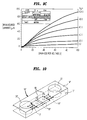
- FIGS. 9A-9C are current-voltage curves from plastic FETs made using the mold of the present invention in MIMIC.
- the scaling of negative drain-source current with negative gate voltages indicates p-channel transistors.
- the field-effect mobilities of these transistors are in the order of 0.01 to 0.05 cm 2 /Vs. These characteristics are consistent with those of larger transistors fabricated using screen printing and conventional photolithographic methods and PHT semiconducting material.
- FIG. 9A shows current-voltage curves of a FET with ⁇ 5 ⁇ m thick conducting carbon electrodes, a ⁇ 50 nm thick semiconducting PHT layer, a screen-printed ⁇ 1 ⁇ m thick PI layer, and an ITO-coated ⁇ 50 ⁇ m thick PET substrate.
- the FET had a channel width of about 2.5 mm, and a channel length of about 25 ⁇ m.
- FIG. 9B shows current-voltage curves of a FET with ⁇ 5 ⁇ m thick conducting carbon electrodes, a ⁇ 50 nm thick semiconducting PHT layer, a ⁇ 0.1 ⁇ m thick SiO 2 layer, and an ITO-coated ⁇ 3 mm thick Si substrate.
- the FET had a channel width of about 2.5 mm, and a channel length of about 25 ⁇ m.
- FIG. 9C shows current-voltage curves of a FET with ⁇ 5 ⁇ m thick doped PA electrodes, a ⁇ 50 nm thick semiconducting PHT layer, a ⁇ 0.1 ⁇ m thick SiO 2 layer, and an ITO-coated ⁇ 3 mm thick Si substrate.
- the FET had a channel width of about 1.0 mm, and a channel length of about 50 ⁇ m.
- the mold of the present invention is capable of producing features as small as 1 ⁇ m in MIMIC.
- the mold can be used with a broad range of materials and when used in MIMIC requires minimal or no access to clean room facilities.
- each access opening in the mold which communicates with a corresponding micromold cavity.
- the syringe can be filled with MIMIC solution which is injected directly into the micromold cavity.
Landscapes
- Engineering & Computer Science (AREA)
- Nanotechnology (AREA)
- Chemical & Material Sciences (AREA)
- Mechanical Engineering (AREA)
- Physics & Mathematics (AREA)
- Manufacturing & Machinery (AREA)
- General Physics & Mathematics (AREA)
- Crystallography & Structural Chemistry (AREA)
- Condensed Matter Physics & Semiconductors (AREA)
- Mathematical Physics (AREA)
- Theoretical Computer Science (AREA)
- Micromachines (AREA)
- Moulds For Moulding Plastics Or The Like (AREA)
- Electroluminescent Light Sources (AREA)
- Electrodes Of Semiconductors (AREA)
- Thin Film Transistor (AREA)
- Casting Or Compression Moulding Of Plastics Or The Like (AREA)
Abstract
Description
Claims (14)
- A method for fabricating a microstructure, the method comprising the steps of(a) providing a substrate for supporting the microstructure;(b) providing an elastomeric mold having first surface and second surfaces, the first surface including at least one recessed microchannel and the second surface including an access opening that extends through the mold to the first surface and communicates with the recessed microchannel;(c) placing the mold onto the substrate with the recessed microchannel facing the substrate;(d) filling the access opening of the mold with a solution including an evaporating solvent and a material, the opening continuously introducing the solution into the microchannel as the solvent of the solution evaporates; and(e) removing the mold from the substrate after the solution evaporates thereby leaving a microstructure formed from the material on the substrate, the microstructure having a shape and dimensions defined by the microchannel.
- A method for fabricating a field-effect transistor, the method comprising the steps of:(a) providing a substrate for supporting the field-effect-transistor; the substrate having a conductive layer disposed thereon;(b) forming a dielectric layer on the conductive layer;(c) forming a semiconducting layer on the dielectric layer;(d) providing an elastomeric mold having first surface and second surfaces, the first surface including at least one recessed microchannel and at least one recessed microcavity communicating with the microchannel and the second surface including a mold filling member that extends through the mold to the first surface and communicates with the recessed microchannel;(e) placing the mold onto the semiconducting layer of the substrate with the recessed microchannel and the recessed microcavity facing the substrate:(f) filling the mold filling member of the mold with a liquid conductive material which is capable of solidifying, the mold filling member continuously introducing the liquid into the microchannel and the microcavity; and(g) removing the mold from the substrate after the liquid solidifies thereby leaving an electrode pattern formed from the solidified conductive material on the substrate, the electrode pattern having a shape and dimensions defined by the microcavity.
- A mold useful in fabricating microstructures. the mold comprising an elastomeric body having a first surface and a second surface, the first surface including at least one recessed microchannel, the second surface including a mold filling member that extends through the mold to the first surface and communicates with the microchannel, wherein the mold filling member allows a liquid material which is capable of solidifying to be continuously introduced into the microchannel thereby forming a microstructure composed of the solidified liquid material having a shape and dimensions defined by the microchannel.
- The method according to claim 1, wherein the substrate includes a plurality of microstructures, for example elements of a microelectronic device.
- The method according to claim 1 or 2, or the mold according to claim 3, wherein the minimum dimension of the microstructure, or electrode pattern, or microchannel is substantially less than 100 µm, for example approximately 0.05 µm.
- The method according to claim 1 or the mold of claim 3, wherein the mold is made from polydimethylsiloxane.
- The method according to claim 1 or 2, or the mold of claim 3, wherein the mold filling member comprises a syringe, or an access opening, that extends through the mold to the first surface and communicates with the recessed microchannel.
- The method according to claim I. wherein the first surface of the mold either includes a recessed microcavity, the microchannel communicating with the filling member and the recessed microcavity, the microstructure formed from the solidified liquid material on the substrate having a shape and dimensions defined by the microchannel and the microcavity; or includes at least a second microchannel communicating with the filling member, the mold filling member continuously introducing the liquid material into the second microchannel during the filling step, whereby a second microstructure formed from the material remains on the substrate after the mold removal step, the second microstructure having a shape and dimensions defined by the second microchannel; or includes at least a second microchannel and the second surface of the mold includes at least a second mold filling member that extends through the mold to the first surface and communicates with the second microchannel, the filling step including filling the second mold filling member with the liquid material, the second mold filling member continuously introducing the liquid material into the second microchannel whereby a second microstructure formed from the solidified liquid material remains on the substrate after the mold removal step, the second microstructure having a shape and dimensions defined by the second microchannel; or includes at least a second microchannel, and the second surface of the mold includes at least a second mold filling member that extends through the mold to the first surface and communicates with the second microchannel, the filling step including the step of filling the second mold filling member with a second liquid material which is capable of solidifying, the second mold filling member continuously introducing the second liquid material into the second microchannel whereby a second microstructure formed from the solidified liquid material remains on the substrate after the mold removal step, the second microstructure having a shape and dimensions defined by the second microchannel.
- The method according to claim 1, further comprising the step of providing at least a second substrate and using the mold provided in step (b) to perform steps (c)-(e) on the second substrate to produce a microstructure on the second substrate.
- The method according to claim 1 or 2, wherein the filling step either includes the step of pressurizing the solution contained within the mold filling member; or includes the step of applying a vacuum to the recessed microchannel to draw the solution from the mold filling member into the microchannel; the filling step for example being performed with an automatic filling device, such as a screen printer or ink jet printer.
- The method according to claim 1 or 2, wherein the material in the liquid material comprises either a colloidal suspension of electrically conductive particles, or a conductive polymer.
- The mold according to claim 3, wherein the first surface of the mold either includes a recessed microcavity, the microchannel extending between the mold filling member and the recessed microcavity, the microstructure formed from the solidified liquid material having a shape and dimensions defined by that of the microchannel and the microcavity; or includes at least a second microchannel communicating with the mold filling member; or includes at least a second microchannel and the second surface of the mold includes at least a second mold filling member extending through the mold to the first surface and communicating with the second microchannel.
- The method according to claim 2, wherein the first surface of the mold includes at least a second microchannel and a second microcavity communicating with the second microchannel and the second surface of the mold includes at least a second mold filling member that extends through the mold to the first surface and communicates with the second microchannel, the filling step including filling the second mold filling member with the liquid material, the second mold filling member continuously introducing the liquid material into the second microchannel whereby the electrode pattern has a shape and dimensions defined by both microcavities.
- The method according to claim 2, wherein the semiconducting layer and/or the dielectric layer, is formed from an organic material. for example a polymeric material, for example formed by silk screening.
Applications Claiming Priority (2)
| Application Number | Priority Date | Filing Date | Title |
|---|---|---|---|
| US49531 | 1998-03-27 | ||
| US09/049,531 US6033202A (en) | 1998-03-27 | 1998-03-27 | Mold for non - photolithographic fabrication of microstructures |
Publications (2)
| Publication Number | Publication Date |
|---|---|
| EP0953420A2 true EP0953420A2 (en) | 1999-11-03 |
| EP0953420A3 EP0953420A3 (en) | 2002-01-16 |
Family
ID=21960314
Family Applications (1)
| Application Number | Title | Priority Date | Filing Date |
|---|---|---|---|
| EP99302016A Withdrawn EP0953420A3 (en) | 1998-03-27 | 1999-03-16 | Mold for non-photolithographic fabrication of microstructures |
Country Status (4)
| Country | Link |
|---|---|
| US (2) | US6033202A (en) |
| EP (1) | EP0953420A3 (en) |
| JP (1) | JP3538335B2 (en) |
| KR (1) | KR100357842B1 (en) |
Cited By (4)
| Publication number | Priority date | Publication date | Assignee | Title |
|---|---|---|---|---|
| EP1864185A4 (en) * | 2005-03-08 | 2011-03-23 | Forskarpatent I Linkoeping Ab | Micro and nano structures in an elastomeric material |
| US7985967B2 (en) | 2002-08-02 | 2011-07-26 | Semiconductor Energy Laboratory Co., Ltd. | Organic thin film transistor and method of manufacturing the same, and semiconductor device having the organic thin film transistor |
| US8343779B2 (en) | 2007-04-19 | 2013-01-01 | Basf Se | Method for forming a pattern on a substrate and electronic device formed thereby |
| WO2013120908A1 (en) * | 2012-02-17 | 2013-08-22 | Sony Dadc Austria Ag | Microstructured polymer devices |
Families Citing this family (90)
| Publication number | Priority date | Publication date | Assignee | Title |
|---|---|---|---|---|
| JP3127889B2 (en) * | 1998-06-25 | 2001-01-29 | 日本電気株式会社 | Manufacturing method of semiconductor package and mold for molding the same |
| US6247986B1 (en) * | 1998-12-23 | 2001-06-19 | 3M Innovative Properties Company | Method for precise molding and alignment of structures on a substrate using a stretchable mold |
| US6517995B1 (en) * | 1999-09-14 | 2003-02-11 | Massachusetts Institute Of Technology | Fabrication of finely featured devices by liquid embossing |
| KR100338329B1 (en) * | 2000-02-25 | 2002-05-27 | 백승준 | Method for forming metal line semiconductor |
| KR100413334B1 (en) * | 2000-03-28 | 2003-12-31 | 주식회사 미뉴타텍 | Method for forming micropattern on substrate by using capillary force |
| WO2002014078A2 (en) | 2000-08-14 | 2002-02-21 | Surface Logix, Inc. | Deformable stamp for patterning three-dimensional surfaces |
| WO2002015264A2 (en) * | 2000-08-18 | 2002-02-21 | Siemens Aktiengesellschaft | Encapsulated organic-electronic component, method for producing the same and use thereof |
| US20040029310A1 (en) * | 2000-08-18 | 2004-02-12 | Adoft Bernds | Organic field-effect transistor (ofet), a production method therefor, an integrated circut constructed from the same and their uses |
| US7186561B2 (en) * | 2000-08-25 | 2007-03-06 | Basf Plant Science Gmbh | Plant polynucleotides encoding novel Na+/H+ antiporters |
| DE10044842A1 (en) * | 2000-09-11 | 2002-04-04 | Siemens Ag | Organic rectifier, circuit, RFID tag and use of an organic rectifier |
| DE10061299A1 (en) * | 2000-12-08 | 2002-06-27 | Siemens Ag | Device for determining and / or forwarding at least one environmental influence, production method and use thereof |
| DE10061297C2 (en) * | 2000-12-08 | 2003-05-28 | Siemens Ag | Procedure for structuring an OFET |
| DE10063721A1 (en) * | 2000-12-20 | 2002-07-11 | Merck Patent Gmbh | Organic semiconductor, manufacturing process therefor and uses |
| WO2002055990A2 (en) * | 2001-01-11 | 2002-07-18 | Musc Foundation For Research Development | Microfabrication process for electrospray ionization mass spectrometry emitters |
| US7090189B2 (en) * | 2001-01-17 | 2006-08-15 | Sandia National Laboratories | Compliant cantilevered micromold |
| DE10105914C1 (en) * | 2001-02-09 | 2002-10-10 | Siemens Ag | Organic field effect transistor with photo-structured gate dielectric and a method for its production |
| US20040094771A1 (en) * | 2001-03-26 | 2004-05-20 | Adolf Bernds | Device with at least two organic electronic components and method for producing the same |
| DE10126859A1 (en) * | 2001-06-01 | 2002-12-12 | Siemens Ag | Production of conducting structures used in organic FETs, illuminated diodes, organic diodes and integrated circuits comprises directly or indirectly forming conducting pathways |
| DE10126860C2 (en) * | 2001-06-01 | 2003-05-28 | Siemens Ag | Organic field effect transistor, process for its manufacture and use for the construction of integrated circuits |
| US6692680B2 (en) | 2001-10-03 | 2004-02-17 | Board Of Supervisors Of Louisiana State University And Agricultural And Mechanical College | Reproduction of micromold inserts |
| EP1441868A4 (en) * | 2001-10-11 | 2006-08-30 | Brewer Science Inc | Patterned structure reproduction using nonsticking mold |
| US20030070569A1 (en) * | 2001-10-11 | 2003-04-17 | Colin Bulthaup | Micro-stencil |
| US6936181B2 (en) * | 2001-10-11 | 2005-08-30 | Kovio, Inc. | Methods for patterning using liquid embossing |
| US20030071016A1 (en) * | 2001-10-11 | 2003-04-17 | Wu-Sheng Shih | Patterned structure reproduction using nonsticking mold |
| DE10151036A1 (en) * | 2001-10-16 | 2003-05-08 | Siemens Ag | Isolator for an organic electronic component |
| DE10151440C1 (en) * | 2001-10-18 | 2003-02-06 | Siemens Ag | Organic electronic component for implementing an encapsulated partially organic electronic component has components like a flexible foil as an antenna, a diode or capacitor and an organic transistor. |
| DE10160732A1 (en) * | 2001-12-11 | 2003-06-26 | Siemens Ag | OFET used e.g. in RFID tag, comprises an intermediate layer on an active semiconductor layer |
| US7229847B2 (en) * | 2002-03-15 | 2007-06-12 | Lucent Technologies Inc. | Forming electrical contacts to a molecular layer |
| US20030235921A1 (en) * | 2002-06-24 | 2003-12-25 | Lucent Technologies Inc. | Forming electrical contacts to a molecular layer |
| DE10212640B4 (en) * | 2002-03-21 | 2004-02-05 | Siemens Ag | Logical components made of organic field effect transistors |
| US7125510B2 (en) * | 2002-05-15 | 2006-10-24 | Zhili Huang | Microstructure fabrication and microsystem integration |
| DE10226370B4 (en) * | 2002-06-13 | 2008-12-11 | Polyic Gmbh & Co. Kg | Substrate for an electronic component, use of the substrate, methods for increasing the charge carrier mobility and organic field effect transistor (OFET) |
| WO2004017439A2 (en) * | 2002-07-29 | 2004-02-26 | Siemens Aktiengesellschaft | Electronic component comprising predominantly organic functional materials and method for the production thereof |
| JP4618990B2 (en) * | 2002-08-02 | 2011-01-26 | 株式会社半導体エネルギー研究所 | ORGANIC THIN FILM TRANSISTOR, MANUFACTURING METHOD THEREOF, AND SEMICONDUCTOR DEVICE HAVING ORGANIC THIN FILM TRANSISTOR |
| US6957608B1 (en) * | 2002-08-02 | 2005-10-25 | Kovio, Inc. | Contact print methods |
| US20060079327A1 (en) * | 2002-08-08 | 2006-04-13 | Wolfgang Clemens | Electronic device |
| US6911385B1 (en) * | 2002-08-22 | 2005-06-28 | Kovio, Inc. | Interface layer for the fabrication of electronic devices |
| CN100338791C (en) | 2002-08-23 | 2007-09-19 | 波尔伊克两合公司 | Organic component for overvoltage protection and associated circuit |
| US6805809B2 (en) | 2002-08-28 | 2004-10-19 | Board Of Trustees Of University Of Illinois | Decal transfer microfabrication |
| US6682331B1 (en) * | 2002-09-20 | 2004-01-27 | Agilent Technologies, Inc. | Molding apparatus for molding light emitting diode lamps |
| US20050167894A1 (en) * | 2002-10-08 | 2005-08-04 | Wu-Sheng Shih | Patterned structure reproduction using nonsticking mold |
| EP1559148A2 (en) * | 2002-11-05 | 2005-08-03 | Siemens Aktiengesellschaft | Organic electronic component with high-resolution structuring and method for the production thereof |
| DE10253154A1 (en) * | 2002-11-14 | 2004-05-27 | Siemens Ag | Biosensor, used to identify analyte in liquid sample, has test field with detector, where detector registers field changes as electrical signals for evaluation |
| DE50306538D1 (en) * | 2002-11-19 | 2007-03-29 | Polyic Gmbh & Co Kg | ORGANIC ELECTRONIC SWITCHING WITH A STRUCTURED SEMICONDUCTIVE FUNCTIONAL LAYER AND MANUFACTURING METHOD THEREFOR |
| US20060035423A1 (en) * | 2002-11-19 | 2006-02-16 | Walter Fix | Organic electronic component comprising the same organic material for at least two functional layers |
| US6872588B2 (en) * | 2002-11-22 | 2005-03-29 | Palo Alto Research Center Inc. | Method of fabrication of electronic devices using microfluidic channels |
| US6759713B2 (en) * | 2002-11-22 | 2004-07-06 | Xerox Corporation | Electronic device structures including interconnecting microfluidic channels |
| DE10300521A1 (en) * | 2003-01-09 | 2004-07-22 | Siemens Ag | Organoresistive memory |
| DE10302149A1 (en) * | 2003-01-21 | 2005-08-25 | Siemens Ag | Use of conductive carbon black / graphite blends for the production of low-cost electronics |
| WO2004066348A2 (en) * | 2003-01-21 | 2004-08-05 | Polyic Gmbh & Co. Kg | Organic electronic component and method for producing organic electronic devices |
| MXPA05007878A (en) * | 2003-01-29 | 2006-02-08 | Polylc Gmbh & Co Kg | Organic storage component and corresponding triggering circuit. |
| US7524409B2 (en) * | 2003-05-15 | 2009-04-28 | University Of Washington | Method and system for electrokinetic, preparative sample separation in high-surface-area separation channels with non-convex cross sections |
| DE10330062A1 (en) * | 2003-07-03 | 2005-01-27 | Siemens Ag | Method and device for structuring organic layers |
| DE10330064B3 (en) * | 2003-07-03 | 2004-12-09 | Siemens Ag | Organic logic gate has load field effect transistor with potential-free gate electrode in series with switching field effect transistor |
| DE10338277A1 (en) * | 2003-08-20 | 2005-03-17 | Siemens Ag | Organic capacitor with voltage controlled capacity |
| DE10339036A1 (en) | 2003-08-25 | 2005-03-31 | Siemens Ag | Organic electronic component with high-resolution structuring and manufacturing method |
| DE10340643B4 (en) * | 2003-09-03 | 2009-04-16 | Polyic Gmbh & Co. Kg | Printing method for producing a double layer for polymer electronics circuits, and thereby produced electronic component with double layer |
| DE10340644B4 (en) * | 2003-09-03 | 2010-10-07 | Polyic Gmbh & Co. Kg | Mechanical controls for organic polymer electronics |
| JP2005183889A (en) * | 2003-12-24 | 2005-07-07 | Konica Minolta Holdings Inc | THIN FILM TRANSISTOR SHEET, METHOD FOR PRODUCING THE SAME, AND THIN FILM TRANSISTOR ELEMENT |
| DE102004002024A1 (en) * | 2004-01-14 | 2005-08-11 | Siemens Ag | Self-aligning gate organic transistor and method of making the same |
| US7909971B2 (en) * | 2004-03-08 | 2011-03-22 | The Board Of Trustees Of The University Of Illinois | Microfluidic electrochemical reactors |
| US7410816B2 (en) * | 2004-03-24 | 2008-08-12 | Makarand Gore | Method for forming a chamber in an electronic device and device formed thereby |
| JP2005321560A (en) * | 2004-05-07 | 2005-11-17 | Fuji Xerox Co Ltd | Polymer optical waveguide module with light receiving/emitting element |
| JP2006011210A (en) * | 2004-06-29 | 2006-01-12 | Fuji Xerox Co Ltd | Polymer optical waveguide module with light emitting element and light receiving element for monitoring |
| DE102004040831A1 (en) | 2004-08-23 | 2006-03-09 | Polyic Gmbh & Co. Kg | Radio-tag compatible outer packaging |
| US20060065361A1 (en) * | 2004-09-30 | 2006-03-30 | Matthias Stiene | Process for manufacturing an analysis module with accessible electrically conductive contact pads for a microfluidic analytical system |
| US20060065532A1 (en) * | 2004-09-30 | 2006-03-30 | Matthias Stiene | Microfluidic analytical system with accessible electrically conductive contact pads |
| US7402616B2 (en) * | 2004-09-30 | 2008-07-22 | Lifescan, Inc. | Fusible conductive ink for use in manufacturing microfluidic analytical systems |
| US7662545B2 (en) * | 2004-10-14 | 2010-02-16 | The Board Of Trustees Of The University Of Illinois | Decal transfer lithography |
| DE102004059465A1 (en) | 2004-12-10 | 2006-06-14 | Polyic Gmbh & Co. Kg | recognition system |
| DE102004059464A1 (en) * | 2004-12-10 | 2006-06-29 | Polyic Gmbh & Co. Kg | Electronic component with modulator |
| DE102004063435A1 (en) | 2004-12-23 | 2006-07-27 | Polyic Gmbh & Co. Kg | Organic rectifier |
| DE102005009820A1 (en) | 2005-03-01 | 2006-09-07 | Polyic Gmbh & Co. Kg | Electronic assembly with organic logic switching elements |
| DE102005009819A1 (en) | 2005-03-01 | 2006-09-07 | Polyic Gmbh & Co. Kg | electronics assembly |
| DE102005017655B4 (en) | 2005-04-15 | 2008-12-11 | Polyic Gmbh & Co. Kg | Multilayer composite body with electronic function |
| WO2007061448A2 (en) * | 2005-05-18 | 2007-05-31 | President And Fellows Of Harvard College | Fabrication of conductive pathways, microcircuits and microstructures in microfluidic networks |
| DE102005031448A1 (en) | 2005-07-04 | 2007-01-11 | Polyic Gmbh & Co. Kg | Activatable optical layer |
| DE102005035589A1 (en) | 2005-07-29 | 2007-02-01 | Polyic Gmbh & Co. Kg | Manufacturing electronic component on surface of substrate where component has two overlapping function layers |
| DE102005044306A1 (en) | 2005-09-16 | 2007-03-22 | Polyic Gmbh & Co. Kg | Electronic circuit and method for producing such |
| EP2005247A2 (en) * | 2006-03-29 | 2008-12-24 | Dow Corning Corporation | Method of forming nanoscale features using soft lithography |
| US20070244258A1 (en) * | 2006-03-29 | 2007-10-18 | Shanti Swarup | Clear coating compositions with improved scratch resistance |
| SG153674A1 (en) * | 2007-12-11 | 2009-07-29 | Nanyang Polytechnic | A method of doping and apparatus for doping |
| EP2966702A4 (en) * | 2013-03-08 | 2016-11-23 | Nat Univ Corp Univ Kobe | METHOD FOR MANUFACTURING ORGANIC SEMICONDUCTOR THIN LAYER |
| US11464451B1 (en) | 2020-03-11 | 2022-10-11 | Huxley Medical, Inc. | Patch for improved biometric data capture and related processes |
| US11660005B1 (en) | 2021-06-04 | 2023-05-30 | Huxley Medical, Inc. | Processing and analyzing biometric data |
| US12178552B1 (en) | 2021-06-04 | 2024-12-31 | Huxley Medical, Inc. | Systems and processes for detecting oxygen saturation and compensating for skin tone variation |
| US12279853B1 (en) | 2021-08-24 | 2025-04-22 | Huxley Medical, Inc. | Photoplethysmography sensors and processes |
| US12114980B1 (en) | 2021-08-24 | 2024-10-15 | Huxley Medical, Inc. | Photoplethysmography sensors and processes |
| US12575741B1 (en) | 2024-04-15 | 2026-03-17 | Huxley Medical, Inc. | Systems and processes for detecting oxygen saturation and compensating for skin tone variation |
| USD1123167S1 (en) | 2024-09-09 | 2026-04-21 | Huxley Medical, Inc. | Wearable medical device |
Family Cites Families (11)
| Publication number | Priority date | Publication date | Assignee | Title |
|---|---|---|---|---|
| US3764248A (en) * | 1971-09-03 | 1973-10-09 | Stewart Rubber Co | Transfer mold for reducing ram flash |
| JPS535255A (en) * | 1976-07-05 | 1978-01-18 | Hitachi Ltd | Mold for molding resin |
| US5071597A (en) * | 1989-06-02 | 1991-12-10 | American Bank Note Holographics, Inc. | Plastic molding of articles including a hologram or other microstructure |
| US5256360A (en) * | 1992-03-25 | 1993-10-26 | Panasonic Technologies, Inc. | Method of manufacturing a precision micro-filter |
| DE4219667C2 (en) * | 1992-06-16 | 1994-12-01 | Kernforschungsz Karlsruhe | Tool and method for producing a microstructured plastic layer |
| JPH06254863A (en) * | 1992-07-06 | 1994-09-13 | Yamatake Control Prod Kk | Forming method of resin product |
| US5538674A (en) * | 1993-11-19 | 1996-07-23 | Donnelly Corporation | Method for reproducing holograms, kinoforms, diffractive optical elements and microstructures |
| DE69509862T2 (en) * | 1994-12-05 | 2000-03-09 | Canon K.K. | Method of manufacturing an ink jet head |
| DE19608667C2 (en) * | 1996-03-06 | 2001-02-15 | Harting Elektrooptische Bauteile Gmbh & Co Kg | Device for molding a microstructure substrate |
| EP0894043B1 (en) * | 1996-03-15 | 2001-10-31 | President And Fellows Of Harvard College | Method of forming articles and patterning surfaces via capillary micromolding |
| US6039897A (en) * | 1996-08-28 | 2000-03-21 | University Of Washington | Multiple patterned structures on a single substrate fabricated by elastomeric micro-molding techniques |
-
1998
- 1998-03-27 US US09/049,531 patent/US6033202A/en not_active Expired - Lifetime
-
1999
- 1999-03-16 EP EP99302016A patent/EP0953420A3/en not_active Withdrawn
- 1999-03-24 KR KR1019990009959A patent/KR100357842B1/en not_active Expired - Lifetime
- 1999-03-26 JP JP08388899A patent/JP3538335B2/en not_active Expired - Fee Related
- 1999-09-09 US US09/393,032 patent/US6322736B1/en not_active Expired - Lifetime
Cited By (6)
| Publication number | Priority date | Publication date | Assignee | Title |
|---|---|---|---|---|
| US7985967B2 (en) | 2002-08-02 | 2011-07-26 | Semiconductor Energy Laboratory Co., Ltd. | Organic thin film transistor and method of manufacturing the same, and semiconductor device having the organic thin film transistor |
| US8368065B2 (en) | 2002-08-02 | 2013-02-05 | Semiconductor Energy Laboratory Co., Ltd. | Organic thin film transistor and method of manufacturing the same, and semiconductor device having the organic thin film transistor |
| EP1864185A4 (en) * | 2005-03-08 | 2011-03-23 | Forskarpatent I Linkoeping Ab | Micro and nano structures in an elastomeric material |
| US8343779B2 (en) | 2007-04-19 | 2013-01-01 | Basf Se | Method for forming a pattern on a substrate and electronic device formed thereby |
| WO2013120908A1 (en) * | 2012-02-17 | 2013-08-22 | Sony Dadc Austria Ag | Microstructured polymer devices |
| US9823221B2 (en) | 2012-02-17 | 2017-11-21 | STRATEC CONSUMABLES GmbH | Microstructured polymer devices |
Also Published As
| Publication number | Publication date |
|---|---|
| KR100357842B1 (en) | 2002-10-25 |
| JP3538335B2 (en) | 2004-06-14 |
| EP0953420A3 (en) | 2002-01-16 |
| JPH11330004A (en) | 1999-11-30 |
| KR19990078180A (en) | 1999-10-25 |
| US6033202A (en) | 2000-03-07 |
| US6322736B1 (en) | 2001-11-27 |
Similar Documents
| Publication | Publication Date | Title |
|---|---|---|
| US6322736B1 (en) | Method for fabricating molded microstructures on substrates | |
| KR100870250B1 (en) | A method of forming an electronic device, an electronic device formed by the method, a logic circuit including the electronic device, a display and a memory, and a microcutting tool used to form the electronic device. | |
| Menard et al. | Micro-and nanopatterning techniques for organic electronic and optoelectronic systems | |
| EP1581973B1 (en) | A method of manufacturing an electronic device | |
| US6966997B1 (en) | Methods for patterning polymer films, and use of the methods | |
| Parashkov et al. | Large area electronics using printing methods | |
| US6736985B1 (en) | High-resolution method for patterning a substrate with micro-printing | |
| US8372731B2 (en) | Device fabrication by ink-jet printing materials into bank structures, and embossing tool | |
| US20040013982A1 (en) | Fabrication of finely featured devices by liquid embossing | |
| EP1422766A2 (en) | Method of fabrication of electronic devices using microfluidic channels | |
| US9401306B2 (en) | Self-aligned capillarity-assisted microfabrication | |
| WO2004083843A1 (en) | Electrochemical microfluidic sensor and method of creation of its microchannels by embossing | |
| KR100675632B1 (en) | Pattern Forming Method and Manufacturing Method of Liquid Crystal Display Using The Same | |
| US7582509B2 (en) | Micro-embossing fabrication of electronic devices | |
| US20090152540A1 (en) | Semiconductor device and process for producing same | |
| US20040099911A1 (en) | Novel electronic device structures including interconnecting microfluidic channels | |
| US20070052019A1 (en) | Transistor device wiwth metallic electrodes and a method for use in forming such a device | |
| KR20090065896A (en) | Film substrate with a fine circuit and a manufacturing method therefor | |
| US20060240668A1 (en) | Semiconductor device with metallic electrodes and a method for use in forming such a device | |
| Moonen | Alternative lithography strategies for flexible electronics | |
| JP2006186293A (en) | Thin film transistor manufacturing method | |
| Rogers et al. | Large area, rubber stamped plastic circuits for electronic paper | |
| Mahajan | New Approaches for Printed Electronics Manufacturing | |
| Jo et al. | Roll-printed organic thin-film transistor using patterned poly (dimethylsiloxane)(PDMS) stamp | |
| Rogers et al. | Rubber stamped plastic circuits for electronic paper |
Legal Events
| Date | Code | Title | Description |
|---|---|---|---|
| PUAI | Public reference made under article 153(3) epc to a published international application that has entered the european phase |
Free format text: ORIGINAL CODE: 0009012 |
|
| AK | Designated contracting states |
Kind code of ref document: A2 Designated state(s): AT BE CH CY DE DK ES FI FR GB GR IE IT LI LU MC NL PT SE Kind code of ref document: A2 Designated state(s): DE FR GB |
|
| AX | Request for extension of the european patent |
Free format text: AL;LT;LV;MK;RO;SI |
|
| PUAL | Search report despatched |
Free format text: ORIGINAL CODE: 0009013 |
|
| AK | Designated contracting states |
Kind code of ref document: A3 Designated state(s): AT BE CH CY DE DK ES FI FR GB GR IE IT LI LU MC NL PT SE |
|
| AX | Request for extension of the european patent |
Free format text: AL;LT;LV;MK;RO;SI |
|
| RIC1 | Information provided on ipc code assigned before grant |
Free format text: 7B 29C 39/00 A, 7H 01L 21/00 B, 7B 29C 39/24 B, 7B 29C 33/40 B, 7B 29C 33/42 B |
|
| 17P | Request for examination filed |
Effective date: 20020716 |
|
| AKX | Designation fees paid |
Free format text: DE FR GB |
|
| 17Q | First examination report despatched |
Effective date: 20040310 |
|
| STAA | Information on the status of an ep patent application or granted ep patent |
Free format text: STATUS: THE APPLICATION IS DEEMED TO BE WITHDRAWN |
|
| 18D | Application deemed to be withdrawn |
Effective date: 20040721 |