EP0953152B1 - Gas-sensing semiconductor devices - Google Patents
Gas-sensing semiconductor devices Download PDFInfo
- Publication number
- EP0953152B1 EP0953152B1 EP98900594A EP98900594A EP0953152B1 EP 0953152 B1 EP0953152 B1 EP 0953152B1 EP 98900594 A EP98900594 A EP 98900594A EP 98900594 A EP98900594 A EP 98900594A EP 0953152 B1 EP0953152 B1 EP 0953152B1
- Authority
- EP
- European Patent Office
- Prior art keywords
- gas
- layer
- mosfet
- sensitive layer
- sensing area
- Prior art date
- Legal status (The legal status is an assumption and is not a legal conclusion. Google has not performed a legal analysis and makes no representation as to the accuracy of the status listed.)
- Expired - Lifetime
Links
Images




Classifications
-
- G—PHYSICS
- G01—MEASURING; TESTING
- G01N—INVESTIGATING OR ANALYSING MATERIALS BY DETERMINING THEIR CHEMICAL OR PHYSICAL PROPERTIES
- G01N27/00—Investigating or analysing materials by the use of electric, electrochemical, or magnetic means
- G01N27/02—Investigating or analysing materials by the use of electric, electrochemical, or magnetic means by investigating impedance
- G01N27/04—Investigating or analysing materials by the use of electric, electrochemical, or magnetic means by investigating impedance by investigating resistance
- G01N27/12—Investigating or analysing materials by the use of electric, electrochemical, or magnetic means by investigating impedance by investigating resistance of a solid body in dependence upon absorption of a fluid; of a solid body in dependence upon reaction with a fluid, for detecting components in the fluid
- G01N27/128—Microapparatus
Definitions
- This invention relates to gas-sensing semiconductor devices for detecting the presence and/or concentration of one or more gases.
- WO 95/19563 discloses a gas sensor comprising a semiconductor substrate formed with a recessed well, a membrane made of silicon-containing oxide and/or nitrate layers and covering the well, an insulating cover layer attached to the membrane, and a thin-film heater and thin-film comb electrodes attached to the membrane cover layer and covered by a tin-oxide sensor layer.
- the sensor layer serves as an indirectly heated thin-film resistor which is sensitive to a gas atmosphere so that the output from the comb electrodes can be used for determining the presence of an appropriate gas, such as propane.
- propane propane
- US-A-4 502 938 and US-A-4 878 015 both disclose gas-sensing semiconductor devices each comprising a chemical-responsive FET formed in a silicon substrate (bulk).
- a gas-sensing semiconductor device comprising a semiconductor substrate, a thin insulating layer on one side of the substrate, and a thin semiconductor layer on top of the thin insulating layer, wherein the device includes at least one sensing area in which the material of the substrate has been removed to leave a membrane formed by the thin insulating layer and the thin semiconductor layer, and wherein the or each sensing area is provided with a gas-sensitive layer and a heater for heating the gas-sensitive layer to promote gas reaction with the gas-sensitive layer, and a sensor for providing an electrical output indicative of gas reaction with the gas-sensitive layer, characterised in that the or each sensing area incorporates a MOSFET formed in the thin semiconductor layer and forming part of the heater and/or sensor.
- Such a gas-sensing semiconductor device can be produced so as to have very low power consumption using a series of fabrication steps compatible with known CMOS SOI (silicon on insulator) technology for integrated circuits. As compared with conventional planar integrated gas sensors, this considerably simplifies the fabrication of the device, and thus decreases the manufacturing cost. Furthermore the device may be integrated with processing circuitry, such as a processor unit and a driving circuit, on a single chip so as to produce a "smart" gas microsensor. Unlike in conventional gas microsensors, the heater can be produced without requiring any fabrication steps in addition to those already employed in the IC processing. The use of SOI technology also allows accurate bipolar temperature sensors to be integrated into the device.
- CMOS SOI silicon on insulator
- CMOS SOI integrated circuits may be fabricated by forming a thin layer of insulating material, such as silicon oxide, on the semiconductor substrate followed by forming of a thin silicon layer on top of the insulating layer.
- insulating material such as silicon oxide
- Other insulating materials can be used in place of silicon oxide, such as silicon nitride or a combination of silicon oxide and silicon nitride.
- Individual semiconductor devices, such as MOSFET's, are then fabricated within the thin silicon layer using known fabrication steps.
- SOI technology results in high speed/low power CMOS performance, as well as providing simple and efficient device isolation, reduced parasitic capacitances, latch-up elimination and reduced short-channel effects.
- fully depleted devices (with an ultra-thin SOI layer) have been reported to have attractive features. They do not exhibit kink phenomena, have a sharp sub-threshold slope, and are stable in terms of dynamic floating body effects relating to impact-ionisation and charge-pumping phenomena.
- the SOI transistors also possess a lower off-state leakage current by a factor of about 10-100 when compared with conventional bulk silicon devices. This is important in reducing the stand-by power dissipation.
- SOI technology enables device operation at higher temperatures than conventional devices, mainly due to reduced leakage currents.
- the sensing area comprises a membrane formed by the thin insulating layer and the top thin semiconductor layer after removal of the substrate material, for example using a standard anisotropic back-etching process.
- the thin insulating layer of silicon oxide for example, which is part of the standard SOI structure, serves a dual purpose, namely (i) it acts as an etch stop in the sensing area and thermally isolates the sensing area so as to reduce power losses at high temperatures, and (ii) it provides high grade electrical isolation from any associated integrated circuit area, incorporating transducer and associated processing circuitry for example, as well as providing reduced interferences, latch-up elimination and reduced capacitances in the specific case of low power CMOS SOI integrated circuits.
- a gas microsensor array device can be built by integrating several individual sensor cells utilising different gas-sensitive layers in the same chip. The individual sensor cells can be built on the same membrane or can have separate membranes. Such a microsensor array device possesses the advantages over individual sensors of improved gas selectivity, lower noise and reduced effect of poisoning through superior structural design or signal processing.
- gas-sensing semiconductor device in accordance with the invention to be described with reference to the drawings are fabricated utilising CMOS SOI technology so as to provide gas sensing areas integrated with IC circuitry in a single chip, each sensing area being a thin membrane formed by a thin insulating layer and a thin semiconductor layer.
- the thin insulating layer which provides thermal isolation, may be an oxide, a nitride, a combination of oxide and nitride or some other insulating material.
- Particular attention is drawn in the accompanying description to the fabrication of the device in the sensing areas, although it will be understood that IC fabrication will be effected simultaneously to provide the associated circuitry in other areas of the device.
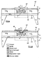
- the device 1 is fabricated on a silicon substrate 2 having a thin silicon oxide insulating layer 3 on one side, and a thin silicon layer 4 on top of the insulating layer 3.
- the silicon layer 4 is in the form of an island surrounded by a silicon oxide insulating barrier layer 5 formed by the known LOCOS oxidation technique so as to extend vertically to substantially meet the thin insulating layer 3.
- the LOCOS oxidation technique has the advantage of producing both efficient lateral electrical isolation in the sensing area and the associated electronic IC areas, and also thermally insulating the sensing area.
- the thermal oxide has a much lower thermal conductivity than the silicon and therefore the thermal power losses in the sensing area will be greatly reduced.
- lateral isolation techniques such as MESA etching of the thin silicon layer, trench isolation (trenches filled with oxide or other insulating material) or SIMOX TDI (separation by implanted oxygen to provide total dielectric isolation), may also be used in a similar way.
- a MOSFET heater 6 is formed in the sensing area by known CMOS SOI or Bi-CMOS SOI processing and comprises a n+ source layer 7 and a n-drain layer 8 diffused in the lowly doped p-type ⁇ silicon layer 4.
- the heater 6 is shown as an n-type MOSFET, it will be appreciated that a p-type MOSFET heater could also be employed.
- a silicon oxide layer 10 is grown at the surface to form the gate oxide followed by the deposition and patterning of a polysilicon layer 11 on top of the gate oxide.
- the n+ source layer 7 and n+ drain layer 8 are further implanted and could be self-aligned to the gate and LOCOS barrier layer 5.
- a metalisation layer 9 is applied and patterned on top of the source and drain diffusions.
- the pads for the source, drain and gate contacts (not shown) are placed outside the membrane area to avoid thermal and mechanical stress.
- a further silicon oxide layer 12 is applied to the gate, and a passivation layer 14 is deposited in a manner compatible with conventional SOI technology.
- the passivation layer 14 may be an oxide and/or nitride layer or a thin glass layer, although other passivation layers, such as amorphous materials and polyimide, are possible.
- the same processing steps are used to fabricate the low power transistors in the electronic IC areas.
- a chemoresistor sensor 16 is fabricated in the sensing area by depositing a metallisation layer 17 on top of the passivation layer 14 to form two spaced electrodes and by subsequently placing a gas-sensitive layer 18 made either of an inorganic material (such as tin oxide) or an organic material (such as a polymer or pthalocyanine) so as to span the two electrodes.
- the gas-sensitive layer 18 can be deposited by sputtering etc. or can be electrochemically grown onto the two electrodes (as in the case of conducting polymers).
- the substrate 2 is back-etched so as to form the thin membrane 20 in the sensing area, with the insulating layer 3 serving to stop the back-etching.
- Either a single chemoresistor sensor 16 or an array of chemoresistors may be provided on top of the heater 6, the or each chemoresistor comprising a layer of inorganic or organic material. In a different design the chemoresistor can be disposed laterally and surrounded by the MOSFET heater.
- CMOS or Bi-CMOS integrated temperature sensor (not shown) can be fabricated in the sensing area adjacent to the gas-sensitive layer 18.
- a temperature sensor may comprise unipolar or bipolar devices formed by SOI technology and may make use of variation of the emitter-base voltage with temperature. Such temperature sensors are widely used and give accurate results.
- the MOSFET heater 6 may have an interdigitated structure to uniformly heat the sensing area, and there is no need for deposition of special metal layers, of platinum or NiFe for example, to form a conventional metallic heater resistor. If the sensor comprises an array of individual sensor cells, a single common heater may be used for all the sensor cells, or alternatively an array of MOSFET heaters may be employed. If required, such a heater array could be adapted to heat different sensor cells to different temperatures, in which case the source diffusion could be common to all the heaters (or the sources of all the heaters could be connected together by a metal layer) and connected to a fixed voltage, such as ground for example.
- drain diffusion could be common to all the heaters (or the drains of all the heaters could be connected together by a metal layer) and connected to a fixed potential, such as 3V for example.
- the gate terminals of the heaters must remain separate, however, so that, by applying different voltages to the gates of the heaters, different power levels can be established and thus different temperatures can be developed across the sensing area.
- a desired temperature gradient or temperature pattern that is an uneven temperature distribution, can also be developed across part of the sensing area by controlling the channel length of a MOSFET heater. At given drain, source and gate potentials, a longer channel length results in a lower channel current and thus in less power being dissipated.
- MOSFET heaters also drastically simplifies the driving circuitry since, because of the high input impedance of the gate, a MOSFET heater can be controlled by digital circuits or operational amplifiers. Temperature cycles can be applied across the sensing area by driving the MOSFET heaters with digital or analogue switching devices. Furthermore, if required, the gas-sensitive layer could be cleaned to remove gas impurities by applying a voltage higher than the normal operating voltage to the gate of the or each heater in a clean atmosphere, so as to cause any contaminating compounds to be driven out of the gas-sensitive layer by the very high temperatures developed.
- Figure 2 shows the sensing area of Figure 1a together with an associated electronic IC area of the same device 1, and shows in particular the fabrication of an n-type MOSFET 22 and a p-type MOSFET 24 formed in the IC area of the substrate by the same processing steps to those used in the fabrication of the sensing area as described above, with reference to Figure 1(a).
- Figure 1b shows a variation of the structure of Figure 1a in which a device 1' comprises a similar thin insulating layer 3 and silicon layer 4 on a substrate 2, as in Figure 1a except that the silicon layer 4 is not fully depleted during on-state operation of the MOSFET, so that the silicon layer 4 is thicker than in the previous case.
- This is known as non-fully depleted CMOS SOI technology.
- Lateral isolation (not shown) can employ, for example, junction isolation structure, trench oxidation, MESA etching or, for relatively thinner silicon layers, LOCOS oxidation.
- a p+ layer 26 is provided to avoid parasitic conduction between individual cells of the device.
- Figure 3 shows the sensing area of such a device, together with an associated electronic IC area formed by the same processing steps.
- the senor may be formed by a MOSFET having a gate formed by the gas-sensitive layer and a thin gate oxide, as described more fully below.
- the gas-sensitive layer may be made of organic material, such as a conductive polymer, or inorganic conductive material, such as a metal oxide.
- the MOSFET heater 42 is also used as the sensing element, and incorporates a gas-sensitive layer 43 which is applied to the gate on top of the silicon oxide layer 10.
- the gas-sensitive layer 43 may be made of an organic conductive material, such as a conjugated polymer.
- the nature of the gas detected and/or its concentration can be determined by monitoring the change in the channel threshold current or sub-threshold current in the presence of the gas, by comparison of the I-V characteristics in the presence of the gas with the I-V characteristics in the absence of the gas, or by directly detecting the threshold voltage.
- This particular structure can be used for relatively low temperatures (below 100C) and the temperature can be adjusted by varying the drain-source voltage.
- the device 44 of Figure 4b is a variation of the device 40 of Figure 4a in which the gas-sensitive layer 43 is made of an inorganic semiconducting material, such as a catalytically doped metal oxide, and a porous metal layer 45, made of gold for example, is deposited on top of the gas-sensitive layer 43 to form a controllable gate.
- the porous metal layer 45 allows the gas to diffuse through to the gas-sensitive layer 43.
- the MOSFET acts as a heater with the desired temperature being set by the drain and gate potentials so that the heater is controllable in a similar manner to the heater of Figure 1a, except that the MOSFET also constitutes the sensing element in Figure 4b.
- the work function of the gas-sensitive layer 43 changes and therefore the threshold voltage of the MOSFET changes. Since the gate voltage is much higher than the change in the threshold voltage, this will not significantly affect the power dissipated, and thus the temperature.
- the change in the current or voltage due to the variation of the work function in the presence of the gas at a given temperature, that is at a given MOSFET bias point can be detected by a highly accurate integrated CMOS or Bi-CMOS transducer.
- the porous layer is also the gas-sensitive layer, being made of a thin film of catalytic metal, such as palladium or iridium for example.
- catalytic metal film could not be produced by standard CMOS technology and would need to be sputtered down as a final process or via lift-off.
- Figures 5a and 5b show variations 50 and 54 of the structures of Figures 4a and 4b respectively in which an additional heater is provided by a heater resistor 52 in the form of a resistive layer, of platinum or NiFe for example, deposited on the back side of the membrane 20 and connected to two electrodes.
- the structure can be heated up by applying a voltage drop across the heater resistor 52, and the temperature can be monitored by detecting the change of the heater resistance with current.
- Figures 6a and 6b show variations 60 and 64 of the structures of Figures 4a and 4b respectively in which a metal gate electrode 62 is deposited on the back side of the membrane 20 after back-etching, in order to control the heater current flowing through the back side of the MOSFET.
- the structures of Figures 6a and 6b can be considered as incorporating a back-side MOSFET heater. This is only possible when the source and drain diffusions reach the thin insulating layer 3.
- a back channel is formed between the source and the drain at the interface between the thin insulating layer 3 and the silicon layer 4.
- the sensing MOSFET operates in parallel with the back-side heater MOSFET so that there are two MOSFET channel paths from source to drain arranged in parallel.
- both the sensing/heater MOSFET and the back heater MOSFET participate in heating, and therefore the temperature is controlled by the voltage applied to the two parallel gates.
- a sensing MOSFET and heater MOSFET are disposed laterally adjacent one another in the sensing area.
- sensing MOSFET's can be used to form a sensor array. and the layout design may consist of alternate sensing MOSFET's and heater MOSFET's. Alternatively sensing MOSFET's may be alternated with conventional heaters.
- Figures 7a, 7b and 7c show variations 80, 84 and 86 in which a chemoresistor sensor 82 and a heater MOSFET 83 are disposed laterally adjacent one another in the sensing area.
- the chemoresistor sensor 82 can be formed on the thin insulating layer 3 ( Figure 7a), on the passivation layer 14 ( Figure 7b) or on the silicon barrier layer 5 ( Figure 7c).
- the above structures can also be used as microcalorimeters (or as both chemoresistors and microcalorimeters) in which the additional heat liberated or absorbed by the gas-sensitive layer in the presence of the gas is detected.
- the temperature of the sensing material changes as a result of its reaction with the gas so that the nature of the gas and/or its concentration can be determined by monitoring the heat liberated or absorbed by the gas-sensitive layer in the presence of the gas.
- An appropriate gas-sensitive layer for such an application would be a non-electrically conducting material such as gamma-alumina (pellistor).
- Chemoresistive materials such as tin oxide change their thermal conductivity so that it is possible to monitor the change in thermal conductivity, the heat liberated and the change in the electrical conductivity at high temperatures. This is an attractive technique in SOI MOSFET devices because of the very fast thermal response permitting rapid measurements.
Landscapes
- Chemical & Material Sciences (AREA)
- Chemical Kinetics & Catalysis (AREA)
- Electrochemistry (AREA)
- Physics & Mathematics (AREA)
- Health & Medical Sciences (AREA)
- Life Sciences & Earth Sciences (AREA)
- Analytical Chemistry (AREA)
- Biochemistry (AREA)
- General Health & Medical Sciences (AREA)
- General Physics & Mathematics (AREA)
- Immunology (AREA)
- Pathology (AREA)
- Investigating Or Analyzing Materials By The Use Of Fluid Adsorption Or Reactions (AREA)
- Investigating Or Analyzing Materials By The Use Of Electric Means (AREA)
- Thin Film Transistor (AREA)
Abstract
Description
Claims (17)
- A gas-sensing semiconductor device comprising a semiconductor substrate (2), a thin insulating layer (3) on one side of the substrate, and a thin semiconductor layer (4) on top of the thin insulating layer, wherein the device includes at least one sensing area in which the material of the substrate has been removed to leave a membrane (20) formed by the thin insulating layer and the thin semiconductor layer, and wherein the or each sensing area is provided with a gas-sensitive layer (18, 43) and a heater (6, 42, 52, 62, 83) for heating the gas-sensitive layer to promote gas reaction with the gas-sensitive layer, and a sensor (16, 42, 82) for providing an electrical output indicative of gas reaction with the gas-sensitive layer, characterised in that the or each sensing area incorporates a MOSFET formed in the thin semiconductor layer (4) and forming part of the heater and/or sensor.
- A device according to claim 1, wherein the heater (6, 42, 52, 62, 83) incorporates said MOSFET in the vicinity of the gas-sensitive layer (18, 43).
- A device according to claim 1 or 2, wherein the gas-sensitive layer (18, 43) is incorporated in the gate of said MOSFET so that the threshold of the MOSFET changes in response to gas reaction with the gas-sensitive layer.
- A device according to claim 3, wherein the gate comprises a conductive polymer layer which acts as the gas-sensitive layer.
- A device according to any preceding claim, wherein a gate electrode (62) is applied to the back side of the thin insulating layer (3) in order to control a heating current in said MOSFET.
- A device according to any preceding claim, wherein a gas-permeable metal layer (45) is applied on top of the gas-sensitive layer (18, 43) to allow gas to diffuse through the gas-permeable metal layer towards the gas-sensitive layer.
- A device according to any preceding claim, wherein the sensor (16, 42, 82) incorporates at least said MOSFET in the vicinity of the gas-sensitive layer (18, 43).
- A device according to any preceding claim, which has been produced utilising CMOS SOI or bi-CMOS SOI fabrication steps.
- A device according to any preceding claim, wherein the heater incorporates a heater resistor (52) applied to the back side of the thin insulating layer (3) in the or each sensing area.
- A device according to any preceding claim, wherein the gas-sensitive layer (18) incorporates part of a chemoresistor sensor (16, 82).
- A device according to any preceding claim, wherein the or each sensing area incorporates temperature sensing means.
- A device according to claim 11, wherein the temperature sensing means comprises at least one bipolar transistor.
- A device according to any preceding claim, wherein said MOSFET is a fully depleted MOSFET in the thin semiconductor layer (4) laterally isolated by LOCOS oxidation.
- A device according to any preceding claim, wherein. the sensing area incorporates more than one said MOSFET formed in the thin semiconductor layer (4), the MOSFET's forming a heater (83) and a sensor (82) adjacent one another in the thin semiconductor layer (4).
- A device according to any preceding claim, wherein the material of the substrate (2) has been removed in at least one sensing area by back etching.
- A device according to any preceding claim, wherein the thin insulating layer (3) is of silicon oxide and the thin semiconductor layer (4) is of silicon.
- A device according to any preceding claim, wherein the or each sensing area is integrated with at least one electronic circuit area incorporating associated circuitry (22, 24).
Applications Claiming Priority (3)
| Application Number | Priority Date | Filing Date | Title |
|---|---|---|---|
| GB9700723 | 1997-01-15 | ||
| GB9700723A GB2321336B (en) | 1997-01-15 | 1997-01-15 | Gas-sensing semiconductor devices |
| PCT/GB1998/000100 WO1998032009A1 (en) | 1997-01-15 | 1998-01-13 | Gas-sensing semiconductor devices |
Publications (2)
| Publication Number | Publication Date |
|---|---|
| EP0953152A1 EP0953152A1 (en) | 1999-11-03 |
| EP0953152B1 true EP0953152B1 (en) | 2002-05-22 |
Family
ID=10806000
Family Applications (1)
| Application Number | Title | Priority Date | Filing Date |
|---|---|---|---|
| EP98900594A Expired - Lifetime EP0953152B1 (en) | 1997-01-15 | 1998-01-13 | Gas-sensing semiconductor devices |
Country Status (7)
| Country | Link |
|---|---|
| US (1) | US6111280A (en) |
| EP (1) | EP0953152B1 (en) |
| AT (1) | ATE217967T1 (en) |
| AU (1) | AU5568598A (en) |
| DE (1) | DE69805500T2 (en) |
| GB (1) | GB2321336B (en) |
| WO (1) | WO1998032009A1 (en) |
Cited By (3)
| Publication number | Priority date | Publication date | Assignee | Title |
|---|---|---|---|---|
| DE102005010032A1 (en) * | 2005-03-04 | 2006-09-07 | Siemens Ag | Gas-sensitive field-effect transistor, operating method and use |
| DE102010041763A1 (en) | 2010-09-30 | 2012-04-05 | Siemens Aktiengesellschaft | Micromechanical substrate |
| US20130327944A1 (en) * | 2011-01-21 | 2013-12-12 | Excelitas Technologies Singapore PTE, Ltd. | Heated radiation sensor |
Families Citing this family (114)
| Publication number | Priority date | Publication date | Assignee | Title |
|---|---|---|---|---|
| KR100267013B1 (en) | 1998-05-27 | 2000-09-15 | 윤종용 | A semiconductor device and method of the fabricating same |
| FR2795821B1 (en) * | 1999-07-02 | 2001-09-14 | Microchemical Systems S A | CHEMICAL SENSOR OF METAL OXIDE GAS AND MANUFACTURING METHOD THEREOF |
| DE60004843T2 (en) * | 1999-07-02 | 2004-06-03 | Microchemical Systems S.A. | METAL OXIDE CHEMICAL GAS SENSOR AND RELATED PRODUCTION METHOD |
| US6418784B1 (en) * | 1999-10-08 | 2002-07-16 | Ford Global Technologies, Inc. | Combined combustible gas sensor and temperature detector |
| DE10006237A1 (en) * | 2000-02-11 | 2001-08-23 | Siemens Ag | Gas sensitive FET |
| FR2812723B1 (en) | 2000-08-01 | 2002-11-15 | Centre Nat Rech Scient | SENSOR OF REDUCING GAS MOLECULES |
| CN1233041C (en) | 2000-09-21 | 2005-12-21 | 剑桥半导体有限公司 | Semiconductor device and method of forming a semiconductor device |
| GB2371922B (en) * | 2000-09-21 | 2004-12-15 | Cambridge Semiconductor Ltd | Semiconductor device and method of forming a semiconductor device |
| RU2196981C2 (en) * | 2000-11-20 | 2003-01-20 | Саито Такеши | Gas-sensitive pickup |
| EP1360478A1 (en) * | 2000-12-20 | 2003-11-12 | Eidgenössische Technische Hochschule Zürich | Microsensor and single chip integrated microsensor system |
| GB2370410A (en) * | 2000-12-22 | 2002-06-26 | Seiko Epson Corp | Thin film transistor sensor |
| CN100459163C (en) * | 2001-02-19 | 2009-02-04 | 国际商业机器公司 | Thin film transistor structure, manufacturing method thereof, and display device using same |
| US6580600B2 (en) | 2001-02-20 | 2003-06-17 | Nippon Soken, Inc. | Capacitance type humidity sensor and manufacturing method of the same |
| US20020167003A1 (en) * | 2001-04-18 | 2002-11-14 | Campbell Ian H. | Chemical and biological sensor using organic self-assembled transitors |
| DE10121262A1 (en) * | 2001-04-30 | 2002-11-14 | Siemens Ag | Device for the quantitative measurement of nitrogen oxides in exhaled air and use |
| KR100401377B1 (en) * | 2001-07-09 | 2003-10-17 | 엘지.필립스 엘시디 주식회사 | Liquid Crystal Display Device and Driving Method for the same |
| JP4501320B2 (en) * | 2001-07-16 | 2010-07-14 | 株式会社デンソー | Capacitive humidity sensor |
| JP4325133B2 (en) * | 2001-08-27 | 2009-09-02 | 株式会社デンソー | Gas sensor and manufacturing method thereof |
| US20030116552A1 (en) * | 2001-12-20 | 2003-06-26 | Stmicroelectronics Inc. | Heating element for microfluidic and micromechanical applications |
| US6504226B1 (en) * | 2001-12-20 | 2003-01-07 | Stmicroelectronics, Inc. | Thin-film transistor used as heating element for microreaction chamber |
| US8152991B2 (en) | 2005-10-27 | 2012-04-10 | Nanomix, Inc. | Ammonia nanosensors, and environmental control system |
| US8154093B2 (en) | 2002-01-16 | 2012-04-10 | Nanomix, Inc. | Nano-electronic sensors for chemical and biological analytes, including capacitance and bio-membrane devices |
| US20050279987A1 (en) * | 2002-09-05 | 2005-12-22 | Alexander Star | Nanostructure sensor device with polymer recognition layer |
| DE10210819B4 (en) * | 2002-03-12 | 2004-04-15 | Micronas Gmbh | Microstructured gas sensor with control of the gas sensitive properties by applying an electric field |
| US7547931B2 (en) * | 2003-09-05 | 2009-06-16 | Nanomix, Inc. | Nanoelectronic capnometer adaptor including a nanoelectric sensor selectively sensitive to at least one gaseous constituent of exhaled breath |
| US20070048181A1 (en) * | 2002-09-05 | 2007-03-01 | Chang Daniel M | Carbon dioxide nanosensor, and respiratory CO2 monitors |
| US20070048180A1 (en) * | 2002-09-05 | 2007-03-01 | Gabriel Jean-Christophe P | Nanoelectronic breath analyzer and asthma monitor |
| US7522040B2 (en) * | 2004-04-20 | 2009-04-21 | Nanomix, Inc. | Remotely communicating, battery-powered nanostructure sensor devices |
| US6627959B1 (en) | 2002-04-16 | 2003-09-30 | Boston Microsystems, Inc. | P-n junction sensor |
| DE10219726A1 (en) * | 2002-05-02 | 2003-11-27 | Eads Deutschland Gmbh | Production of a bridge-like semiconductor gas sensor comprises preparing a SOI element, forming an electrode arrangement on an electrically insulating layer |
| US7948041B2 (en) * | 2005-05-19 | 2011-05-24 | Nanomix, Inc. | Sensor having a thin-film inhibition layer |
| US20060263255A1 (en) * | 2002-09-04 | 2006-11-23 | Tzong-Ru Han | Nanoelectronic sensor system and hydrogen-sensitive functionalization |
| US20070114573A1 (en) * | 2002-09-04 | 2007-05-24 | Tzong-Ru Han | Sensor device with heated nanostructure |
| US20040084308A1 (en) * | 2002-11-01 | 2004-05-06 | Cole Barrett E. | Gas sensor |
| JP2004228273A (en) * | 2003-01-22 | 2004-08-12 | Renesas Technology Corp | Semiconductor device |
| KR100529233B1 (en) * | 2003-09-06 | 2006-02-24 | 한국전자통신연구원 | Sensor and its manufacturing method |
| JP4065855B2 (en) * | 2004-01-21 | 2008-03-26 | 株式会社日立製作所 | Biological and chemical sample inspection equipment |
| WO2007036922A1 (en) * | 2005-09-30 | 2007-04-05 | Timothy Cummins | An integrated electronic sensor |
| EP1730506B1 (en) * | 2004-04-02 | 2018-09-26 | Silicon Laboratories Inc. | An integrated electronic sensor |
| US8357958B2 (en) * | 2004-04-02 | 2013-01-22 | Silicon Laboratories Inc. | Integrated CMOS porous sensor |
| US7692219B1 (en) * | 2004-06-25 | 2010-04-06 | University Of Hawaii | Ultrasensitive biosensors |
| US7361946B2 (en) * | 2004-06-28 | 2008-04-22 | Nitronex Corporation | Semiconductor device-based sensors |
| US7406397B2 (en) * | 2004-09-02 | 2008-07-29 | International Business Machines Corporation | Self heating monitor for SiGe and SOI CMOS devices |
| ATE511213T1 (en) | 2004-09-03 | 2011-06-15 | Cambridge Semiconductor Ltd | SEMICONDUCTOR COMPONENT AND METHOD FOR PRODUCING A SEMICONDUCTOR COMPONENT |
| JP4771043B2 (en) * | 2004-09-06 | 2011-09-14 | 日本電気株式会社 | Thin film semiconductor device, driving circuit thereof, and apparatus using them |
| JP2006084232A (en) * | 2004-09-14 | 2006-03-30 | Denso Corp | Capacitive humidity sensor |
| US7064414B2 (en) * | 2004-11-12 | 2006-06-20 | International Business Machines Corporation | Heater for annealing trapped charge in a semiconductor device |
| GB2464016B (en) * | 2005-03-15 | 2010-07-28 | Univ Warwick | Smart sensors |
| JP2007017312A (en) * | 2005-07-08 | 2007-01-25 | Hitachi Ltd | Semiconductor gas sensor and manufacturing method thereof |
| TW200726973A (en) * | 2006-01-11 | 2007-07-16 | Univ Nat Yunlin Sci & Tech | PH meter and pH sensor thereof |
| US7484886B2 (en) * | 2006-05-03 | 2009-02-03 | International Business Machines Corporation | Bolometric on-chip temperature sensor |
| FR2905519B1 (en) * | 2006-08-31 | 2008-12-19 | St Microelectronics Sa | PROCESS FOR MANUFACTURING INTEGRATED CIRCUIT WITH COMPLETELY DEPLETED AND PARTIALLY DEPLETED TRANSISTORS |
| KR100856391B1 (en) * | 2006-12-06 | 2008-09-04 | 한국전자통신연구원 | Method for manufacturing the floating structure of the microelectromechanical integrated system device |
| WO2008148095A1 (en) * | 2007-05-25 | 2008-12-04 | Astralux, Inc. | Hybrid silicon/non-silicon electronic device with heat spreader |
| US9170228B2 (en) * | 2007-06-08 | 2015-10-27 | Bharath R. Takulapalli | Nano structured field effect sensor and methods of forming and using same |
| US8519446B2 (en) * | 2007-08-29 | 2013-08-27 | Applied Nanotech Holdings, Inc. | Etch resistant gas sensor |
| US20090058431A1 (en) * | 2007-08-29 | 2009-03-05 | Applied Nanotech Holdings, Inc. | Etch resistant gas sensor |
| US20110031986A1 (en) * | 2008-04-11 | 2011-02-10 | Navakanta Bhat | Sub-Threshold Capfet Sensor for Sensing Analyte, A Method and System Thereof |
| DE102008001394A1 (en) * | 2008-04-25 | 2009-10-29 | Robert Bosch Gmbh | Exhaust gas-suitable protective layers for high-temperature sensors |
| DE102008043858A1 (en) * | 2008-11-19 | 2010-05-20 | Robert Bosch Gmbh | Method for passivating a field effect transistor |
| US8124953B2 (en) * | 2009-03-12 | 2012-02-28 | Infineon Technologies Ag | Sensor device having a porous structure element |
| WO2011017660A2 (en) | 2009-08-07 | 2011-02-10 | Nanomix, Inc. | Magnetic carbon nanotube based biodetection |
| JP5524234B2 (en) * | 2009-11-06 | 2014-06-18 | 株式会社日立製作所 | Gas sensor |
| US8859303B2 (en) | 2010-01-21 | 2014-10-14 | Cambridge Cmos Sensors Ltd. | IR emitter and NDIR sensor |
| US9214604B2 (en) | 2010-01-21 | 2015-12-15 | Cambridge Cmos Sensors Limited | Plasmonic IR devices |
| US8410560B2 (en) | 2010-01-21 | 2013-04-02 | Cambridge Cmos Sensors Ltd. | Electromigration reduction in micro-hotplates |
| US8610180B2 (en) * | 2010-06-11 | 2013-12-17 | Semiconductor Energy Laboratory Co., Ltd. | Gas sensor and method for manufacturing the gas sensor |
| JP5748211B2 (en) * | 2011-05-26 | 2015-07-15 | フィガロ技研株式会社 | Gas detection device and gas detection method |
| EP2554980B1 (en) * | 2011-08-03 | 2014-06-25 | Nxp B.V. | Integrated circuit with sensor and method of manufacturing such an integrated circuit |
| CN103021858B (en) * | 2011-09-27 | 2015-05-27 | 万国半导体股份有限公司 | Power MOS transistor device with low on-resistance and preparation method thereof |
| TWI478245B (en) * | 2011-09-27 | 2015-03-21 | Alpha & Omega Semiconductor | Power mosfet with low rdson and fabrication method thereof |
| US8669131B1 (en) | 2011-09-30 | 2014-03-11 | Silicon Laboratories Inc. | Methods and materials for forming gas sensor structures |
| US9164052B1 (en) | 2011-09-30 | 2015-10-20 | Silicon Laboratories Inc. | Integrated gas sensor |
| US8852513B1 (en) | 2011-09-30 | 2014-10-07 | Silicon Laboratories Inc. | Systems and methods for packaging integrated circuit gas sensor systems |
| US8691609B1 (en) | 2011-09-30 | 2014-04-08 | Silicon Laboratories Inc. | Gas sensor materials and methods for preparation thereof |
| US20130106443A1 (en) * | 2011-10-31 | 2013-05-02 | Warren Jackson | Sensor having a transistor and imprint sites |
| KR101427348B1 (en) * | 2011-11-11 | 2014-08-06 | 서울대학교산학협력단 | Fet type gas-sensitive device having horizontal floating gate |
| EP2810059A4 (en) * | 2012-01-30 | 2015-09-23 | Univ King Abdullah Sci & Tech | Gas sensor |
| EP2645091B1 (en) * | 2012-03-30 | 2018-10-17 | ams international AG | Integrated circuit comprising a gas sensor |
| EP2836828B1 (en) | 2012-04-09 | 2022-12-14 | Takulapalli, Bharath | Field effect transistor, device including the transistor, and methods of forming and using same |
| EP2762867B1 (en) * | 2013-01-31 | 2018-11-21 | Sensirion AG | Gas sensor with temperature control |
| EP2762865A1 (en) * | 2013-01-31 | 2014-08-06 | Sensirion Holding AG | Chemical sensor and method for manufacturing such a chemical sensor |
| DE102013204665A1 (en) * | 2013-03-18 | 2014-09-18 | Robert Bosch Gmbh | Microelectrochemical sensor and method for operating a micro-electrochemical sensor |
| US9287831B2 (en) * | 2013-12-23 | 2016-03-15 | Analog Devices Global | Temperature stabilized circuitry |
| GB2523788B (en) | 2014-03-05 | 2020-04-22 | Ams Sensors Uk Ltd | Method of fabrication of CMOS-based Semiconductor Devices comprising CMOS-incompatible metals |
| MY198070A (en) * | 2014-05-20 | 2023-07-31 | Mimos Berhad | Isfet integrated with a micro-heater and fabrication method thereof |
| EP2765410B1 (en) * | 2014-06-06 | 2023-02-22 | Sensirion AG | Gas sensor package |
| CN105448981A (en) * | 2014-06-20 | 2016-03-30 | 北大方正集团有限公司 | VDMOS device, drain electrode structure thereof, and manufacturing method |
| DE102015204921B4 (en) * | 2015-03-18 | 2023-09-28 | Fraunhofer-Gesellschaft zur Förderung der angewandten Forschung e.V. | Ion-sensitive structure and method for producing same |
| US20170067841A1 (en) * | 2015-09-09 | 2017-03-09 | Invensense, Inc. | Gas sensor platform and the method of making the same |
| US9893058B2 (en) * | 2015-09-17 | 2018-02-13 | Semiconductor Components Industries, Llc | Method of manufacturing a semiconductor device having reduced on-state resistance and structure |
| US11342189B2 (en) | 2015-09-17 | 2022-05-24 | Semiconductor Components Industries, Llc | Semiconductor packages with die including cavities and related methods |
| CN106549015A (en) * | 2015-09-17 | 2017-03-29 | 半导体元件工业有限责任公司 | Method of the manufacture with low on-state resistance and the semiconductor device of structure |
| GB2545426B (en) * | 2015-12-14 | 2021-08-04 | Sciosense Bv | Sensing Layer Formation |
| US10578572B2 (en) | 2016-01-19 | 2020-03-03 | Invensense, Inc. | CMOS integrated microheater for a gas sensor device |
| WO2017184790A1 (en) | 2016-04-19 | 2017-10-26 | Takulapalli Bharath | Nanopore sensor, structure and device including the sensor, and methods of forming and using same |
| US10429330B2 (en) | 2016-07-18 | 2019-10-01 | Stmicroelectronics Pte Ltd | Gas analyzer that detects gases, humidity, and temperature |
| CA3034248A1 (en) | 2016-08-18 | 2018-02-22 | Carrier Corporation | Isolated sensor and method of isolating a sensor |
| TWI684565B (en) | 2016-08-26 | 2020-02-11 | 聯華電子股份有限公司 | Semiconductor sensor and method of manufacturing the same |
| TWI610078B (en) * | 2016-11-15 | 2018-01-01 | National Sun Yat-Sen University | Gas detection module and gas sensor |
| US10383967B2 (en) | 2016-11-30 | 2019-08-20 | Invensense, Inc. | Substance sensing with tracers |
| US10557812B2 (en) | 2016-12-01 | 2020-02-11 | Stmicroelectronics Pte Ltd | Gas sensors |
| US10852271B2 (en) * | 2016-12-14 | 2020-12-01 | Taiwan Semiconductor Manufacturing Co., Ltd. | On-chip heater |
| US10830722B2 (en) | 2017-01-09 | 2020-11-10 | King Abdullah Unviersity Of Science And Technology | Gas sensors and methods of detecting gas |
| CN106952876A (en) * | 2017-03-16 | 2017-07-14 | 浙江大学 | A kind of metal laminated silicon carbide substrates structure for filling out groove array |
| US11588095B2 (en) * | 2018-09-28 | 2023-02-21 | Taiwan Semiconductor Manufacturing Company, Ltd. | Piezoelectric biosensor and related method of formation |
| US12013363B2 (en) | 2018-12-03 | 2024-06-18 | Carrier Corporation | Combustible gas sensor |
| CN113924477B (en) * | 2019-04-24 | 2025-08-08 | 加利福尼亚大学董事会 | Gas sensor with negligible response to humidity and temperature |
| US11300534B2 (en) | 2019-09-06 | 2022-04-12 | General Electric Company | Monolithic gas-sensing chip assembly and method |
| CN115656277B (en) * | 2022-11-03 | 2025-08-26 | 南京元感微电子有限公司 | FET array gas sensor and processing method thereof |
| CN115774043B (en) * | 2022-11-03 | 2025-10-03 | 南京元感微电子有限公司 | A FET-heated interdigital gas sensor and its processing method |
| CN115420777B (en) * | 2022-11-03 | 2023-04-28 | 南京元感微电子有限公司 | Array type FET heated interdigital gas sensor and processing method thereof |
| CN115436436B (en) * | 2022-11-03 | 2023-03-10 | 南京元感微电子有限公司 | FET gas sensor and processing method thereof |
| US20240410854A1 (en) * | 2023-06-12 | 2024-12-12 | Taiwan Semiconductor Manufacturing Company, Ltd. | Semiconductor structure, integrated circuit and manufacturing method thereof |
Family Cites Families (7)
| Publication number | Priority date | Publication date | Assignee | Title |
|---|---|---|---|---|
| GB2096825A (en) * | 1981-04-09 | 1982-10-20 | Sibbald Alastair | Chemical sensitive semiconductor field effect transducer |
| US4505799A (en) * | 1983-12-08 | 1985-03-19 | General Signal Corporation | ISFET sensor and method of manufacture |
| CA1251514A (en) * | 1985-02-20 | 1989-03-21 | Tadashi Sakai | Ion selective field effect transistor sensor |
| DE3526348A1 (en) * | 1985-07-23 | 1987-02-05 | Fraunhofer Ges Forschung | SENSORS FOR THE SELECTIVE DETERMINATION OF COMPONENTS IN LIQUID OR GASEOUS PHASE |
| GB2195208A (en) * | 1986-09-18 | 1988-03-30 | Emi Plc Thorn | Mounting electrical components |
| US4967589A (en) * | 1987-12-23 | 1990-11-06 | Ricoh Company, Ltd. | Gas detecting device |
| DE4400838A1 (en) * | 1994-01-14 | 1995-07-20 | Smt & Hybrid Gmbh | Gas sensor chip and method for its production |
-
1997
- 1997-01-15 GB GB9700723A patent/GB2321336B/en not_active Expired - Lifetime
-
1998
- 1998-01-13 US US09/341,794 patent/US6111280A/en not_active Expired - Lifetime
- 1998-01-13 WO PCT/GB1998/000100 patent/WO1998032009A1/en not_active Ceased
- 1998-01-13 AU AU55685/98A patent/AU5568598A/en not_active Abandoned
- 1998-01-13 DE DE69805500T patent/DE69805500T2/en not_active Expired - Lifetime
- 1998-01-13 AT AT98900594T patent/ATE217967T1/en not_active IP Right Cessation
- 1998-01-13 EP EP98900594A patent/EP0953152B1/en not_active Expired - Lifetime
Cited By (5)
| Publication number | Priority date | Publication date | Assignee | Title |
|---|---|---|---|---|
| DE102005010032A1 (en) * | 2005-03-04 | 2006-09-07 | Siemens Ag | Gas-sensitive field-effect transistor, operating method and use |
| DE102010041763A1 (en) | 2010-09-30 | 2012-04-05 | Siemens Aktiengesellschaft | Micromechanical substrate |
| WO2012041539A1 (en) | 2010-09-30 | 2012-04-05 | Siemens Aktiengesellschaft | Micromechanical substrate for a diaphragm with a diffusion barrier layer |
| US9170226B2 (en) | 2010-09-30 | 2015-10-27 | Siemens Aktiengesellschaft | Micromechanical substrate for a diaphragm with a diffusion barrier layer |
| US20130327944A1 (en) * | 2011-01-21 | 2013-12-12 | Excelitas Technologies Singapore PTE, Ltd. | Heated radiation sensor |
Also Published As
| Publication number | Publication date |
|---|---|
| DE69805500D1 (en) | 2002-06-27 |
| ATE217967T1 (en) | 2002-06-15 |
| US6111280A (en) | 2000-08-29 |
| AU5568598A (en) | 1998-08-07 |
| GB2321336A (en) | 1998-07-22 |
| DE69805500T2 (en) | 2003-01-09 |
| GB9700723D0 (en) | 1997-03-05 |
| GB2321336B (en) | 2001-07-25 |
| WO1998032009A1 (en) | 1998-07-23 |
| EP0953152A1 (en) | 1999-11-03 |
Similar Documents
| Publication | Publication Date | Title |
|---|---|---|
| US6111280A (en) | Gas-sensing semiconductor devices | |
| JP4936677B2 (en) | Smart sensor and method for manufacturing smart sensor | |
| US7849727B2 (en) | Gas-sensing semiconductor devices | |
| US12607595B2 (en) | High sensitivity ISFET sensor | |
| US4397714A (en) | System for measuring the concentration of chemical substances | |
| US20040075140A1 (en) | Microsensor and single chip integrated microsensor system | |
| JP5181837B2 (en) | Sensor and manufacturing method thereof | |
| US20020117694A1 (en) | Sensor cell | |
| TW201224478A (en) | Methods and apparatus for testing ISFET arrays | |
| JP2002523902A (en) | Power transistor device | |
| JP2016530490A (en) | Integrated sensor device for charge detection | |
| GB2464016A (en) | Gas sensor with tungsten heater | |
| US20180372679A1 (en) | Ion sensitive field effect transistor (isfet) having higher sensitivity in response to dynamic biasing | |
| JPH04230075A (en) | Semiconductor device | |
| Briand et al. | Thermally isolated MOSFET for gas sensing application | |
| KR20090065272A (en) | Biosensor and its manufacturing method | |
| RU2061233C1 (en) | Fat-based gas-sensitive detector | |
| CN114076784A (en) | Gas detection device and method for manufacturing same | |
| KR101202015B1 (en) | pH Sensor Using SOI Substrate and Method for Fabricating the Same | |
| JP2002009274A (en) | Chemical CCD sensor | |
| Bartic et al. | Organic-based transducer for low-cost charge detection in aqueous media | |
| KR100308761B1 (en) | Method for manufacturing the Combination type Sensor Controlling the temperature and humidity | |
| RU2196981C2 (en) | Gas-sensitive pickup | |
| JPS6239756A (en) | Semiconductor multi-biosensor | |
| KR19990037986A (en) | Low-draft filter for monitoring hydrogen gas in transformer insulating oil / ENS / EMS |
Legal Events
| Date | Code | Title | Description |
|---|---|---|---|
| PUAI | Public reference made under article 153(3) epc to a published international application that has entered the european phase |
Free format text: ORIGINAL CODE: 0009012 |
|
| 17P | Request for examination filed |
Effective date: 19990721 |
|
| AK | Designated contracting states |
Kind code of ref document: A1 Designated state(s): AT CH DE ES FR GB IT LI SE |
|
| GRAG | Despatch of communication of intention to grant |
Free format text: ORIGINAL CODE: EPIDOS AGRA |
|
| 17Q | First examination report despatched |
Effective date: 20010510 |
|
| GRAG | Despatch of communication of intention to grant |
Free format text: ORIGINAL CODE: EPIDOS AGRA |
|
| GRAH | Despatch of communication of intention to grant a patent |
Free format text: ORIGINAL CODE: EPIDOS IGRA |
|
| GRAH | Despatch of communication of intention to grant a patent |
Free format text: ORIGINAL CODE: EPIDOS IGRA |
|
| GRAA | (expected) grant |
Free format text: ORIGINAL CODE: 0009210 |
|
| PG25 | Lapsed in a contracting state [announced via postgrant information from national office to epo] |
Ref country code: LI Free format text: LAPSE BECAUSE OF FAILURE TO SUBMIT A TRANSLATION OF THE DESCRIPTION OR TO PAY THE FEE WITHIN THE PRESCRIBED TIME-LIMIT Effective date: 20020522 Ref country code: IT Free format text: LAPSE BECAUSE OF FAILURE TO SUBMIT A TRANSLATION OF THE DESCRIPTION OR TO PAY THE FEE WITHIN THE PRESCRIBED TIME-LIMIT;WARNING: LAPSES OF ITALIAN PATENTS WITH EFFECTIVE DATE BEFORE 2007 MAY HAVE OCCURRED AT ANY TIME BEFORE 2007. THE CORRECT EFFECTIVE DATE MAY BE DIFFERENT FROM THE ONE RECORDED. Effective date: 20020522 Ref country code: CH Free format text: LAPSE BECAUSE OF FAILURE TO SUBMIT A TRANSLATION OF THE DESCRIPTION OR TO PAY THE FEE WITHIN THE PRESCRIBED TIME-LIMIT Effective date: 20020522 Ref country code: AT Free format text: LAPSE BECAUSE OF FAILURE TO SUBMIT A TRANSLATION OF THE DESCRIPTION OR TO PAY THE FEE WITHIN THE PRESCRIBED TIME-LIMIT Effective date: 20020522 |
|
| REF | Corresponds to: |
Ref document number: 217967 Country of ref document: AT Date of ref document: 20020615 Kind code of ref document: T |
|
| REG | Reference to a national code |
Ref country code: GB Ref legal event code: FG4D |
|
| REG | Reference to a national code |
Ref country code: CH Ref legal event code: EP |
|
| REF | Corresponds to: |
Ref document number: 69805500 Country of ref document: DE Date of ref document: 20020627 |
|
| PG25 | Lapsed in a contracting state [announced via postgrant information from national office to epo] |
Ref country code: SE Free format text: LAPSE BECAUSE OF FAILURE TO SUBMIT A TRANSLATION OF THE DESCRIPTION OR TO PAY THE FEE WITHIN THE PRESCRIBED TIME-LIMIT Effective date: 20020822 |
|
| ET | Fr: translation filed | ||
| PG25 | Lapsed in a contracting state [announced via postgrant information from national office to epo] |
Ref country code: ES Free format text: LAPSE BECAUSE OF FAILURE TO SUBMIT A TRANSLATION OF THE DESCRIPTION OR TO PAY THE FEE WITHIN THE PRESCRIBED TIME-LIMIT Effective date: 20021128 |
|
| REG | Reference to a national code |
Ref country code: CH Ref legal event code: PL |
|
| PG25 | Lapsed in a contracting state [announced via postgrant information from national office to epo] |
Ref country code: GB Free format text: LAPSE BECAUSE OF NON-PAYMENT OF DUE FEES Effective date: 20030113 |
|
| PLBE | No opposition filed within time limit |
Free format text: ORIGINAL CODE: 0009261 |
|
| STAA | Information on the status of an ep patent application or granted ep patent |
Free format text: STATUS: NO OPPOSITION FILED WITHIN TIME LIMIT |
|
| 26N | No opposition filed |
Effective date: 20030225 |
|
| GBPC | Gb: european patent ceased through non-payment of renewal fee | ||
| PGFP | Annual fee paid to national office [announced via postgrant information from national office to epo] |
Ref country code: FR Payment date: 20100208 Year of fee payment: 13 |
|
| REG | Reference to a national code |
Ref country code: FR Ref legal event code: ST Effective date: 20110930 |
|
| PG25 | Lapsed in a contracting state [announced via postgrant information from national office to epo] |
Ref country code: FR Free format text: LAPSE BECAUSE OF NON-PAYMENT OF DUE FEES Effective date: 20110131 |
|
| REG | Reference to a national code |
Ref country code: DE Ref legal event code: R081 Ref document number: 69805500 Country of ref document: DE Owner name: AMS SENSORS UK LTD., GB Free format text: FORMER OWNER: UNIVERSITY OF WARWICK, COVENTRY, WARWICKSHIRE, GB Effective date: 20130708 Ref country code: DE Ref legal event code: R081 Ref document number: 69805500 Country of ref document: DE Owner name: CAMBRIDGE CMOS SENSORS LIMITED, GB Free format text: FORMER OWNER: UNIVERSITY OF WARWICK, COVENTRY, WARWICKSHIRE, GB Effective date: 20130708 Ref country code: DE Ref legal event code: R081 Ref document number: 69805500 Country of ref document: DE Owner name: CAMBRIDGE CMOS SENSORS LIMITED, GB Free format text: FORMER OWNER: UNIVERSITY OF WARWICK, COVENTRY, GB Effective date: 20130708 |
|
| PGFP | Annual fee paid to national office [announced via postgrant information from national office to epo] |
Ref country code: DE Payment date: 20160105 Year of fee payment: 19 |
|
| REG | Reference to a national code |
Ref country code: DE Ref legal event code: R082 Ref document number: 69805500 Country of ref document: DE Representative=s name: MARKS & CLERK (LUXEMBOURG) LLP, LU Ref country code: DE Ref legal event code: R081 Ref document number: 69805500 Country of ref document: DE Owner name: AMS SENSORS UK LTD., GB Free format text: FORMER OWNER: CAMBRIDGE CMOS SENSORS LIMITED, CAMBRIDGE, GB |
|
| REG | Reference to a national code |
Ref country code: DE Ref legal event code: R119 Ref document number: 69805500 Country of ref document: DE |
|
| PG25 | Lapsed in a contracting state [announced via postgrant information from national office to epo] |
Ref country code: DE Free format text: LAPSE BECAUSE OF NON-PAYMENT OF DUE FEES Effective date: 20170801 |