EP0952472A2 - Elément fonctionnel optique et dispositif transmetteur - Google Patents
Elément fonctionnel optique et dispositif transmetteur Download PDFInfo
- Publication number
- EP0952472A2 EP0952472A2 EP99107338A EP99107338A EP0952472A2 EP 0952472 A2 EP0952472 A2 EP 0952472A2 EP 99107338 A EP99107338 A EP 99107338A EP 99107338 A EP99107338 A EP 99107338A EP 0952472 A2 EP0952472 A2 EP 0952472A2
- Authority
- EP
- European Patent Office
- Prior art keywords
- waveguide
- optical
- reflection
- radiation mode
- functional element
- Prior art date
- Legal status (The legal status is an assumption and is not a legal conclusion. Google has not performed a legal analysis and makes no representation as to the accuracy of the status listed.)
- Withdrawn
Links
Images


Classifications
-
- H—ELECTRICITY
- H01—ELECTRIC ELEMENTS
- H01S—DEVICES USING THE PROCESS OF LIGHT AMPLIFICATION BY STIMULATED EMISSION OF RADIATION [LASER] TO AMPLIFY OR GENERATE LIGHT; DEVICES USING STIMULATED EMISSION OF ELECTROMAGNETIC RADIATION IN WAVE RANGES OTHER THAN OPTICAL
- H01S5/00—Semiconductor lasers
- H01S5/10—Construction or shape of the optical resonator, e.g. extended or external cavity, coupled cavities, bent-guide, varying width, thickness or composition of the active region
- H01S5/1028—Coupling to elements in the cavity, e.g. coupling to waveguides adjacent the active region, e.g. forward coupled [DFC] structures
- H01S5/1032—Coupling to elements comprising an optical axis that is not aligned with the optical axis of the active region
-
- G—PHYSICS
- G02—OPTICS
- G02B—OPTICAL ELEMENTS, SYSTEMS OR APPARATUS
- G02B6/00—Light guides; Structural details of arrangements comprising light guides and other optical elements, e.g. couplings
- G02B6/10—Light guides; Structural details of arrangements comprising light guides and other optical elements, e.g. couplings of the optical waveguide type
- G02B6/12—Light guides; Structural details of arrangements comprising light guides and other optical elements, e.g. couplings of the optical waveguide type of the integrated circuit kind
- G02B6/12007—Light guides; Structural details of arrangements comprising light guides and other optical elements, e.g. couplings of the optical waveguide type of the integrated circuit kind forming wavelength selective elements, e.g. multiplexer, demultiplexer
-
- H—ELECTRICITY
- H01—ELECTRIC ELEMENTS
- H01S—DEVICES USING THE PROCESS OF LIGHT AMPLIFICATION BY STIMULATED EMISSION OF RADIATION [LASER] TO AMPLIFY OR GENERATE LIGHT; DEVICES USING STIMULATED EMISSION OF ELECTROMAGNETIC RADIATION IN WAVE RANGES OTHER THAN OPTICAL
- H01S5/00—Semiconductor lasers
- H01S5/10—Construction or shape of the optical resonator, e.g. extended or external cavity, coupled cavities, bent-guide, varying width, thickness or composition of the active region
- H01S5/18—Surface-emitting [SE] lasers, e.g. having both horizontal and vertical cavities
- H01S5/183—Surface-emitting [SE] lasers, e.g. having both horizontal and vertical cavities having only vertical cavities, e.g. vertical cavity surface-emitting lasers [VCSEL]
-
- H—ELECTRICITY
- H01—ELECTRIC ELEMENTS
- H01S—DEVICES USING THE PROCESS OF LIGHT AMPLIFICATION BY STIMULATED EMISSION OF RADIATION [LASER] TO AMPLIFY OR GENERATE LIGHT; DEVICES USING STIMULATED EMISSION OF ELECTROMAGNETIC RADIATION IN WAVE RANGES OTHER THAN OPTICAL
- H01S5/00—Semiconductor lasers
- H01S5/10—Construction or shape of the optical resonator, e.g. extended or external cavity, coupled cavities, bent-guide, varying width, thickness or composition of the active region
- H01S5/18—Surface-emitting [SE] lasers, e.g. having both horizontal and vertical cavities
- H01S5/185—Surface-emitting [SE] lasers, e.g. having both horizontal and vertical cavities having only horizontal cavities, e.g. horizontal cavity surface-emitting lasers [HCSEL]
- H01S5/187—Surface-emitting [SE] lasers, e.g. having both horizontal and vertical cavities having only horizontal cavities, e.g. horizontal cavity surface-emitting lasers [HCSEL] using Bragg reflection
-
- G—PHYSICS
- G02—OPTICS
- G02B—OPTICAL ELEMENTS, SYSTEMS OR APPARATUS
- G02B6/00—Light guides; Structural details of arrangements comprising light guides and other optical elements, e.g. couplings
- G02B6/10—Light guides; Structural details of arrangements comprising light guides and other optical elements, e.g. couplings of the optical waveguide type
- G02B6/12—Light guides; Structural details of arrangements comprising light guides and other optical elements, e.g. couplings of the optical waveguide type of the integrated circuit kind
- G02B2006/12083—Constructional arrangements
- G02B2006/12107—Grating
-
- G—PHYSICS
- G02—OPTICS
- G02B—OPTICAL ELEMENTS, SYSTEMS OR APPARATUS
- G02B6/00—Light guides; Structural details of arrangements comprising light guides and other optical elements, e.g. couplings
- G02B6/10—Light guides; Structural details of arrangements comprising light guides and other optical elements, e.g. couplings of the optical waveguide type
- G02B6/12—Light guides; Structural details of arrangements comprising light guides and other optical elements, e.g. couplings of the optical waveguide type of the integrated circuit kind
- G02B2006/12133—Functions
- G02B2006/12157—Isolator
-
- G—PHYSICS
- G02—OPTICS
- G02B—OPTICAL ELEMENTS, SYSTEMS OR APPARATUS
- G02B6/00—Light guides; Structural details of arrangements comprising light guides and other optical elements, e.g. couplings
- G02B6/10—Light guides; Structural details of arrangements comprising light guides and other optical elements, e.g. couplings of the optical waveguide type
- G02B6/12—Light guides; Structural details of arrangements comprising light guides and other optical elements, e.g. couplings of the optical waveguide type of the integrated circuit kind
- G02B2006/12133—Functions
- G02B2006/12164—Multiplexing; Demultiplexing
-
- H—ELECTRICITY
- H01—ELECTRIC ELEMENTS
- H01S—DEVICES USING THE PROCESS OF LIGHT AMPLIFICATION BY STIMULATED EMISSION OF RADIATION [LASER] TO AMPLIFY OR GENERATE LIGHT; DEVICES USING STIMULATED EMISSION OF ELECTROMAGNETIC RADIATION IN WAVE RANGES OTHER THAN OPTICAL
- H01S5/00—Semiconductor lasers
- H01S5/02—Structural details or components not essential to laser action
- H01S5/026—Monolithically integrated components, e.g. waveguides, monitoring photo-detectors, drivers
- H01S5/0265—Intensity modulators
-
- H—ELECTRICITY
- H01—ELECTRIC ELEMENTS
- H01S—DEVICES USING THE PROCESS OF LIGHT AMPLIFICATION BY STIMULATED EMISSION OF RADIATION [LASER] TO AMPLIFY OR GENERATE LIGHT; DEVICES USING STIMULATED EMISSION OF ELECTROMAGNETIC RADIATION IN WAVE RANGES OTHER THAN OPTICAL
- H01S5/00—Semiconductor lasers
- H01S5/10—Construction or shape of the optical resonator, e.g. extended or external cavity, coupled cavities, bent-guide, varying width, thickness or composition of the active region
- H01S5/1078—Construction or shape of the optical resonator, e.g. extended or external cavity, coupled cavities, bent-guide, varying width, thickness or composition of the active region with means to control the spontaneous emission, e.g. reducing or reinjection
-
- H—ELECTRICITY
- H01—ELECTRIC ELEMENTS
- H01S—DEVICES USING THE PROCESS OF LIGHT AMPLIFICATION BY STIMULATED EMISSION OF RADIATION [LASER] TO AMPLIFY OR GENERATE LIGHT; DEVICES USING STIMULATED EMISSION OF ELECTROMAGNETIC RADIATION IN WAVE RANGES OTHER THAN OPTICAL
- H01S5/00—Semiconductor lasers
- H01S5/10—Construction or shape of the optical resonator, e.g. extended or external cavity, coupled cavities, bent-guide, varying width, thickness or composition of the active region
- H01S5/12—Construction or shape of the optical resonator, e.g. extended or external cavity, coupled cavities, bent-guide, varying width, thickness or composition of the active region the resonator having a periodic structure, e.g. in distributed feedback [DFB] lasers
- H01S5/1206—Construction or shape of the optical resonator, e.g. extended or external cavity, coupled cavities, bent-guide, varying width, thickness or composition of the active region the resonator having a periodic structure, e.g. in distributed feedback [DFB] lasers having a non constant or multiplicity of periods
- H01S5/1215—Multiplicity of periods
-
- H—ELECTRICITY
- H01—ELECTRIC ELEMENTS
- H01S—DEVICES USING THE PROCESS OF LIGHT AMPLIFICATION BY STIMULATED EMISSION OF RADIATION [LASER] TO AMPLIFY OR GENERATE LIGHT; DEVICES USING STIMULATED EMISSION OF ELECTROMAGNETIC RADIATION IN WAVE RANGES OTHER THAN OPTICAL
- H01S5/00—Semiconductor lasers
- H01S5/10—Construction or shape of the optical resonator, e.g. extended or external cavity, coupled cavities, bent-guide, varying width, thickness or composition of the active region
- H01S5/14—External cavity lasers
- H01S5/141—External cavity lasers using a wavelength selective device, e.g. a grating or etalon
-
- H—ELECTRICITY
- H01—ELECTRIC ELEMENTS
- H01S—DEVICES USING THE PROCESS OF LIGHT AMPLIFICATION BY STIMULATED EMISSION OF RADIATION [LASER] TO AMPLIFY OR GENERATE LIGHT; DEVICES USING STIMULATED EMISSION OF ELECTROMAGNETIC RADIATION IN WAVE RANGES OTHER THAN OPTICAL
- H01S5/00—Semiconductor lasers
- H01S5/20—Structure or shape of the semiconductor body to guide the optical wave ; Confining structures perpendicular to the optical axis, e.g. index or gain guiding, stripe geometry, broad area lasers, gain tailoring, transverse or lateral reflectors, special cladding structures, MQW barrier reflection layers
- H01S5/2004—Confining in the direction perpendicular to the layer structure
- H01S5/2018—Optical confinement, e.g. absorbing-, reflecting- or waveguide-layers
- H01S5/2027—Reflecting region or layer, parallel to the active layer, e.g. to modify propagation of the mode in the laser or to influence transverse modes
-
- H—ELECTRICITY
- H01—ELECTRIC ELEMENTS
- H01S—DEVICES USING THE PROCESS OF LIGHT AMPLIFICATION BY STIMULATED EMISSION OF RADIATION [LASER] TO AMPLIFY OR GENERATE LIGHT; DEVICES USING STIMULATED EMISSION OF ELECTROMAGNETIC RADIATION IN WAVE RANGES OTHER THAN OPTICAL
- H01S5/00—Semiconductor lasers
- H01S5/20—Structure or shape of the semiconductor body to guide the optical wave ; Confining structures perpendicular to the optical axis, e.g. index or gain guiding, stripe geometry, broad area lasers, gain tailoring, transverse or lateral reflectors, special cladding structures, MQW barrier reflection layers
- H01S5/22—Structure or shape of the semiconductor body to guide the optical wave ; Confining structures perpendicular to the optical axis, e.g. index or gain guiding, stripe geometry, broad area lasers, gain tailoring, transverse or lateral reflectors, special cladding structures, MQW barrier reflection layers having a ridge or stripe structure
- H01S5/223—Buried stripe structure
- H01S5/2231—Buried stripe structure with inner confining structure only between the active layer and the upper electrode
-
- H—ELECTRICITY
- H01—ELECTRIC ELEMENTS
- H01S—DEVICES USING THE PROCESS OF LIGHT AMPLIFICATION BY STIMULATED EMISSION OF RADIATION [LASER] TO AMPLIFY OR GENERATE LIGHT; DEVICES USING STIMULATED EMISSION OF ELECTROMAGNETIC RADIATION IN WAVE RANGES OTHER THAN OPTICAL
- H01S5/00—Semiconductor lasers
- H01S5/40—Arrangement of two or more semiconductor lasers, not provided for in groups H01S5/02 - H01S5/30
- H01S5/4025—Array arrangements, e.g. constituted by discrete laser diodes or laser bar
- H01S5/4031—Edge-emitting structures
- H01S5/4062—Edge-emitting structures with an external cavity or using internal filters, e.g. Talbot filters
-
- H—ELECTRICITY
- H01—ELECTRIC ELEMENTS
- H01S—DEVICES USING THE PROCESS OF LIGHT AMPLIFICATION BY STIMULATED EMISSION OF RADIATION [LASER] TO AMPLIFY OR GENERATE LIGHT; DEVICES USING STIMULATED EMISSION OF ELECTROMAGNETIC RADIATION IN WAVE RANGES OTHER THAN OPTICAL
- H01S5/00—Semiconductor lasers
- H01S5/40—Arrangement of two or more semiconductor lasers, not provided for in groups H01S5/02 - H01S5/30
- H01S5/4025—Array arrangements, e.g. constituted by discrete laser diodes or laser bar
- H01S5/4087—Array arrangements, e.g. constituted by discrete laser diodes or laser bar emitting more than one wavelength
-
- H—ELECTRICITY
- H01—ELECTRIC ELEMENTS
- H01S—DEVICES USING THE PROCESS OF LIGHT AMPLIFICATION BY STIMULATED EMISSION OF RADIATION [LASER] TO AMPLIFY OR GENERATE LIGHT; DEVICES USING STIMULATED EMISSION OF ELECTROMAGNETIC RADIATION IN WAVE RANGES OTHER THAN OPTICAL
- H01S5/00—Semiconductor lasers
- H01S5/40—Arrangement of two or more semiconductor lasers, not provided for in groups H01S5/02 - H01S5/30
- H01S5/42—Arrays of surface emitting lasers
- H01S5/423—Arrays of surface emitting lasers having a vertical cavity
Definitions
- This invention relates to various kinds of navel optical functional elements and optical transmission and receiving devices based on waveguide means having holograms which generate radiation modes.
- the invention relates to a distributed feedback (DFB)laser emitting radiation-mode light normal to the substrate surface and its manufacturing method.
- DFB distributed feedback
- the invention also relates to a waveguide type optical isolator, distributed feedback laser being compact, high in directional selectivity and good in optical coupling, and a monolithically integrated optical element containing them.
- the invention further relates to optical functional elements such as optical amplifier, optical modulator, laser oscillator, and so forth, having a resonator means, for high-efficiency amplification of radiation modes emitted from the waveguide means, and optical transmission and receiving devices using them.
- optical functional elements such as optical amplifier, optical modulator, laser oscillator, and so forth, having a resonator means, for high-efficiency amplification of radiation modes emitted from the waveguide means, and optical transmission and receiving devices using them.
- Optical functional elements having a waveguide for guiding light waves involve semiconductor lasers.
- Conventional semiconductor lasers utilize a single waveguide structure as a resonator
- a semiconductor optical amplifier (SOA) similarly has a single waveguide structure.
- a grating-coupled surface-emitting laser (GCSEL) also utilizes a single waveguide structure sometimes with a single vertical reflector placed on the substrate side for recycling the radiation mode emitted towards substrate by changing its direction toward surface. That is, any of conventional optical functional elements was based on the concept of one resonator means utilizing one-way feedback.
- the present invention jumps far from the conventional concept.
- the invention employs a dual reflector mechanism with a waveguide generating a radiation mode in order to realize novel DFB lasers. More specifically, the invention disclosed herein provides a DFB laser comprising waveguide means having a hologram (10) capable of emitting radiation mode light in upper and lower directions; first reflection means (20) provided below said waveguide means for returning said radiation mode light back to said waveguide means; and second reflection means (21A, 21B, 21C, 21D, 21E) provided above said waveguide means for returning said radiation mode light back to said waveguide means, and means controlling the intensity profile of said radiation mode light along said waveguide means being.
- a DFB laser comprising waveguide means having a hologram (10) capable of emitting radiation mode light in upper and lower directions; first reflection means (20) provided below said waveguide means for returning said radiation mode light back to said waveguide means; and second reflection means (21A, 21B, 21C, 21D, 21E) provided above said waveguide means for returning said radiation mode light
- the present invention also employs a holograms asymmetrical with respect to the light traveling direction, with reflector and/or optical amplifier in order to realize a novel optical isolator. More specifically, the present invention provides an optical isolator comprising: waveguide means (104) having a second-order or higher-order corrugations as holographic means (110, 110', 110'') whose cross-sectional configuration is asymmetric with respect to the waveguide direction, selectively affecting each of radiation modes emitted towards the opposite (upper and lower) directions of said waveguide means, provided with different reflection means on the opposite sides of said waveguide means (104).
- the present invention also employs a further advanced concept that another resonator structure is made in a different direction along the conventional resonator structure or a waveguide structure in order to realize various kinds of novel optical functional elements. More specifically, the present invention provides an optical functional element comprising: first waveguide means which guides light waves and has a gain or a loss, said waveguide means having a hologram (202) capable of coupling with said light waves guided by said waveguide means to generate radiation mode light; amplifier means (203) for amplifying said radiation mode light released from said first waveguide means and releasing it; and first reflection means (204) for reflecting said radiation mode light emitted from said amplifier means back to said first waveguide means.
- hologram is defined as a "periodic structure of a complex index of refraction or complex index of reflection (the part of imaginary numbers indicates a loss/gain) capable of generating a spatially controlled radiation mode".
- "2nd- or higher-order diffraction gratings” employed in embodiments described below are not but some modes of "holograms” because a diffraction grating (corrugation) is a structure based on a periodic structure with a simplest refractive index in which, mainly, the part of real numbers is uniform.
- examples using diffraction gratings are taken to progress explanation.
- the "hologram" is as defined above.
- a feature of the invention is to provide a high-reflectivity structure on the side opposite from a substrate in addition to that conventionally provided only on the side nearer to the substrate in a DFB laser having 2nd-order diffraction gratings.
- Reflecting mirrors provided above and below a waveguide can control the radiation mode by the 2nd-order diffraction gratings. Additionally, the reflectance of each reflector, including the presence or absence of reflectors, is changed in the cavity longitudinal direction or in the waveguide transverse direction.
- a part of the waveguide outside a light take-out window region is sandwiched by high-reflectivity structures.
- the high-reflectivity structure is provided also above the waveguide, the radiation mode caused by the 2nd-order diffraction gratings does not go out externally. Therefore, the loss of the radiation mode can be reduced, and an increase in threshold value can be prevented.
- the use of the 2nd-order diffraction gratings also facilitates its fabrication.
- the phase shift provided in the 2nd-order diffraction gratings enables control of spatial distribution of light and carriers. That is, if the reflection at both facets of the laser is small and coupling of diffraction gratings and the guided mode is large to a certain extent, an intensity profile making both the guided mode and radiation mode more intensive by the central phase shift is obtained, and by making a gain/loss profile along the optical axis direction of the cavity in this manner, unevenness of the carrier density can be compensated to prevent spatial holeburning
- the invention increases the flexibility of controlling the intensity of the guided mode in the axial or transverse direction by making an appropriate gain/loss spatial profile without changing the structure of the active layer itself or changing the electrode structure. As a result, asymmetry of edge outputs and a new gain-guided structure can be provided.
- the radiation mode returns to the waveguide. Therefore, the radiation loss is minimized, and a surface-emission type laser is prevented from increasing in threshold value.
- the invention realizes a surface-emission type laser with a low oscillation threshold value and good oscillation characteristics, although being low in optical output, and it is suitable for use in various applications in which oscillation characteristics are more important than optical output.
- a highly directional optical isolator by using 2nd-or higher-order diffraction gratings having an asymmetric cross-sectional configuration together with a reflection structure located at one side thereof, a highly directional optical isolator can be provided. That is, in waveguide structures having 2nd- or higher-order diffraction gratings, in general, guided light disperses as a radiation mode. However, if it is reflected back to the waveguide, the loss by dispersion decreases. When blaze diffraction gratings, i.e. diffraction gratings having an asymmetric cross-sectional configuration, are used, the radiation mode becomes extremely intensive in one of traveling directions of guided light.
- the loss is decreased by a reflection structure provided in the direction.
- the loss is small because the radiation mode is small originally.
- the optical isolator of this type can be made as an extension of diffraction gratings of a DFB laser, and it is advantageous in easy monolithic integration with a DFB laser or external modulator.
- the invention also makes it possible to construct a semiconductor waveguide type optical isolator by appropriately designing the diffraction gratings, without modifying the basis structure of the waveguide, to provide high-reflectivity and anti-reflection structures outside the waveguide structure. That is, by making 2nd- or higher-order asymmetric diffraction gratings, reflection structure and absorption structure at opposite sides of the diffraction gratings, a very compact, high-efficiency optical isolator can be realized. Therefore, the optical isolator does not largely deform NFP (near field pattern) of a waveguide and FFP (far field pattern) of emitted beams, and optically couples to optical fibers and various optical elements with a high efficiency.
- NFP near field pattern
- FFP far field pattern
- the invention also makes it easy to increase the dynamic range of the wavelength by changing the period of the diffraction gratings to thereby realize an optical isolator which acts on various waveforms.
- the invention can also realize a DFB laser strong to return light, high in efficiency of the output side and stable in longitudinal mode.
- the invention remarkably facilitates monolithic integration of an optical isolator with a DFB laser or waveguide type modulator. That is, diffraction gratings, reflection structure and anti-reflection structure can be made as a common structure to simplify their fabrication. As a result, no independent isolator need not be made, and the cost of the optical module can be reduced largely. Additionally, since these elements share a waveguide, optical coupling among these elements is ensured.
- Efficient optical excitation is one of these examples. Additionally, positioning along the waveguide ensures an efficient arrangement not requiring a large area. This is also suitable for monolithic integration. Furthermore, since the diffraction gratings themselves have a waveguide selectivity and a function as a diffraction grating coupler, functions of a divider or a multiplexer are realized, and a compact, low-cost optical functional element can be realized when it is used as a wavelength multiplexing optical device.
- a high-performance optical transmission device can be provided inexpensively.
- the DFB laser is characterized in having reflectors on and under its waveguide, respectively.
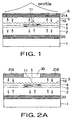
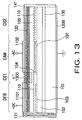
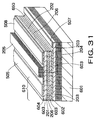
- Fig. 1 is a cross-sectional conceptional diagram schematically showing construction of a central part of a DFB laser according to the first embodiment of the invention.
- the laser shown here is a InGaAsP/InP edge-emitting DFB laser having 2nd-order diffraction gratings 10, and Fig. 1 shows it in a cross-sectional conceptional diagram taken along a plane parallel to the waveguide direction of its cavity.
- a high-reflectivity structure 20 made up of InGaAsP layers and InP layers is made on an n-type InP substrate 1. Further formed thereon are an n-type InP buffer layer 2 with the thickness of 1 micrometers strained MQW active layer 3 made of InGaAsP (PL (photoluminescence) wavelength: 1.3 micrometers), and InGaAsP waveguide layer 4 (PL wavelength: 1.12 micrometers) continuously by crystal growth. Formed on the waveguide layer 4 are 2nd-order diffraction gratings 10. The diffraction gratings 10 have formed a discontinuous portion 11 (phase shift) with the period of ⁇ (wavelength)/4.
- a p-type InP cladding layer 5 high-reflectivity structure 21 and p-type InGaAsP contact layer 6 (PL wavelength: 1.15 micrometers).
- the high-reflectivity structure 21, similarly to the high-reflectivity structure 20, may be made by alternately stacking InGaAsP layer and InP layers to form a multi-layered Bragg reflector.
- electrodes On the upper and lower surfaces of the element, electrodes, not shown, are made, respectively.
- the DFB laser according to the invention as shown in Fig. 1 is explained, comparing it with a DFB laser as a comparative example obtained during researches toward the present invention.
- DFB lasers in general, are characterized in providing diffraction gratings along the waveguide and utilizing Bragg diffraction light from the diffraction gratings for optical feedback to invite laser oscillation. Since a vertical mode is selected among various modes of radiation, DFB lasers are advantageous in that oscillation in a single longitudinal mode is possible. Because of this advantage, DFB lasers are currently used as light sources of high-speed optical transmission or measurement using optical fibers.
- Diffraction gratings used in DFB lasers involve 1st-order gratings and 2nd-order gratings.
- first-order gratings have a 1st-order period corresponding to a radiation wavelength.
- 2nd order gratings have a period twice that of a 1st-order gratings, and are readily made.
- the period of the 1st-order gratings is approximately 0.2 micrometer. Processing accuracy required for making them is almost 0.1 micrometer, control of their depth is also difficult.
- the period of 2nd-order gratings is 0.4 micrometer, and it is much easier to make them.
- DFB lasers having 2nd-order gratings emit radiation mode light in both opposite directions vertical to the waveguide, namely, to the substrate side and the superstrate side.
- DFB lasers having 1st-order gratings there is no such radiation mode. That is, when 2nd-order gratings are used, the radiation mode becomes a loss, and causes an increase of the threshold value. Therefore, in spite of the difficulty of their fabrication, 1st-order diffraction gratings were usually employed to ensure appropriate characteristics such as threshold value.
- GCSEL grating-coupled surface emitting laser
- 2nd-order gratings This is a surface emitting laser which uses as its output radiation mode light emitted vertically to the substrate. It does not require facets made by cleavage, and can be tested as wafer in the manufacturing process of the device.
- Fig. 6 schematically shows a cross-sectional configuration of a DFB laser element as such a comparative example. That is, Fig. 6 shows a comparative example of InGaAsP/InP surface emitting laser.
- a high-reflectivity multi-layered structure 20 made up of InGaAsP layers and InP layers is made on an n-type InP substrate 1, and further formed thereon are an n-type InP buffer layer 2 with the thickness of 1 micrometer, strained MQW active layer 3 made of InGaAsP (PL (photoluminescence) wavelength: 1.3 micrometers), and InGaAsP waveguide layer 4 (PL wavelength: 1.12 micrometers) continuously by crystal growth.
- PL photoluminescence
- radiation mode light is radiated vertically to the substrate. If the radiation mode light is taken out vertically to the substrate surface, then the laser is a surface-emitting laser. The radiation mode light is emitted in both the upper and lower directions vertical to the substrate.
- the DFB laser according to the invention as shown in Fig. 1 not only prevents a rise of the threshold value by the loss of the radiation mode but also prevents spatial holeburning.
- the embodiment shown in Fig. 1 since the high-reflectivity structure 21A is provided also above the waveguide, the radiation mode derived from 2nd-order gratings does not go out externally. Therefore, the radiation mode loss can be reduced, and a rise of the threshold value can be prevented.
- the embodiment, using 2nd-order gratings, also has the advantage that its fabrication is easy.
- the use of the phase shift 11 enables appropriate control of spatial distribution of light and carriers.
- the illustrated example if reflection from both edges of the laser is small and coupling force between the gratings and the guided mode is somewhat large, then an intensity profile in which both the guided mode and the radiation mode get intensive at the phase shift 11 at the center.
- This intensity distribution profile is schematically shown in Fig. 1.
- the freedom of controlling the guided mode intensity in the axial or transverse direction is increased without changing the structure of the active layer itself or changing the electrode structure. Therefore, asymmetry of edge outputs and a novel gain-guided structure can be realized.
- the threshold value of approximately 9 mA was obtained in a DFB laser having a buried-hetero-structure, 1 micrometers wide, according to the structure shown in Fig.1. Since the threshold value was approximately 8 mA also in a comparative example using 1st-order gratings, it was confirmed that an element exhibiting practically favorable threshold characteristics even with second-order gratings be obtained. Additionally, the laser using second-order gratings could be fabricated much easier.
- Fig. 2A is across-sectional conceptional diagram taken along the waveguide direction to schematically show construction of a central part of GCSEL using second-order gratings.
- This GCSEL shown here is generally the same in construction as the semiconductor laser explained with reference to Fig. 1. So, identical portions are labeled with common reference numerals, and detailed explanation thereof is omitted.
- One of important features of GCSEL of Fig. 2A lies in an output window 30 being opened to extract as its output the radiation mode light from a central region of approximately 50 micrometers with a large radiation mode intensity in the optical axis direction of a cavity which is approximately 250 micrometers long. That is, in this portion, no high-reflectivity structure is provided, a material transparent to the radiation mode light is used.
- a high-reflectivity structure 21b is provided also on the superstrate side in the region except the output window 30.
- the high-reflectivity structure 21B and the substrate-side high-reflectivity structure 20 make the radiation mode to the waveguide. Therefore, the radiation loss is minimized, and increase of the threshold value can be prevented.
- the phase shift 11 provided near the center of the cavity controls spatial distribution of light and carriers.
- the phase shift 11 controls spatial distribution of light and carriers.
- the gain/loss profile along the optical axis of the cavity in this manner, radiation from the output window 30 can be increased, and simultaneously, non-uniformity of the carrier density can be compensated so as to prevent spatial holeburning.
- Fig. 2B shows a flowchart showing a fabrication process of the GCSEL of Fig. 2A.
- the laser according to the embodiment can be made by a relatively easy process.
- a high-reflectivity structure 20 made up of InGaAsP layers and InP layers is made on an n-type InP substrate 1. Further formed thereon are an n-type InP buffer layer 2 with the thickness of 1 micrometer, strained MQW active layer 3 made of InGaAsP (PL (photoluminescence) wavelength: 1.3 micrometers), and InGaAsP waveguide layer 4 (PL wavelength: 1.12 micrometers) continuously by crystal growth. Formed on the waveguide layer 4 are 2nd-order diffraction gratings 10. The diffraction gratings 10 have formed a discontinuous portion 11 (phase shift) with the period of ⁇ (wavelength)/4.
- high-reflectivity structure 21B Further grown thereon are a p-type InP cladding layer 5, high-reflectivity structure 21B.
- the high-reflectivity structure 21B similarly to the high-reflectivity structure 20, may be made by alternately stacking InGaAsP layer and InP layers to form a multi-layered Bragg reflector.
- zinc (Zn) is diffused selectively into the high-reflectivity structure 21B and annealed.
- the Zn-incorporated region is disordered and broken into a region of a uniform intermediate composition. That is, by diffusing Zn into the region for the window of the high-reflectivity structure formed on the entirety of the element to disorder it, the window 30 with a low reflectance can be made.
- a p-type InGaAsP contact layer (not shown) may be formed on the reflector 21B, and electrodes (not shown) are formed on the upper and lower surfaces of the element respectively.
- Fig. 3 is a cross-sectional conceptional diagram taken along the waveguide direction to show construction of a central part of an edge-emitting DFB laser using second-order gratings
- this laser is similar in construction to the semiconductor laser explained with reference to Fig. 1. So, identical portions are labeled with common reference numerals, and detailed explanation thereof is omitted.
- the high-reflectivity structure 20 is provided throughout the entire area under the cavity. Above the cavity, however, a high-reflectivity structure 21C is provided only adjacent to one facet F, and the remainder portion remains as a low-reflectivity region 30'. Near the center of the cavity, the phase shift 11 is provided in the gratings 10.
- optical outputs from front and rear facets are approximately equal. Practically, however, it is desirable that optical output from the front facet F be larger and optical output from the rear facet for use in monitoring be smaller.
- the embodiment shown here provides the high-reflectivity structure 21C merely above the portion adjacent to the front facet F. Then, since the radiation mode loss of second-order gratings decreases in the portion adjacent to the front facet F, its optical intensity becomes larger than that of the portion adjacent to the rear facet with a larger loss. As a result, large optical output from the front facet F is ensured.
- disordering by diffusion of zinc (Zn) can be used. That is, by making the high-reflectivity structure of a multi-layered structure over the entire surface above the cavity and next diffusing zinc only into the portion adjacent to one facet to disorder the high-reflectivity structure, the low-reflectivity region 30' can be made.
- Fig. 4 is a cross-sectional conceptional diagram taken along a transverse direction to show construction of a central part of an edge emitting DFB laser using second-order gratings. That is, Fig. 4 is a cross-sectional view taken along a plane vertical to the waveguide of the cavity, which is rotated from preceding drawings by 90E and viewed from the direction of a facet.
- the laser shown here has a gain-guided structure instead of an index-guided structure.
- the active layer 3 is a slab.
- the active layer is excited by a current flowing from a stripe-shaped electrode 40, and light is guided accordingly.
- the transverse mode is not stabilized. That is, as the optical intensity increases, the carrier density in the central portion of the waveguide with a high photon density becomes lower and decreases the gain, undesirable high-order transverse modes are liable to occur.
- the embodiment shown here provides a high-reflectivity structure 21D narrower than the width of the stripe-shaped electrode 40 to lie above the electrode in alignment with the center of the stripe. At opposite sides of the stripe-shaped high-reflectivity structure 21D, the low-reflectivity region 30' lies.
- the effect by the return of the radiation mode by reflection from the high-reflectivity structure 21D progressively increases towards the center of the stripe where the photon density is high, and the decrease in gain in along the center of the stripe can be compensated relatively.
- the transverse mode can be stabilized.
- disordering by diffusion of zinc (Zn) can be used. That is, by making the high-reflectivity structure of a multi-layered structure over the entire surface above the cavity and next diffusing zinc into opposite sides of the stripe to disorder the high-reflectivity structure, the low-reflectivity region 30' can be made.
- Fig. 5 is a cross-sectional conceptional diagram taken along the waveguide direction to schematically show construction of a central part of GCSEL using second-order gratings.
- GCSEL shown here is similar in construction to the semiconductor laser explained with reference to Fig. 1. So, identical portions are labeled with common reference numerals, and detailed explanation thereof is omitted.
- One of important features of GCSEL of Fig. 5 lies in a high-reflectivity structure 21E being provided above a central part of the cavity where the radiation mode is intensive. That is, the laser according to the instant embodiment is configured to extract as its optical output the radiation mode light passing through the high-reflectivity structure 21E.
- the high-reflectivity structure 21E is provided in a central part of the cavity where the radiation mode is intensive, its optical output decreases, but the oscillation threshold value can be lowered by reducing the radiation loss. As a result, temperature characteristics of laser oscillation can be improved. Simultaneously, by adjusting distribution of light and carriers along the optical axis of the cavity, spatial holeburning can be prevented to thereby stabilize the oscillation mode.
- the optical output is relatively low, a surface emitting laser with a low oscillation threshold value and good oscillation characteristics can be realized. So, it is suitable for use in various applications in which the oscillation property is more important than optical output.
- disordering by diffusion of zinc (Zn) can be used. That is, by making the high-reflectivity structure of a multi-layered structure over the entire surface above the cavity and next diffusing zinc into opposite sides excluding the central part of the cavity to disorder the high-reflectivity structure, the low-reflectivity region 30' can be made.
- DFB lasers embodying the invention have been explained above with reference to Figs. 1 through 6.
- the invention is not limited to these specific examples, but is applicable to various other devices within the concept of the invention.
- the invention is similarly applicable also to other DFB lasers using various materials, such as GaAlAs/GaAs lasers and GaInAlP/GaAs lasers, and attains similar various effects.
- the specific examples have been explained as providing the high-reflectivity structure in a selective location above the waveguide and simultaneously providing a window region.
- the invention is not limited to such configurations.
- the high-reflectivity structure is provided in a selective portion below the waveguide, i.e., on one side nearer to the substrate, and the window region is provided therein, the same effects can be obtained.
- the reflectance of a high-reflectivity region may be locally decreased to selectively form the high-reflectivity structure and the low-reflectivity structure.
- the high-reflectivity region may be made by using metal films or in form of a multi-layered structure of dielectric thin films.
- the spatial arrangement of the high-reflectivity structure one made up of a number of micro structures or a periodic structure may be used similarly.
- DFB lasers embodying the invention have the nature weak at return light. That is, external return light may disturb oscillation conditions of a single longitudinal mode once established. This may invite fluctuations in oscillation wavelength (called wavelength chirp) and, in the worst case, may invite instability of the longitudinal mode, such as jump, or the like.
- wavelength chirp fluctuations in oscillation wavelength
- DFB lasers need an optical isolator.
- the Inventor also invented a novel, high-performance optical isolator.
- optical isolators suitable for use together with DFB lasers and optical integrated elements integrating them, as sixth to eleventh embodiments of the invention, with reference to Figs. 7A through 14.
- Fig. 7A is a conceptional diagram schematically showing construction of a first optical isolator according to the invention. That is, Fig. 7A illustrates a cross-sectional configuration of the optical isolator, taken along the longitudinal direction of the waveguide.
- the optical isolator shown here is made up of an InGaAs absorption layer 130, n-type InP cladding layer 102, InGaAsP layer 104, p-type InP cladding layer 105, p-type InGaAsP layer 106 and reflection structure 120 which are stacked sequentially on an n-type InP substrate 101.
- the absorption layer 130 may be made of any material having a high absorption coefficient relative to radiation mode light. For example, it may be made by using a semiconductor material having a smaller band gap than that of the waveguide layer 104.
- second-order diffraction gratings 110 having a sawtoothed asymmetric cross-sectional configuration as shown in Fig. 7A.
- the "number of order " of the diffraction gratings is determined by the period of the diffraction gratings and the wavelength of light causing diffraction by Bragg reflection.
- first-order gratings have a first-order period corresponding to the wavelength of the light.
- Second-order gratings have a period twice that of first-order gratings.
- the period of first-order gratings is approximately 0.2 micrometers. Processing accuracy required for making them is almost 0.1 micrometers, control of their depth is also difficult.
- the period of 2nd-order gratings is 0.4 micrometers, and it is much easier to make them.
- the reflection structure 120 may be a multi-layered Bragg reflective film made by alternately stacking two kinds of dielectric films different in refractive index. By appropriately determining refractive indices and thickness of individual layers in the multi-layered Bragg reflective film, a reflection structure exhibiting a high reflectance to radiation mode light can be obtained.
- a manufacturing process of the optical isolator shown in Fig. 7A is outlined below.
- First grown on the n-type InP substrate 101 is the InGaAs absorption layer 130 for radiation mode light up to the thickness of 2.5 micrometers.
- the n-type InP cladding layer 2 is grown to the thickness of approximately 1 micrometers which is a thickness not affecting the guided mode. That is, the absorption layer 130 is located distant enough not to affect exudation of guided mode light into the cladding layer.
- the InGaAsP layer 104 is grown approximately 0.3 micrometers thick. Crystal growth heretofore is progressed continuously.
- sawtoothed asymmetric second-order gratings 110 having a blaze angle in the illustrated direction are made to form a waveguide.
- the gratings can be made, for example, by applying a resist onto the surface of the waveguide layer 104, exposing it by EB (electron beam) exposure, then treating the surface by ion milling while inclining the substrate, and finally finishing the surface with an appropriate etchant.
- the dept of gratings obtained in this manner is approximately 0.1 micrometers.
- the p-type InP cladding layer 105 approximately 1 micrometer thick. Further grown is the p-type InGaAsP layer 106 for surface protection.
- These layers are p-type layers here, taking it into account that the optical isolator may be integrated with a DFB laser. However, they may be n-type layers if exclusively used as an independent optical isolator.
- the reflection structure 120 which may be a dielectric multi-layered film, is stacked. Reflectance of the reflection structure 120 may be, for example, approximately 95%.
- the reflection structure 120 similarly to the absorption layer 130, is located almost outside the region where the guided mode may exude, so as to prevent affection to the guided mode light. In this manner, the optical isolator shown in Fig. 7A is completed.
- the optical isolator shown in Fig. 7A has second-order or higher-order diffraction gratings.
- a waveguide structure, especially having second-order gratings emits radiation mode light vertically to the waveguide direction to both the substrate side and the superstrate side.
- Second-order gratings of the optical isolator of Fig. 7A has a cross-sectional configuration asymmetric in the propagating direction, that is, having a blaze angle.
- the blaze angle intensifies the radiation mode on the substrate side or the radiation mode on the superstrate side, relative to the propagating direction of optical waves in one of the left and right directions. If the traveling direction or optical waves is reversed, then the distribution ratio between the substrate side and the superstrate side is also reversed.
- Fig. 7A in the case where the guided light travels from right to left, almost all of the radiation mode light is emitted toward the substrate 101 as shown by arrow C. This light is absorbed by the absorption layer 130, not returning to the waveguide, and makes the guiding loss.
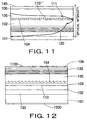
- Fig. 8 is a graph showing waveguide characteristics of asymmetric diffraction gratings. his is a graph printed in IEEE Journal of Quantum Electronics, vol. QE-12, pp. 4494-4499, 1976, under the title "Analysis of Grating-Coupled Radiation in GaAs:GaAlAs Lasers and Waveguides - II: Blazing Effects" by Strefer, et al.
- the horizontal axis of Fig. 8 represents shape parameters ⁇ of diffraction gratings, and the vertical axis represents optical outputs emitted from diffraction gratings.
- the shape parameter ⁇ on the horizontal axis shows asymmetry (blaze angle) of the cross-sectional configuration of a diffraction grating.
- a reflection structure is provided only on one side of such asymmetric diffraction gratings. Since the reflection structure makes the radiation mode return to the waveguide structure, the loss in the waveguide structure is reduced. That is, the loss of the guided light travelling in this direction decreases.
- the invention can realize the structure which guides only the guided light in one direction (in this case, direction from left to right) under a small loss, and can realize a very compact waveguide optical isolator having a high direction selectivity.
- Fig. 14 is a conceptional perspective view schematically illustrating construction of one of these conventional optical isolators.
- the optical isolator shown here is configured to locate diffraction gratings 1111 aslant of the waveguide direction on a semiconductor substrate S, in order to decrease the refractive index n2 on one side of the waveguide structure to establish asymmetry while dispersing return light as the radiation mode to the n2 side.
- the waveguide structure is asymmetric on left and right sides, output beams exhibit left-and-right asymmetric distribution, and the coupling force with optical fibers deteriorates.
- the layer with the different refractive index n2 must be made separately by crystal growth, the manufacturing process is complicated. Furthermore, it involved another problem that, when inclined diffraction gratings are used, its coupling as a DFB laser deteriorates.
- the invention removes such requirement. That is, the invention permits completely the same stripe structure as used conventionally. Therefore, the invention does not increase any subsequent step. Additionally, it has the advantage that NFP (near field pattern) of the guided mode is symmetric, and can be readily coupled optically to fibers.
- NFP near field pattern
- Fig. 7B is a conceptional cross-sectional view illustrating a modified version of the optical isolator shown in Fig. 7A.
- gain media 150 are provided between the diffraction gratings 110 and the reflection structure 120.
- Radiation mode light radiated upward to the side opposite from the substrate as shown by arrow A is amplified by the gain media 150, reflected by the reflection structure 120, again amplified by the gain media 150 and returns to the waveguide 104. That is, guided light travelling from left to right in Fig. 7B is amplified very effectively, and the directivity of the isolator is so much further improved.
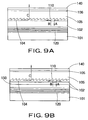
- Fig. 9A is a cross-sectional conceptional diagram illustrating construction of a central part of the second optical isolator according to the invention.
- second-order or higher-order diffraction gratings 110 are provided, and a reflection structure and an absorption structure are provided above and below the gratings 110.
- the second optical isolator is different from the first optical isolator in the following two points.
- the reflection structure 120 may be a high-reflectivity DBR(distributed Bragg reflector) in form of a multi-layered structure of semiconductor crystal layers, for example.
- Usable as the anti-reflection coat 140 is, for example, a 1/4 wavelength film, i.e. a dielectric thin film having the thickness of ⁇ /4n where ⁇ is the wavelength of radiation mode light and n is the refractive index.
- the other components may be the same as those of the first optical isolator explained above with reference to Fig. 7A. So, common reference numeral are attached to them, and their detailed explanation is omitted.
- Fig. 9B is a schematic cross-sectional view showing a modified version of the optical isolator of Fig. 9A. That is, the isolator shown here has formed gain media 150 between the waveguide 104 and the reflection structure 120. Radiation mode light radiated toward the substrate as shown by arrow A is amplified by the gain media 150, reflected by the reflection structure 120, again amplified by the gain media 150 and returns to the waveguide 104. That is, guided light travelling from left to right in Fig. 9B is amplified very effectively, and the directivity of the isolator is so much further improved.
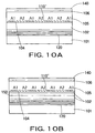
- Fig. 10A is a cross-sectional conceptional diagram illustrating construction of a central part of the third optical isolator according to the invention.
- diffraction gratings 110' are provided, and the absorption structure 140 and the reflection structure 120 are provided above and below the gratings 110', respectively.
- the basic structure and its function are substantially the same as those of the second optical isolator explained with reference to Fig. 9A. So, components thereof are labeled with common reference numerals, and their detailed explanation is omitted.
- the gratings 110' have two kinds of periods, ⁇ 1 and ⁇ 2. In this manner, it can operate as an optical isolator for two kinds of guide light having different wavelengths corresponding to these periods.
- the dynamic range of available wavelengths of the optical isolator can be enlarged.
- the profile of guided light and radiation mode light in the cavity axial direction can be controlled by the phase shifting effect.
- the optical isolator is configured to cope with any of guided light of three or more different wavelengths. If the gratings change in period continuously, the optical isolator is available for any guided light in a range of continuous wavelengths.
- Fig. 10B is a schematic cross-sectional view showing a modified version of the optical isolator shown in Fig. 10A.
- gain media 150 are provided between the waveguide 104 and the reflection structure 120. Radiation mode light radiated toward the substrate as shown by arrow A is amplified by the gain media 150, reflected by the reflection structure 120, again amplified by the gain media 150 and returns to the waveguide 104. That is, guided light travelling from left to right in Fig. 10B is amplified very effectively, and the directivity of the isolator is so much further improved.
- Fig. 11 is a cross-sectional conceptional diagram illustrating construction of a central part of the third optical isolator according to the invention.
- the optical isolator shown here has a construction similar to that of the second optical isolator explained with reference to Fig. 9A. So, the same or equivalent components thereof are labeled with common reference numerals, and their detailed explanation is omitted.
- a different of the instant embodiment lies in that a portion discontinuously shifted in period, that is, a phase shift 111, is provided in the diffraction gratings 110''.
- the shift amount of the phase shift 111 may be, for example, ⁇ /4 where ⁇ is the guide wavelength.
- the phase shift 111 enables control of the profile of guided light and radiation mode light along the cavity axial direction.
- the isolator waveguide shown in Fig. 11 has a good transmittance to right-going guided light and exhibits large attenuation to oppositely traveling light.
- the attenuation ratio increases due to a difference in phase between optical waves and the diffraction gratings 110.
- the phase shift 111 is provided nearer to the exit (right) of the isolator waveguide of Fig. 11, although attenuation of right-going guided light is small, left-going guided light is largely attenuated because the distance after passing the phase shift 111 is long. This is shown in form of changes in optical intensity by arrow-containing lines. That is, the phase shift 111 promises more effective isolation.
- phase shift introduced in the instant embodiment can be introduced similarly into the first and third optical isolators to obtain similar effects.
- Fig. 12 is a cross-sectional conceptional diagram showing construction of a central part of the sixth DFB laser embodying the invention. That is, the DFB laser according to the embodiment is a specific example which applies the structures and principles of operation of the optical isolators according to preceding embodiments.
- the laser shown in Fig. 12 has the same structure as the first optical isolator shown in Fig. 7A, for example. Therefore, the same components as those of Fig. 7A are labeled with common reference numerals, and their detailed explanation is omitted.
- the DFB laser of Fig. 12 has the active layer 103.
- the active layer 103 has the role of emitting light and guiding the optical waves.
- the active layer 103 may be either a single semiconductor layer or a multi-layered high-efficiency structure such as MQW (multiquantum well) structure.
- the reflection structure 120 is made of a p-type semiconductor layer.
- the p-type InGaAsP layer 106 plays the role of improving contact with electrodes.
- a p-side electrode 1100 and an n-side electrode 1200 are provided for electric conduction.
- DFB lasers components of guided light traveling in left and right directions are mutually fed back via diffraction gratings and resonate to cause oscillation.
- the radiation mode loss of right-going guided light is small, and optical output from the right facet increases.
- the radiation mode loss of left-going guided light is large, the output intensity at the left facet does not increase so much.
- the embodiment shown here can improve the slope efficiency in terms of outputs. Additionally, since the laser itself includes the isolator function, resistance to return light is also reinforced. Considering that DFB lasers, in general, are liable to become unstable in oscillation conditions especially by return light, the instant embodiment is particularly effective in this respect.
- the embodiment shown here is also effective in improving the single longitudinal mode performance because the gain difference of threshold value between longitudinal modes becomes large.
- the invention can similarly provide DFB lasers with structures compatible with optical isolators according to the second to fourth embodiments, in addition to the specific examples shown above. That is, DFB lasers having effects corresponding to the above-mentioned various effects can be obtained by reversing the positional relation between the absorption structure and the reflection structure, changing the period of the diffraction gratings, or introducing a phase shift into the gratings.
- DFB lasers are surface-emitting lasers. That is, when using as the output the light emitted externally through the reflection structure 20 or the absorption structure in one side of the gratings, a surface-emitting DFB laser can be realized, which is not so high in optical output but remarkably excellent in threshold value and other oscillation characteristics.
- the surface-emitting DFB laser of this type can be readily integrated with any of optical isolators according to the above-explained embodiments, and a very compact, high-performance optical integrated element combining optical an isolator and a surface-emitting laser can be realized.
- Fig. 13 is a cross-sectional conceptional diagram showing construction of a central part of the optical integrated element embodying the invention.
- the optical integrated element according to the embodiment is made by integrating a plurality of elements on a monolithic, i.e. common, substrate.
- a specific example is shown, in which the DFB laser of Fig. 12, optical isolator of Fig. 7A and waveguide EAM (electro-absorption modulator) are integrated monolithically.
- the DFB laser is DC-driven via the p-side electrode 1101.
- the region where the absorption layer 107 lies is EAM.
- EAM can be modulated in absorption coefficient by applying a negative voltage to the p-side electrode 1102.
- Guided light generated in the active layer 103 of the DFB laser is modulated in correspondence with changes in absorption coefficient, and output to the right side in Fig. 13.
- An optical isolator OI1 is provided between the DFB laser and EAM.
- the optical isolator OI1 has a proton (H + ) bombarded region 1300 to electrically isolate DFB from EAM.
- H + proton
- return light is input to the DFB laser and causes undesirable fluctuation of optical output and wavelength.
- another optical isolator OI2 can be integrated also on the output side of EAM in a similar simple process, and return light from the exterior can be prevented.
- the DFB laser, optical isolator OI1, EAM and second optical isolator OI2 can be integrated very compactly. Additionally, since these elements shares the waveguide, their optical coupling is ensured sufficiently.
- the absorption layer 130, gratings 110 and reflection structure 120 of the optical integrated element can be made in a common manufacturing process, a high-performance optical integrated element can be made in a simple process.
- positional relation of gratings, reflection structure, absorption/anti-reflection structure, as well, is not limited to upper and lower directions of the substrate.
- diffraction gratings may be formed on a side surface of the waveguide, that is, a surface vertical to the substrate, and the reflection structure and the absorption structure may be located at opposite sides thereof. In this case, the reflection structure, diffraction gratings and absorption structure result in lying in parallel with the substrate surface.
- radiation mode light emitted from a waveguide having a hologram capable of generating radiation mode light is amplified by a separate amplifier means, and returned to the waveguide by using a reflection means. Since radiation mode light is emitted to both sides of the waveguide, reflection means is preferably provided at opposite sides.
- the invention involves a lot of applied inventions based on the unique cavity structure. One of them is an amplifier.
- the invention also involves optical modulators, laser oscillators, couplers and optical transmission devices using them.
- Fig. 15 is a conceptional diagram showing the first optical functional element according to the invention.
- Optical functional elements according to the invention have a waveguide means for guiding light.
- an optical waveguide 201 is provided as the waveguide means.
- Formed on the optical waveguide 201 are second-order diffraction gratings 202.
- the waveguide 201 may be either an optical fiber, vertically used dielectric waveguide or semiconductor waveguide.
- an InGaAsP/InP waveguide may be used.
- This is a multi-layered structure (slab waveguide) including an InGaAsP quaternary mixed crystal with a high refractive index as a core which is sandwiched by InP with a low refractive index from upper and lower sides.
- Fig. 15 shows a longitudinal cross-section, but a two-dimensional buried waveguide sandwiching the core by InP also from the lateral directions may be used.
- Part of light guided by the waveguide 201 having the second-order grating 202 is emitted to both upper and lower directions substantially vertically of the waveguide direction. This is the radiation mode light.
- the present invention employs a structure where the radiation mode light is guided through the amplifier means 203.
- the amplifier means 203 functions to amplify light. It may be either EDFA (erbium-doped fiber amplifier), SOA (semiconductor optical amplifier), optically pumped gain media, or any other appropriate element. For example, it may be a p-n junction of an electrically conducted InGaAsP/InP multi-layered structure.
- the amplifier means 203 is preferably located sufficiently distant not to directly disturb the function of guiding the guided mode by the waveguide 201. This is in accordance with the concept of the invention that a cavity structure is made for optical waves converted from the guided mode to the radiation mode.
- the reflection means with a high reflectance is located.
- the reflection means 204 functions to reflect radiation mode light with a high reflectance, and it may be a dielectric multi-layered film, for example. Radiation mode light reflected by the reflection means 204 is again amplified in the amplifier means 203, and returns to the waveguide 201 via the gratings 202. By repeating the cycle of amplification, reflection and amplification, a unique cavity structure can be realized. More specific structures of optical functional elements will be described later.
- Fig. 16 is a conceptional diagram showing the second optical functional element according to the invention. That is, in the element shown here, a more intensive cavity means is realized by providing the above-explained cavity structure both above and below the waveguide 201. That is, components of radiation mode light emitted upward and downward of the waveguide 201 undergo the cycle of amplification, reflection and amplification.
- radiation mode light has a flexibility permitting construction of various optical functions along the waveguide, unlike outputs of waveguide facets regarded as a point light source. For example, there is the function of collecting input and output light for coupling with other optical elements. More specifically, there are lens functions, different holograms, and optical isolators, for example.
- Fig. 17 is a conceptional diagram showing the third optical functional element according to the invention.
- the embodiment shown here is a version including a phase control means 205 in addition to the construction of the second optical functional element explained above.
- the phase control means 205 has the function of controlling the phase of light to adjust the phase of reflected light so that the reflected light from the reflection means 204 can efficiently couple to the waveguide 201 via the gratings 202.
- phase control means 205 is an InGaAsP/InP slab waveguide structure having a p-n junction. By electrically feeding the p-n junction of the waveguide or applying a reverse bias electric field, the refractive index changes, and the phase of light can be controlled.
- the phase control means 205 may be interposed between the amplifier means 203 and the reflection means 204, or between the waveguide 201 and the amplifier means 203.
- the amplifier means 203 can be changed carrier density and hence in refractive index by electrical supply. In an application, it may be cancelled by the phase control means 205.
- T(x) is a function determined by Fourier coefficients of the gratings and the field of the guided mode.
- C a and C b are constants determined by boundary conditions.
- C a r g Be j 2 kg - A 1- r 0 r g Be j 2 kg
- Equation (3) becomes zero, and constants C a and C b become infinities. That is, as understood from Equations (1) and (2), the cavity oscillates as a "radiation mode cavity". In other words, it is understood that oscillation occurs when the reflectance is large, a gain is ensured, and the phase condition is satisfied.
- Figs. 15 through 17 Construction shown in Figs. 15 through 17 is the basis of various elements explained below. In the present invention, however, components like the amplifier means and reflection means need not exist independently from each other. For example, like the optical functional element next explained with reference to Fig. 18, two or more means may be commonly involved in a single component.
- Fig. 18 is a conceptional diagram showing construction of the fourth optical functional element according to the invention.
- the optical functional element of Fig. 18 includes no media 203 having a gain. Instead, it includes an active layer 206 having a gain near the waveguide 201.
- the reflection means 204' also has a gain. That is, the active layer 206 and reflection means 204' behave as amplifier means.
- a p-n junction may be made in DBR (distributed Bragg reflector) in form of a multi-layered film of semiconductors stacked in parallel in the substrate surface to make it have a gain by current injection, or another waveguide may be made vertically to the waveguide 201 to make DBR therein.
- DBR distributed Bragg reflector
- Fig. 19 is a conceptional diagram showing the fifth optical functional element according to the invention.
- second- or higher-order diffraction gratings 202 have a phase shift 220, i.e. a phase discontinuity.
- the phase shift 220 is effective for control of intensity profile of radiation modes parallel to the waveguide. That is, if a radiation mode generates from the waveguide, the waveguide accepts two waves opposite in travelling direction.
- the intensity profile of radiation modes in the axial direction i.e.
- phase shift affects the axial intensity of guided modes themselves, it can be an important component of the present invention.
- the axial intensity profile of radiation modes fed back with a gain and the intensity of the guided mode coincide. Since they spatially strongly synchronize in the phase shifting position, there is obtained the effect that the optical feedback, i.e. the efficiency of the cavity, increases remarkably.
- phase shift preferably has a phase shift amount in the range from several integer times the guide wavelength ⁇ /r to a value not smaller than 1/8 and not larger than 3/8.
- the above-raised value 1/4 is the center value of this range.
- Fig. 20 is a conceptional diagram showing the sixth optical functional element according to the invention.
- components or parts identical or equivalent to those of the embodiments explained with reference to Figs. 15 through 19 are labeled with common reference numerals, and their detailed explanation is omitted.
- the embodiment shown here has a so-called blaze angle with which the cross-sectional configuration of the diffraction grating 202 is asymmetric. With diffraction gratings with a symmetric cross-sectional configuration having no blaze angle, radiation modes generated by guided modes travelling in a predetermined direction tend to be emitted uniformly in both upper and lower two directions.
- a blaze angle makes radiation modes emitted upward and downward to have a selectivity.
- optical waves travelling through the waveguide from left to right are emitted upward of the drawing sheet with a larger ratio, and those in the opposite direction are emitted downward with a smaller ratio.
- the optical functional element shown here can be explained by using the constructions shown in figs. 15 through 20. That is, in this embodiment, the waveguide means, amplifier means and reflection means are modulated independently from each other. These are basic requirements of optical active devices dealing with optical signals, together with the phase control means explained above with reference to Fig. 17.
- Equation (5) conditions defined by the above-introduced Equation (5) are satisfied by modulating the amplifier means, and oscillation of the cavity vertical to the waveguide can be controlled by current injection.
- Other means, such as waveguide means and reflection means, can be similarly modulated in parameter.
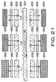
- Fig. 21 is a conceptional diagram showing the optical functional element according to the embodiment.
- components or parts identical or equivalent to those of the embodiments explained with reference to figs. 15 through 20 are labeled with common reference numerals, and their detailed explanation is omitted.
- another cavity structure using radiation modes is made along the cavity. Making it along the waveguide means the use of the entire length of the long waveguide.
- the cavity structure can be made to be variable along the waveguide. It is also possible to make a number of cavity structures along the waveguide.
- the diffraction gratings 202 of the waveguide structure 201 changes in period along the waveguide.
- the gratings have three kinds of periods, ⁇ 1, ⁇ 2, and ⁇ 3.
- the reflection means 204, phase modulator means 205, amplifier means 203 are provided.
- the waveguide 201 is held excited to make it generate spontaneous radiation light.
- Radiation modes of wavelength components radiated vertically in response to grating periods ⁇ 1, ⁇ 2, and ⁇ 3 among the spontaneous radiation light are amplifier in respective radiation mode cavities.
- Degree of amplification can be determined by independently controlling the gain, reflectance, phase, and so forth, to desirably amplify selected wavelengths.
- the reflection means itself, can be reinforced in wavelength selectivity by employing a structure like DBR. It is also possible to adjust the peak of the gain spectrum to a specific wavelength. If amplification is strong, oscillation is also possible. It is also possible to extract the amplified light from respective cavities. It can also be returned to the waveguide 201 and extracted from its facet. Additionally, it is possible to extract specific wavelengths as modulated signals from respective cavities.
- the waveguide means and other means can be integrated monolithically on an substrate of InP, for example.
- the waveguide for example, may be id fiber, and the gratings may be fiber gratings.
- Fig. 22 is a conceptional diagram showing the ninth optical functional element according to the invention.
- components or parts identical or equivalent to those of the embodiments explained with reference to Figs. 15 through 21 are labeled with common reference numerals, and their detailed explanation is omitted.
- the construction of Fig. 22 is similar to that of the eighth optical functional element explained above.
- the waveguide 201 is a transmission line in which signals, particularly a plurality of signals different in wavelength, propagate.
- the embodiment shown here corresponds to a tuner amplifier.
- the transmission system in the embodiment shown here is also a ring network, That is, a signal introduced from the left end of the waveguide is output also from the right end, and detected also in another terminal.
- the amplifying function of radiation modes by the cavity structure also functions as a repeater and prevents attenuation of the signal.
- Behaviors of the element according to the embodiment is based on the concept of the eight embodiment explained above. That is, radiation modes radiated vertically from diffraction gratings different in period are amplified by wavelength-selective cavities, and their outputs are detected.
- respective cavities are regarded as output ports, signals having different wavelengths are output downward on the drawing sheet from respective ports, and are received by detectors 240.
- the wavelength distance among ⁇ 1, ⁇ 2, and ⁇ 3 are large, they are radiated in directions offset from the vertical direction relative to the waveguide in portions of the gratings other than those with periods corresponding to these wavelengths. Therefore, tuning is realized merely by adjusting locations of the cavities. Tuning is possible also by modulating the refractive index of the waveguide.
- tuning can be made by modulating the phase control means 205 or by changing the refractive index of the DBR reflection means.
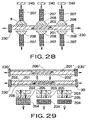
- Fig. 23 is a conceptional diagram showing the optical functional element according to the embodiment.
- components or parts identical or equivalent to those of the embodiments explained with reference to Figs. 15 through 22 are labeled with common reference numerals, and their detailed explanation is omitted.
- the embodiment shown here is centralized to an optical functional element having the function of laser oscillation.
- Remarkable features of the invention involve the use of a cavity for radiation modes in addition to the waveguide cavity normally used in waveguide lasers. Therefore, the present invention permits the variation which of them is used as the major cavity or complementary cavity. Needless to say, there is also the combination for having both oscillate. There is also another variation where the output is extracted.
- Fig. 23 shows an example having reflection structures 230 on both faces to reinforce the feedback.
- the cavity for radiation modes can be regarded as an optical pumping means for the main cavity.
- the pumping means can be made closely along the waveguide 201, very efficient excitation is possible.
- the current density into the narrow waveguide increases, and deterioration of the active layer 206 and local generation of heat are undesirable problems.
- the present invention since injected electric current is dispersed toward the complementary cavity, adverse affection of heat is reduced, and the reliability can be improved.
- the invention has another new advantage that both current excitation and optical excitation are well balanced for the main cavity.
- the embodiment may be configured either to extract optical output from a facet (output 2100) like conventional elements or to extract it as an amplified radiation mode from the radiation mode cavity in a form along the waveguide (output 2200). Any convenient one of these modes of output can be selected.
- the waveguide means 201 can be regarded as an optical pumping means.
- the embodiment may be configured either to extract optical output from a facet (output 2100) or to extract it as an amplified radiation mode from the radiation mode cavity in a form along the waveguide (output 2200). Any convenient one of these modes of output can be selected.
- the embodiment shown here also has the receiver means 240 as a means commonly added to the invention.
- output light can be monitored through the receiver means 240 to control the laser output by using an external circuit, not shown.
- APC automatic power control
- media incapable of current excitation particularly, media with a gain only under optical excitation
- it is a waveguide made of quarts doped with erbium (Er) or praseodymium (Pr). They are substantially the same as fiber amplifiers.
- a radiation mode cavity extending along the waveguide 201 has a powerful optical excitation effect for the waveguide amplifier. If excitation is the only target, reflectance to the radiation mode may be set to approximately 100% and output 2200 may be disregarded.
- the former example configured to excite along the long waveguide is more efficient.
- the use of a passive material incapable of flowing electric current to make the waveguide means 201 bring a large advantage from the viewpoint of its fabrication. That is, it is advantageous when the waveguide with an appropriate difference in refractive index is difficult to make by using semiconductors having a p-n junction.
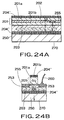
- the waveguide may be made of a material other than semiconductors. This is a structure having, for example, quartz (SiO 2 ) clad and SiN core.
- Figs. 24A and 24B are conceptional diagrams showing cross-sectional configurations of an element employing quartz clad. That is, Fig. 24A is a cross-sectional view taken along the center axis of the waveguide, and Fig. 24B is a cross-sectional view taken along a plane vertical to the waveguide.
- a DBR reflector 204' First grown on a semiconductor substrate 250 are a DBR reflector 204' and an active layer 203 having a gain at the p-n junction. Troublesome crystal growth is required only in this process, and the number of growth steps can be reduced.
- Second-order diffraction gratings 202 are made in the SiN waveguide core 201a.
- a dielectric high-reflectivity multi-layered film 204' made of SiO 2 and Si (silicon).
- an electrode 270 is formed on the bottom surface of the substrate 250.
- a wire 260 is bonded to the transparent electrode 255. Electric current introduced through the transparent electrode 255 is focused into the active layer 203 below the waveguide structure 201 as shown by arrows in Fig. 24B by the current blocking region 253.
- the construction shown in Figs. 24A and 24B can be fabricated easily because the electrically conducting region and the waveguide region can be separated by absolutely different materials.
- the waveguide region may be combination of SiO 2 clad and SiN core explained above, or may be an optical fiber having formed diffraction gratings.
- diffraction gratings may be made in the transparent electrode of ITO, for example, and the clad of SiO 2 or other material may be stacked.
- the step of making the waveguide portion can be executed again without damaging the expensive semiconductor growth wafer even upon a failure in fabrication of the waveguide portion.
- the embodiment has another advantage that, since the waveguide can be made to have a smaller refractive index than semiconductors and may be as large as approximately twice in size, its processing is easy.
- the semiconductor portion can be manufactured much more easily.
- Figs. 25A and 25B are conceptional diagrams showing cross-sectional configurations of an element in which the waveguide is activated by a reverse bias. That is, Fig. 25A is a cross-sectional view taken along the center axis of the waveguide, and Fig. 25B is a cross-sectional view taken along a plane vertical to the waveguide.
- Fig. 25A is a cross-sectional view taken along the center axis of the waveguide
- Fig. 25B is a cross-sectional view taken along a plane vertical to the waveguide.
- component or parts identical or equivalent to those of the specific examples explained with reference to Figs. 15 through 24B are labeled with common reference numerals, and their detailed explanation is omitted.
- the layer between the waveguide structure 201 and the gain region 203 is a ground of n-type InP 280, and its upper and lower layers are p-type layers.
- the waveguide portion 201a (core) is made of a material with a crystalline composition in which the real number portion of the refractive index changes in an electric field, the oscillation wavelength can be adjusted by the electric field. That is, a tunable laser having a wide tunable range can be realized.
- the waveguide portion 201a (core) is made of a material with a crystalline composition in which the imaginary number portion of the refractive index changes in an electric field, the loss changes with electric field.
- This is the same function as that of an electro-absorption modulator.
- Such changes with electric field can be used for modulation of output light.
- it is modulation of the optical loss by an electric field.
- the example shown here can obtain a smooth output waveform less affected by relaxation vibration under a high speed. This corresponds to obtaining a so-called "eye-opened state" when observing the output waveform, and high-speed optical transmission with a very low bit error rate is ensured.
- the laser and the modulator can be integrated.
- Figs. 26A and 26B are conceptional diagrams showing cross-sectional configurations of an optical functional element incorporating a laser (LD) and an optical modulator (EAM). That is, Fig. 26A is a cross-sectional view taken along the longitudinal center axis of its waveguide, and Fig. 26B is a cross-sectional view taken along a transversal plane vertical to the waveguide.
- a so-called direct modulation system in which the current to be introduced into the laser is changed, chirp also occurs due to changes in refractive index.
- EAM which is an electro-absorption modulator
- the core portion 201a of the waveguide 201 has a crystalline composition in which the imaginary number portion of the refractive index changes in an electric field.
- an electric field For example, InGaAsP is used.
- optical loss changed by application of an electric field This is the same function as that of an electro-absorption modulator. Such changes with electric field can be used for optical modulation.
- the extended portion of the waveguide with diffraction gratings (in this portion, diffraction gratings are removed to prevent laser function) is used as an electro-absorption modulator (EAM).
- LD has formed an electrode 292 whereas EAM has formed an electrode 294.
- the structure from the gain region 203 to the waveguide 201a can be made in a single process of crystal growth. Since the waveguide in the present invention is apart from the gain region 203 and DBR 204' and can prevent affection to guided mode propagation, they can be grown in a single step. In the EAM portion, no electric current is injected to the gain region 203 not to excite it. When the gain region 203 is not excited, the absorption ratio increases. However, in the present invention, separately providing the waveguide 201, light can be propagated and modulated through the waveguide 201.
- the waveguide portion of the gain region having diffraction gratings may be a tunable laser within the extent not increasing absorption so much.
- EAM is modulation of optical loss by an electric field.
- the example shown here has the merit that a smooth output waveform less affected by relaxation oscillation can be obtained under a high speed.
- Fig. 27 is a conceptional diagram showing the optical active device according to the embodiment.
- a plurality of radiation mode cavities are provided along the long wavelength 201, and are modulated independently of each other.
- This construction makes it possible to vary pumping of the waveguide 201 in the axial direction of the waveguide when the waveguide 201 is the main oscillator. This also enables tuning of the oscillation wavelength.
- optical intensity along the waveguide axial direction becomes uniform, and oscillation instability by non-uniformity, such as spatial holeburning, can be compensated.
- a plurality of radiation mode cavities are used as major oscillators, they can be modulated independently. Moreover, they may be controlled to be different in oscillation wavelength from each other for application as a light source of wavelength division multiplexing (WDM) to output to the waveguide 201.
- WDM wavelength division multiplexing
- the tuner amplifier shown in Fig. 22 is an optical functional element for dividing and receiving optical signals
- the embodiment shown here can be configured as an optical functional element for multiplexing optical signals and transmitting them to the waveguide, in which the radiation mode cavities are used as wavelength multiplexing laser oscillators. Since the transmitter according to the embodiment is similar in construction to the receiver of Fig. 22, the embodiment is excellent also from the viewpoint of productivity.
- Fig. 28 is a conceptional diagram showing the optical functional element according to the embodiment.
- the embodiment shown here is a modified version of the radiation mode cavity which also has a waveguide function. That is, the optical functional element shown in Fig. 28 is an example in which a cavity for amplifying radiation modes is realized in form of a waveguide gain DBR structure 207.
- the "gain (active) DBR" here means a distributed Bragg reflector having a gain and a wavelength selectivity.
- the amplifier means, reflection means and phase control means are unified into the gain DBR waveguide 207.
- Direction of the DBR waveguide 207 is vertical to the waveguide 201, taking directions of radiation modes into consideration.
- Fig. 29 is a conceptional diagram showing the optical functional element according to the embodiment.
- components or parts identical or equivalent to those of the embodiments explained with reference to Figs. 15 through 28 are labeled with common reference numerals, and their detailed explanation is omitted.
- the embodiment shown here is related to the element shown in Fig. 28. That is, the upper side of the cavity for amplifying radiation modes is formed as a waveguide 201' parallel to the original waveguide 201.
- the waveguide 201' has formed an active region 206' and functions to obtain a gain, that is, has the amplifying function.
- Reflection films 230' are formed on facets.
- Coupling of radiation modes to the waveguide 201' is established by second-order diffraction gratings 202 and similar diffraction gratings 202' formed in the waveguide 201.
- the embodiment shown here is regarded as having a plurality of structures of the waveguide 201 which are coupled to each other by their diffraction gratings.
- a cavity not shown, which extends vertically, may be further provided above the cavity 201'.
- Fig. 30 is a partly cut-out, perspective view of the optical functional element according to the embodiment.
- components or parts identical or equivalent to those of the embodiment explained with reference to Figs. 15 through 29 are labeled with common reference numerals, and their detailed explanation is omitted.
- optical functional element according to the instant embodiment has the construction explained below, following its manufacturing process.
- First stacked on the same n-type InP substrate 501 is an InP buffer layer (not shown) of the same n-type. Thereafter, an waveguide layer with gain (201+206) made of InGaAsP is grown. By patterning it, second-order diffraction gratings 202 are formed on its side surfaces.
- gain regions 203 are also formed as the remainder portions.
- a proton bombarded region 504 for isolation is made.
- the p-side electrode for the waveguide and the p-side electrode 506 for the amplifier is formed on the bottom surface of the substrate.
- the high-reflectivity film 204 is stacked on cleaved facets outside the gain regions 203.
- construction of the present invention can be integrated monolithically on the InP substrate.
- respective functions are integrated in a direction horizontal to the substrate surface.
- the illustrated example is a simple basic element, a plurality of elements can be integrated in arrays.
- Fig. 31 is a perspective view schematically showing the optical functional element according to the embodiment.
- components or parts identical or equivalent to those of the embodiments explained with reference to Figs. 15 through 30 are labeled with common reference numerals, and their detailed explanation is omitted.
- the example shown in fig. 31 is a version using GaAlAs/GaAs materials, and its construction is explained below, following its manufacturing process.
- the multi-layered film 204 may be made by stacking an AlAs layer and a GaAs layer. As to the multi-layered film 204 grown in this manner, reflectance of the AlAs layer can be further increased later by adding an Al oxide by selective oxidation.
- GaAs amplifying layer 203 having a gain, n-type AlAs layer 602, and GaAlAs (mole fraction of Al: 0.3) cladding layer 603.
- active layer 206 is grown subsequently, a GaAlAs (mole fraction of Al: 0.15) waveguide layer 201 is grown.
- second-order diffraction gratings 202 are made. After that, a GaAlAs cladding layer 603 is grown by another crystal growth process.
- GaAs contact layer 604 is grown.
- TJS transverse junction stripe
- an integrated element stacking respective means vertically of the substrate surface is obtained. Additionally, by changing a part of the AlAs layer 602 into an Al oxide film 650 by selective oxidation from a lateral direction by using water vapor, it is possible to configure the active layer 206 and the gain layer 203 to perform insulating function and current blocking function.
- the optical functional element is completed.
- the optical functional element according to the instant embodiment is a surface-type vertical-integrated device. This is applicable also to an array of a plurality of elements, similarly to the optical functional element shown in fig. 30.
- Fig. 32 is a conceptional diagram showing the optical transmission device according to the invention.
- the optical transmission device shown here is an application of any one of DFB lasers shown in Figs. 1 through 5, optical isolators shown in Figs. 7A through 13 or optical functional elements shown in Figs. 15 through 31.
- Connected around an optical transmission/receiving portion 700 is an electronic circuit portion including a drive circuit of LD (laser diode), circuit for measuring optical current from PD (photo diode), APC circuit, and signal generator, for example.
- An optical signal generated in the optical functional element is transferred through an optical fiber 800. It may be transferred by space transmission not using fibers.
- the transmission/receiving device can be small-scaled remarkably. Additionally, since assembly of the transmission/receiving device in its manufacturing process is simplified, the cost is reduced significantly. Furthermore, it is easy to connect to optical fibers. Since the waveguide less variable with temperature can be separated from the gain region with large changes with temperature, the wavelength stability can be maintained.
- III-V compound semiconductors such as InGaAlP and BInGaAlN
- II-IV compound semiconductors such as ZnSe and ZeS
- group IV semiconductors such as SiC
Applications Claiming Priority (6)
| Application Number | Priority Date | Filing Date | Title |
|---|---|---|---|
| JP11052998A JPH11307856A (ja) | 1998-04-21 | 1998-04-21 | 分布帰還型レーザ及びその製造方法 |
| JP11052998 | 1998-04-21 | ||
| JP11488998A JP3595677B2 (ja) | 1998-04-24 | 1998-04-24 | 光アイソレータ、分布帰還型レーザ及び光集積素子 |
| JP11488998 | 1998-04-24 | ||
| JP31484298 | 1998-11-05 | ||
| JP31484298A JP3647656B2 (ja) | 1998-11-05 | 1998-11-05 | 光機能素子及び光通信装置 |
Publications (2)
| Publication Number | Publication Date |
|---|---|
| EP0952472A2 true EP0952472A2 (fr) | 1999-10-27 |
| EP0952472A3 EP0952472A3 (fr) | 2003-07-23 |
Family
ID=27311758
Family Applications (1)
| Application Number | Title | Priority Date | Filing Date |
|---|---|---|---|
| EP99107338A Withdrawn EP0952472A3 (fr) | 1998-04-21 | 1999-04-21 | Elément fonctionnel optique et dispositif transmetteur |
Country Status (2)
| Country | Link |
|---|---|
| US (1) | US6330265B1 (fr) |
| EP (1) | EP0952472A3 (fr) |
Cited By (7)
| Publication number | Priority date | Publication date | Assignee | Title |
|---|---|---|---|---|
| EP0978911A2 (fr) * | 1998-08-04 | 2000-02-09 | Kabushiki Kaisha Toshiba | Dispositif ayant une fonction optique, méthode de fabrication et système de communication optique |
| WO2001099223A2 (fr) * | 2000-06-19 | 2001-12-27 | Clarendon Photonics, Inc. | Resonateur a faibles pertes et procede de fabrication correspondant |
| EP1677131A1 (fr) * | 2004-12-30 | 2006-07-05 | Proximion Fiber Systems AB | Coupleur optique avec réseau de Bragg à fibre optique et cavité de Fabry-Perot |
| WO2010091688A1 (fr) * | 2009-02-11 | 2010-08-19 | Danmarks Tekniske Universitet | Laser à cavité verticale hybride |
| EP3343254A1 (fr) * | 2016-12-30 | 2018-07-04 | Samsung Electronics Co., Ltd. | Dispositif de transmission optique non réciproque et appareil optique comprenant celui-ci |
| WO2021160233A3 (fr) * | 2020-02-14 | 2022-01-13 | SAMIR, Ahmed | Dispositif d'émission de lumière directionnelle ultra-brillante |
| EP3296778B1 (fr) * | 2016-09-20 | 2023-06-21 | Hisense Broadband Multimedia Technologies, Ltd. | Dispositif électroluminescent, module optique et procédé de fabrication associé |
Families Citing this family (38)
| Publication number | Priority date | Publication date | Assignee | Title |
|---|---|---|---|---|
| US6810053B1 (en) * | 1999-08-13 | 2004-10-26 | Wisconsin Alumni Research Foundation | Single mode, single lobe surface emitting distributed feedback semiconductor laser |
| JP3589920B2 (ja) * | 1999-12-10 | 2004-11-17 | Nec化合物デバイス株式会社 | 半導体受光素子 |
| JP3813450B2 (ja) * | 2000-02-29 | 2006-08-23 | 古河電気工業株式会社 | 半導体レーザ素子 |
| JP2002072010A (ja) * | 2000-09-05 | 2002-03-12 | Nippon Sheet Glass Co Ltd | 波長選択性を有する光学素子 |
| JP2002223033A (ja) | 2001-01-26 | 2002-08-09 | Toshiba Corp | 光素子及び光システム |
| JP4101468B2 (ja) * | 2001-04-09 | 2008-06-18 | 豊田合成株式会社 | 発光装置の製造方法 |
| US6643308B2 (en) * | 2001-07-06 | 2003-11-04 | The Furukawa Electric Co., Ltd. | Semiconductor laser device and method for suppressing injection current |
| US6690694B2 (en) * | 2001-11-08 | 2004-02-10 | Intel Corporation | Thermally wavelength tunable lasers |
| ATE295623T1 (de) * | 2001-12-11 | 2005-05-15 | Photonami Corp | Phasenverschobene oberflächenemittierende dfb laserstrukturen mit verstärkenden oder absorbierenden gittern |
| US6885686B2 (en) * | 2002-01-18 | 2005-04-26 | Wisconsin Alumni Research Foundation | High coherent power, two-dimensional surface-emitting semiconductor diode array laser |
| US7457340B2 (en) * | 2002-01-18 | 2008-11-25 | Wisconsin Alumni Research Foundation | High coherent power, two-dimensional surface-emitting semiconductor diode array laser |
| US20030152125A1 (en) * | 2002-02-13 | 2003-08-14 | Junichi Kinoshita | Surface emitting laser and semiconductor light emitting device |
| EP1504632A4 (fr) * | 2002-05-08 | 2008-01-02 | Zeolux Corp | Dispositifs d'affichage faisant intervenir des diodes electroluminescentes a retroaction amelioree |
| US7016569B2 (en) * | 2002-07-31 | 2006-03-21 | Georgia Tech Research Corporation | Back-side-of-die, through-wafer guided-wave optical clock distribution networks, method of fabrication thereof, and uses thereof |
| US20040105476A1 (en) * | 2002-08-19 | 2004-06-03 | Wasserbauer John G. | Planar waveguide surface emitting laser and photonic integrated circuit |
| US6917636B2 (en) * | 2002-08-22 | 2005-07-12 | Xponent Photonics Inc | Grating-stabilized semiconductor laser |
| CN1823456A (zh) * | 2003-06-10 | 2006-08-23 | 福托纳米公司 | 在二阶或高阶分布反馈激光器中抑制空间烧孔的方法和设备 |
| KR100566187B1 (ko) * | 2003-08-20 | 2006-03-29 | 삼성전자주식회사 | 수평방향 레이징 구조를 갖는 이득 고정 반도체 광증폭기및 그제조방법 |
| KR100624415B1 (ko) * | 2003-12-17 | 2006-09-18 | 삼성전자주식회사 | 광디바이스 및 그 제조방법 |
| US7242705B2 (en) * | 2003-12-17 | 2007-07-10 | Palo Alto Research Center, Incorporated | Grating-outcoupled cavity resonator having uni-directional emission |
| US7447246B2 (en) * | 2004-10-27 | 2008-11-04 | Jian-Jun He | Q-modulated semiconductor laser |
| US20060104321A1 (en) * | 2004-11-15 | 2006-05-18 | Lightip Technologies Inc. | Q-modulated semiconductor laser with electro-absorptive grating structures |
| US7983572B2 (en) * | 2005-06-30 | 2011-07-19 | Finisar Corporation | Electro-absorption modulator integrated with a vertical cavity surface emitting laser |
| US7583719B2 (en) * | 2005-08-24 | 2009-09-01 | Applied Optoelectronics, Inc, | Complex-coupled distributed feedback semiconductor laser |
| US8121170B2 (en) * | 2005-08-24 | 2012-02-21 | Applied Optoelectronics, Inc. | Gain-coupled distributed feedback semiconductor laser including first-order and second-order gratings |
| US7453629B2 (en) * | 2005-12-29 | 2008-11-18 | Lucent Technologies Inc. | Semiconductor optical amplifier pulse reshaper |
| US7403552B2 (en) * | 2006-03-10 | 2008-07-22 | Wisconsin Alumni Research Foundation | High efficiency intersubband semiconductor lasers |
| US7457338B2 (en) * | 2006-04-19 | 2008-11-25 | Wisconsin Alumni Research Foundation | Quantum well lasers with strained quantum wells and dilute nitride barriers |
| GB2437784B (en) * | 2006-05-02 | 2011-05-11 | Jian-Jun He | Q-modulated semiconductor laser with electro-absorptive grating structures |
| US7408966B2 (en) * | 2006-08-18 | 2008-08-05 | Wisconsin Alumni Research Foundation | Intersubband quantum box stack lasers |
| JP5074800B2 (ja) * | 2007-03-29 | 2012-11-14 | 古河電気工業株式会社 | 面発光レーザ素子および面発光レーザ素子の製造方法 |
| US7508858B2 (en) * | 2007-04-30 | 2009-03-24 | The Research Foundation Of State University Of New York | Detuned duo-cavity laser-modulator device and method with detuning selected to minimize change in reflectivity |
| DE102007061481A1 (de) * | 2007-09-21 | 2009-04-02 | Osram Opto Semiconductors Gmbh | Strahlungsemittierendes Halbleiterbauelement mit vertikaler Emissionsrichtung und Verfahren zur Herstellung eines strahlungsemittierenden Halbleiterbauelements |
| JP5287460B2 (ja) * | 2009-04-17 | 2013-09-11 | 富士通株式会社 | 半導体レーザ |
| US8391330B2 (en) * | 2009-04-20 | 2013-03-05 | Corning Incorporated | Fracture resistant metallization pattern for semiconductor lasers |
| US20130032825A1 (en) * | 2010-08-31 | 2013-02-07 | John Gilmary Wasserbauer | Resonant Optical Cavity Semiconductor Light Emitting Device |
| JP6998774B2 (ja) * | 2016-01-13 | 2022-02-10 | 古河電気工業株式会社 | 半導体レーザ素子、チップオンサブマウント、および半導体レーザモジュール |
| US11418008B2 (en) * | 2019-03-20 | 2022-08-16 | Electronics And Telecommunications Research Institute | Laser device |
Citations (13)
| Publication number | Priority date | Publication date | Assignee | Title |
|---|---|---|---|---|
| US3898585A (en) * | 1974-01-14 | 1975-08-05 | Ibm | Leaky corrugated optical waveguide device |
| US4006432A (en) * | 1974-10-15 | 1977-02-01 | Xerox Corporation | Integrated grating output coupler in diode lasers |
| US4466694A (en) * | 1978-06-15 | 1984-08-21 | Her Majesty The Queen In Right Of Canada, As Represented By The Minister Of National Defence Of Her Majesty's Canadian Government | Wavelength selective optical coupler |
| JPS63111689A (ja) * | 1986-10-29 | 1988-05-16 | Mitsubishi Electric Corp | 分布帰還型半導体レ−ザ |
| US4754459A (en) * | 1985-09-09 | 1988-06-28 | British Telecommunications Plc | Semiconductor lasers |
| JPH02125670A (ja) * | 1988-11-04 | 1990-05-14 | Nec Corp | 発光素子 |
| US5253262A (en) * | 1990-10-31 | 1993-10-12 | Kabushiki Kaisha Toshiba | Semiconductor laser device with multi-directional reflector arranged therein |
| EP0623980A2 (fr) * | 1993-05-06 | 1994-11-09 | CSELT Centro Studi e Laboratori Telecomunicazioni S.p.A. | Laser à semi-conducteur à émission transversale et couplage à un guide optique |
| US5384797A (en) * | 1992-09-21 | 1995-01-24 | Sdl, Inc. | Monolithic multi-wavelength laser diode array |
| EP0712182A2 (fr) * | 1994-11-14 | 1996-05-15 | Sharp Kabushiki Kaisha | Laser à émission de surface |
| JPH09139540A (ja) * | 1995-11-14 | 1997-05-27 | Nec Corp | 面発光素子およびその製造方法 |
| US5703899A (en) * | 1993-03-01 | 1997-12-30 | Canon Kabushiki Kaisha | Gain-coupling distributed feedback semiconductor and method of producing the same |
| EP0822630A1 (fr) * | 1996-07-30 | 1998-02-04 | Hewlett-Packard Company | Laser à l'émission de surface à cavité verticale à grande longueurs d'ondes infrarouges sur un substrat de GaAs |
Family Cites Families (3)
| Publication number | Priority date | Publication date | Assignee | Title |
|---|---|---|---|---|
| US5111467A (en) * | 1990-09-10 | 1992-05-05 | Tacan Corporation | Hybrid rugate filter assembly for temperature stabilized emission of grating coupled surface emitting lasers |
| FR2741483B1 (fr) * | 1995-11-21 | 1998-01-02 | Thomson Csf | Dispositif optoelectronique a puits quantiques |
| US6031243A (en) * | 1996-10-16 | 2000-02-29 | Geoff W. Taylor | Grating coupled vertical cavity optoelectronic devices |
-
1999
- 1999-04-20 US US09/295,295 patent/US6330265B1/en not_active Expired - Fee Related
- 1999-04-21 EP EP99107338A patent/EP0952472A3/fr not_active Withdrawn
Patent Citations (13)
| Publication number | Priority date | Publication date | Assignee | Title |
|---|---|---|---|---|
| US3898585A (en) * | 1974-01-14 | 1975-08-05 | Ibm | Leaky corrugated optical waveguide device |
| US4006432A (en) * | 1974-10-15 | 1977-02-01 | Xerox Corporation | Integrated grating output coupler in diode lasers |
| US4466694A (en) * | 1978-06-15 | 1984-08-21 | Her Majesty The Queen In Right Of Canada, As Represented By The Minister Of National Defence Of Her Majesty's Canadian Government | Wavelength selective optical coupler |
| US4754459A (en) * | 1985-09-09 | 1988-06-28 | British Telecommunications Plc | Semiconductor lasers |
| JPS63111689A (ja) * | 1986-10-29 | 1988-05-16 | Mitsubishi Electric Corp | 分布帰還型半導体レ−ザ |
| JPH02125670A (ja) * | 1988-11-04 | 1990-05-14 | Nec Corp | 発光素子 |
| US5253262A (en) * | 1990-10-31 | 1993-10-12 | Kabushiki Kaisha Toshiba | Semiconductor laser device with multi-directional reflector arranged therein |
| US5384797A (en) * | 1992-09-21 | 1995-01-24 | Sdl, Inc. | Monolithic multi-wavelength laser diode array |
| US5703899A (en) * | 1993-03-01 | 1997-12-30 | Canon Kabushiki Kaisha | Gain-coupling distributed feedback semiconductor and method of producing the same |
| EP0623980A2 (fr) * | 1993-05-06 | 1994-11-09 | CSELT Centro Studi e Laboratori Telecomunicazioni S.p.A. | Laser à semi-conducteur à émission transversale et couplage à un guide optique |
| EP0712182A2 (fr) * | 1994-11-14 | 1996-05-15 | Sharp Kabushiki Kaisha | Laser à émission de surface |
| JPH09139540A (ja) * | 1995-11-14 | 1997-05-27 | Nec Corp | 面発光素子およびその製造方法 |
| EP0822630A1 (fr) * | 1996-07-30 | 1998-02-04 | Hewlett-Packard Company | Laser à l'émission de surface à cavité verticale à grande longueurs d'ondes infrarouges sur un substrat de GaAs |
Non-Patent Citations (5)
| Title |
|---|
| DZIURA T G ET AL: "Singlemode surface emitting laser using partial mirror disordering" ELECTRONICS LETTERS, vol. 29, no. 14, 8 July 1993 (1993-07-08), pages 1236-1237, XP000392250 UK ISSN: 0013-5194 * |
| MACDOUGAL M H ET AL: "ELECTRICALLY-PUMPED VERTICAL-CAVITY LASERS WITH ALXOY-GAAS REFLECTORS" IEEE PHOTONICS TECHNOLOGY LETTERS, IEEE INC. NEW YORK, US, vol. 8, no. 3, 1 March 1996 (1996-03-01), pages 310-312, XP000582807 ISSN: 1041-1135 * |
| PATENT ABSTRACTS OF JAPAN vol. 014, no. 359 (E-0959), 3 August 1990 (1990-08-03) & JP 02 125670 A (NEC CORP), 14 May 1990 (1990-05-14) * |
| PATENT ABSTRACTS OF JAPAN vol. 1997, no. 09, 30 September 1997 (1997-09-30) -& JP 09 139540 A (NEC CORP), 27 May 1997 (1997-05-27) * |
| WELCH D F ET AL: "HIGH POWER, 16 W, GRATING SURFACE EMITTING LASER WITH A SUPERLATTICE SUBSTRATE REFLECTOR" ELECTRONICS LETTERS, IEE STEVENAGE, GB, vol. 26, no. 11, 24 May 1990 (1990-05-24), pages 757-758, XP000108707 ISSN: 0013-5194 * |
Cited By (16)
| Publication number | Priority date | Publication date | Assignee | Title |
|---|---|---|---|---|
| EP0978911A2 (fr) * | 1998-08-04 | 2000-02-09 | Kabushiki Kaisha Toshiba | Dispositif ayant une fonction optique, méthode de fabrication et système de communication optique |
| EP0978911A3 (fr) * | 1998-08-04 | 2004-02-25 | Kabushiki Kaisha Toshiba | Dispositif ayant une fonction optique, méthode de fabrication et système de communication optique |
| WO2001099223A2 (fr) * | 2000-06-19 | 2001-12-27 | Clarendon Photonics, Inc. | Resonateur a faibles pertes et procede de fabrication correspondant |
| WO2001099223A3 (fr) * | 2000-06-19 | 2003-03-06 | Clarendon Photonics Inc | Resonateur a faibles pertes et procede de fabrication correspondant |
| EP1677131A1 (fr) * | 2004-12-30 | 2006-07-05 | Proximion Fiber Systems AB | Coupleur optique avec réseau de Bragg à fibre optique et cavité de Fabry-Perot |
| WO2006069789A2 (fr) * | 2004-12-30 | 2006-07-06 | Proximion Fiber Systems Ab | Coupleur optique |
| WO2006069789A3 (fr) * | 2004-12-30 | 2006-10-05 | Proximion Fiber Systems Ab | Coupleur optique |
| US9184562B2 (en) | 2009-02-11 | 2015-11-10 | Danmarks Tekniske Universitet | Hybrid vertical-cavity laser |
| WO2010091688A1 (fr) * | 2009-02-11 | 2010-08-19 | Danmarks Tekniske Universitet | Laser à cavité verticale hybride |
| EP3296778B1 (fr) * | 2016-09-20 | 2023-06-21 | Hisense Broadband Multimedia Technologies, Ltd. | Dispositif électroluminescent, module optique et procédé de fabrication associé |
| EP3343254A1 (fr) * | 2016-12-30 | 2018-07-04 | Samsung Electronics Co., Ltd. | Dispositif de transmission optique non réciproque et appareil optique comprenant celui-ci |
| CN108267814A (zh) * | 2016-12-30 | 2018-07-10 | 三星电子株式会社 | 非互易光传输器件及包括其的光学装置 |
| US10670891B2 (en) | 2016-12-30 | 2020-06-02 | Samsung Electronics Co., Ltd. | Nonreciprocal optical transmission device and optical apparatus including the same |
| CN108267814B (zh) * | 2016-12-30 | 2021-03-19 | 三星电子株式会社 | 非互易光传输器件及包括其的光学装置 |
| US11262606B2 (en) | 2016-12-30 | 2022-03-01 | Samsung Electronics Co., Ltd. | Nonreciprocal optical transmission device and optical apparatus including the same |
| WO2021160233A3 (fr) * | 2020-02-14 | 2022-01-13 | SAMIR, Ahmed | Dispositif d'émission de lumière directionnelle ultra-brillante |
Also Published As
| Publication number | Publication date |
|---|---|
| EP0952472A3 (fr) | 2003-07-23 |
| US6330265B1 (en) | 2001-12-11 |
Similar Documents
| Publication | Publication Date | Title |
|---|---|---|
| US6330265B1 (en) | Optical functional element and transmission device | |
| US6088376A (en) | Vertical-cavity-surface-emitting semiconductor devices with fiber-coupled optical cavity | |
| US9312663B2 (en) | Laser device, light modulation device, and optical semiconductor device | |
| EP0735635B1 (fr) | Appareil optique semi-conducteur, sa méthode de commande, appareil source lumineuse et système de communication optique utilisant celui-ci | |
| KR100244821B1 (ko) | 발광소자와 외부변조기의 집적소자 | |
| US6252895B1 (en) | Distributed feedback semiconductor laser in which light intensity distributions differ in different polarization modes, and driving method therefor | |
| US4852108A (en) | Wavelength tunable semiconductor laser with narrow band-pass active filter region | |
| US8787420B2 (en) | Integrated semiconductor laser element | |
| US7190861B2 (en) | Monolithic semiconductor light source with spectral controllability | |
| JP2005538532A (ja) | 傾斜型共振器半導体レーザー(tcsl)及びその製造方法 | |
| US6963597B2 (en) | Grating-outcoupled surface-emitting lasers | |
| WO2013115179A1 (fr) | Élément semi-conducteur optique, élément semi-conducteur optique de type intégré, et module d'éléments semi-conducteurs optiques | |
| JP2003046190A (ja) | 半導体レーザ | |
| JP2019083351A (ja) | 半導体光増幅器、半導体レーザモジュール、および波長可変レーザアセンブリ | |
| US6810067B2 (en) | Single mode grating-outcoupled surface emitting laser with broadband and narrow-band DBR reflectors | |
| JP3647656B2 (ja) | 光機能素子及び光通信装置 | |
| US6888874B2 (en) | Single-wavelength, unequal-length-multi-cavity grating-outcoupled surface emitting laser with staggered tuned distributed Bragg reflectors | |
| US8576472B2 (en) | Optoelectronic device with controlled temperature dependence of the emission wavelength and method of making same | |
| US7092598B2 (en) | Chip-scale WDM system using grating-outcoupled surface-emitting lasers | |
| US6636547B2 (en) | Multiple grating-outcoupled surface-emitting lasers | |
| JP2002270972A (ja) | 半導体光増幅器およびase放射用光源装置および光ゲートアレイおよび波長可変レーザ装置および多波長レーザ装置および光伝送システム | |
| US20020006145A1 (en) | Grating-outcoupled surface-emitting lasers using quantum wells | |
| US11557876B2 (en) | Semiconductor laser | |
| JP2002374037A (ja) | 半導体レーザモジュール、それを用いたファイバ増幅器と光通信システム | |
| US20030103761A1 (en) | Folded light path for planar optical devices |
Legal Events
| Date | Code | Title | Description |
|---|---|---|---|
| PUAI | Public reference made under article 153(3) epc to a published international application that has entered the european phase |
Free format text: ORIGINAL CODE: 0009012 |
|
| 17P | Request for examination filed |
Effective date: 19990421 |
|
| AK | Designated contracting states |
Kind code of ref document: A2 Designated state(s): AT BE CH CY DE DK ES FI FR GB GR IE IT LI LU MC NL PT SE |
|
| AX | Request for extension of the european patent |
Free format text: AL;LT;LV;MK;RO;SI |
|
| PUAL | Search report despatched |
Free format text: ORIGINAL CODE: 0009013 |
|
| AK | Designated contracting states |
Designated state(s): AT BE CH CY DE DK ES FI FR GB GR IE IT LI LU MC NL PT SE |
|
| AX | Request for extension of the european patent |
Extension state: AL LT LV MK RO SI |
|
| STAA | Information on the status of an ep patent application or granted ep patent |
Free format text: STATUS: THE APPLICATION HAS BEEN WITHDRAWN |
|
| 18W | Application withdrawn |
Effective date: 20030822 |