EP0951145A1 - Circuit for the acquisition of analog binary signals - Google Patents
Circuit for the acquisition of analog binary signals Download PDFInfo
- Publication number
- EP0951145A1 EP0951145A1 EP99400879A EP99400879A EP0951145A1 EP 0951145 A1 EP0951145 A1 EP 0951145A1 EP 99400879 A EP99400879 A EP 99400879A EP 99400879 A EP99400879 A EP 99400879A EP 0951145 A1 EP0951145 A1 EP 0951145A1
- Authority
- EP
- European Patent Office
- Prior art keywords
- circuit
- schmitt
- input
- logic
- triggers
- Prior art date
- Legal status (The legal status is an assumption and is not a legal conclusion. Google has not performed a legal analysis and makes no representation as to the accuracy of the status listed.)
- Granted
Links
Images


Classifications
-
- G—PHYSICS
- G11—INFORMATION STORAGE
- G11C—STATIC STORES
- G11C27/00—Electric analogue stores, e.g. for storing instantaneous values
- G11C27/02—Sample-and-hold arrangements
- G11C27/024—Sample-and-hold arrangements using a capacitive memory element
-
- H—ELECTRICITY
- H03—ELECTRONIC CIRCUITRY
- H03K—PULSE TECHNIQUE
- H03K3/00—Circuits for generating electric pulses; Monostable, bistable or multistable circuits
- H03K3/02—Generators characterised by the type of circuit or by the means used for producing pulses
- H03K3/027—Generators characterised by the type of circuit or by the means used for producing pulses by the use of logic circuits, with internal or external positive feedback
- H03K3/037—Bistable circuits
- H03K3/0377—Bistables with hysteresis, e.g. Schmitt trigger
-
- H—ELECTRICITY
- H03—ELECTRONIC CIRCUITRY
- H03K—PULSE TECHNIQUE
- H03K5/00—Manipulating of pulses not covered by one of the other main groups of this subclass
- H03K5/01—Shaping pulses
- H03K5/08—Shaping pulses by limiting; by thresholding; by slicing, i.e. combined limiting and thresholding
-
- H—ELECTRICITY
- H03—ELECTRONIC CIRCUITRY
- H03K—PULSE TECHNIQUE
- H03K5/00—Manipulating of pulses not covered by one of the other main groups of this subclass
- H03K5/125—Discriminating pulses
- H03K5/1252—Suppression or limitation of noise or interference
Definitions
- the present invention relates to signal acquisition binary analog at the input of a digital integrated circuit.
- Schmitt triggers which present a tilt hysteresis with two distinct thresholds: a high threshold at the climb and a low threshold on the descent.
- the Schmitt trigger input digital stage is realized in a cell of the digital integrated circuit.
- it has the disadvantage of having its electrical characteristics, therefore its thresholds of tilting, frozen during the characterization of its integration cell.
- cell characterization is an expensive operation that we try to avoid as much as possible. It is as is usual to define the architecture of an integrated circuit digital ASIC (Application Specific Integrated Circuit in language Anglo-Saxon) prediffused or precharacterized, from a combination of precharacterized cells of various types, established in advance and grouped together in library.
- ASIC Application Specific Integrated Circuit in language Anglo-Saxon
- the designer of an ASIC circuit has therefore, to discretize a binary analog signal, that a choice among a game reduced by several types of digital trigger input stages Schmitt with fixed characteristics, game often limited to two types, one TTL standard, the other CMOS standard. It sometimes happens that from the set of Schmitt trigger input digital stages none are really suitable so unless you do develop a specific cell, which is expensive, the designer of a ASIC circuit must opt for an available type of input stage Schmitt trigger digital with high tilt thresholds and that are not the ones you want but just theirs relatives. The digital integrated circuit obtained then manifests a more high sensitivity to noise or requires a more adaptive stage complex.
- the object of the present invention is to combat this disadvantage by increasing, for an integrated circuit designer digital ASIC, the possibilities of choice of threshold levels of up and down of a digital input stage despite the limitation imposed by a reduced number of digital stage types input to Schmitt trigger precharacterized in library.
- Its object is a circuit for the acquisition of a signal binary analog with multiple Schmitt triggers as input with different tilt thresholds, connected in parallel by their inputs, and followed by at least one logic discretization circuit deducing the state of the binary analog signal from the combination of states output of input Schmitt triggers.
- the discretization logic circuit comprises feedback means allowing a temporary forcing of the level signal input from Schmitt triggers.
- the discretization logic circuit can be used to increase or decrease the apparent hysteresis of two Schmitt triggers having stepped high and low tilt thresholds.
- it When used to increase the apparent hysteresis, it includes a logical rocker changing state on the one hand, during the transition to logical level 1 of the Schmitt trigger having the highest high tilt threshold and on the other hand when switching to logic level 0 of the Schmitt trigger having the lowest tipping threshold.
- Schmitt trigger When used for decrease the apparent hysteresis of two Schmitt triggers having stepped high and low tilting thresholds, it includes a rocker logic changing state on the one hand, when passing to logic level 0 the Schmitt trigger having the highest low tilt threshold and, on the other hand, when switching to logic level 1 of the Schmitt trigger having the lowest high tilt threshold and means for feedback forcing the Schmitt trigger to a high threshold for a short time highest tilting when crossing its high threshold dice crossing up the upper threshold of the other Schmitt trigger by the input signal, and the Schmitt trigger at the low threshold of lowest tipping when crossing its low threshold as soon as crossing down from the low threshold of the other Schmitt trigger by the input signal.
- the discretization logic circuit by allowing select one of the input Schmitt triggers for crossing at the rise of its high threshold and another for crossing at the lowering of its low threshold while ensuring, when it turns out necessary, feedback guaranteeing the sensitivity of these two Schmitt triggers at the crossings of these two thresholds does more than double the freedom of choice of the digital integrated circuit designer ASIC, this freedom of choice being all the greater as the number of types of input Schmitt trigger is high.
- the circuit for the acquisition of a signal binary analog is part of a digital integrated circuit in a case and has its various input Schmitt triggers connected as an input to a same connection pin of the digital integrated circuit box.
- the digital integrated circuit in a housing contains several circuit copies for signal acquisition binary analog each having their different Schmitt triggers input connected to the same pin of the circuit box integrated digital and individual test means of each of the thresholds triggers based on logical door chains of the "no and" type each connected at the outputs of the same type of Schmitt triggers.
- the circuit for the acquisition of a signal binary analog includes, in addition to Schmitt triggers with different switching thresholds, connected in parallel by their inputs, and of the discretization logic circuit which is connected to the outputs of the Schmitt triggers and which deduces the state of the analog signal binary of the combination of the output states of the Schmitt triggers, a digital output filter eliminating transient noise caused by the asynchronous operations of the various Schmitt triggers.
- the circuit for the acquisition of a signal binary analog includes, in addition to Schmitt triggers with different switching thresholds, connected in parallel by their inputs, and of the discretization logic circuit which is connected to the outputs of the Schmitt triggers and which deduces the state of the analog signal binary of the combination of the exit states of the Schmitt triggers, failure detection means detecting prohibited combinations between output states of the various Schmitt triggers.
- the circuit for the acquisition of a signal binary analog includes, in addition to Schmitt triggers with different switching thresholds, connected in parallel by their inputs, and of the discretization logic circuit which is connected to the outputs of the Schmitt triggers and which deduces the state of the analog signal binary of the combination of the exit states of the Schmitt triggers, failure detection means detecting prohibited combinations between output states of the various Schmitt triggers and triggering only when prohibited combinations between states of exit of the various Schmitt triggers beyond a certain duration.
- the circuit for the acquisition of a signal binary analog has several discretization logic circuits different and a circuit for selecting the output of one of your choice discretization logic circuits.
- the circuit for the acquisition of a binary analog signal which will be described, is integrated on the chip of an ASIC digital circuit. It is represented in FIG. 1 behind a purely passive analog stage, outside the ASIC digital integrated circuit chip, bringing the range voltage variation of the binary analog signal across the voltage variation range allowed by the digital integrated circuit ASIC. It essentially comprises, an entrance floor consisting of a bank of Schmitt triggers 1, 2, 3 of different types including inputs are connected in parallel, and an output stage consisting of a circuit discretization logic 4 deducing the state of the binary analog signal the combination of the output states of the Schmitt trigger bank input 1, 2, 3 and possibly acting on the input signal (dotted feedback connection) to raise awareness of triggers Schmitt.
- the passive analog input stage which is outside the circuit integrated digital ASIC, is constituted, in the usual way by a voltage divider bridge with two resistors 5, 6 supplemented by a filtering capacity 7. It serves, as indicated above, to adapt the voltage variation range of the binary analog signal, which is often several tens of volts, at the voltage variation range allowed by the integrated circuit ASIC, which is generally between 0 and 5 volts and sometimes less.
- the Schmitt trigger bank 1, 2, 3 placed at the input of the the actual circuit for acquiring a binary analog signal is made up of at least two different types of Schmitt triggers including the cells in the digital integrated circuit ASIC were precharacterized and are part of a cell library at the layout of the integrated circuit designer. These two types are by example CMOS type with a hysteresis value of around 1.9 volts between the high and low trigger thresholds of a trigger, and the TTL type with a hysteresis value of approximately 0.6 volts between the thresholds of up and down switching of a trigger. Of course, there can be other types of Schmitt trigger with different values hysteresis. It suffices for this that these other types have been precharacterized and appear in the cell library available from the ASIC designer.
- the discretization logic circuit 4 is a logic circuit combinatorial and / or sequential, possibly even of memory type, which deduces the state of the binary analog signal from the combination of states output of the various Schmitt triggers 1, 2, 3. It can be, as shown in Figure 2 followed by a digital noise filter 8 and doubled by a fault detection circuit 9.
- the digital noise filter eliminates transients due to asynchronous operations of the different triggers by Schmitt.
- the filtering capacity 7 of the passive analog stage input then acts as an anti-aliasing filter necessary for good operation of this digital noise filter.
- the fault detection circuit 9 is a logic circuit combinatorial and / or sequential, possibly even of memory type, which locates the prohibited combinations of the output states of the triggers of Schmitt 1, 2, 3 for fault detection purposes. It emits a signal alarm when it finds that a prohibited combination between the output states of the various Schmitt triggers beyond one certain duration.
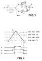
- FIG. 3 illustrates a practical embodiment of a circuit for the acquisition of a binary analog signal in the frequent case, where the cell library available to the circuit designer integrated ASIC contains only two types of Schmitt trigger, one at CMOS standard, the other TTL standard and where you want to increase hysteresis.
- the input Schmitt trigger bank consists of a CMOS 10 Schmitt trigger and a Schmitt trigger to TTL 11 standard and the logic circuit discretization by a storage register 12 active on level.
- the storage register 12 has a given input D carried to the level logic + 1, a registration authorization input e connected to the output of the CMOS standard Schmitt 10 trigger, an additional input priority reset nr connected at the output of the Schmitt trigger 11 to TTL standard and a given Q output.
- the Q output of the storage 12 goes to logic level 1 each time the signal binary analog input crosses the high standard threshold on the rise CMOS and logic level 0 whenever the analog signal entry crosses the lower threshold of the TTL standard when descending.
- the digital circuits of output 27, 28 impose their output level + 1 or 0 on the inputs of the Schmitt triggers 20, 21 due to non-zero output impedance of the analog input stage used for range scaling variation of the binary analog input signal.
- the first storage circuit 22 of the logic circuit of discretization which delivers the output signal on its data output Q, goes to logic level 1 each time the Schmitt trigger 21 at standard TTL switches to high state and logic level 0 each time that the CMOS standard Schmitt 20 trigger switches to the low state.
- the two Schmitt triggers 20, 21 must be CMOS and TTL standards are sensitive to passing one of its threshold low when the high threshold of the other has been crossed, the other of its high threshold when the other's low threshold has been crossed, which implies that they have previously seen the binary analog input signal crossing their other threshold in the opposite direction.
- the first logic gate 24 detects the instants during which the binary analog input signal has crossed by increasing the TTL high threshold but has not yet crossed the CMOS high threshold, or crossed below the low CMOS threshold but did not cross the threshold low TTL. Its output signal "sa1" thus identifies the instants or a forcing may be necessary so as to make it later one of the triggers sensitive to the crossing of its antagonistic threshold.
- the second storage register 23 identifies that of the Schmitt triggers 20, 21 which is likely to be forced. If its release of data Q is at logic level 0, is that the amplitude of the signal binary analog input went below the TTL low threshold without be passed again above the high CMOS threshold and the threshold at force is possibly the high CMOS threshold. If its data output Q is at logic level 1, is that the amplitude of the analog signal input binary passed above the high CMOS threshold without being again passed below the low TTL threshold and the threshold to be forced is possibly the low TTL threshold.
- the second logic gate 25 combines a logic level 0 in output of the second storage register 23 and a logic level 1 at the output of the first logic gate 24 to cause a forcing temporary amplitude of the binary analog input signal beyond from the high trigger threshold of the CMOS standard trigger.
- the third logic gate 26 combines a logic level 1 in output of the second storage register 23 and a logic level 1 at the output of the first logic gate 24 to cause a forcing temporary amplitude of the binary analog input signal in below the low threshold for triggering the TTL standard trigger.
- the diagrams in Figure 6 illustrate the shape of the different signals found at different points in the diagram in Figure 5 for a binary analog input signal S 'evolving between the high threshold CMOS switching threshold and TTL low switching threshold, without achieve so far.
- the CMOS_out curve illustrates the shape of the signal in output of the Schmitt 20 trigger in CMOS standard_accounting for effects of forcing circuits.
- the TTL_out curve illustrates the shape of the signal at the output of the Schmitt 21 trigger in TTL standard taking into account effects of forcing circuits.
- Curve sa 1 illustrates the shape of the output signal of the first logic gate 24. We notice that it goes to logic level 1 each time a forcing in one direction or in the other may be necessary.
- the curve sa2 illustrates the shape of the second logic gate 25 output signal. goes to logic level 1 each time a signal forcing binary analog input above the high CMOS switch threshold may be necessary.
- the curve sa3 illustrates the shape of the signal output of the third logic gate 26. We notice that it goes to the logic level 1 whenever a binary analog signal is forced entry below the low TTL tilt threshold may be necessary.
- the curve sl1 illustrates the shape of the signal on the output of data Q of the second storage register 23 and the OUTPUT curve the form of the signal at the output of the discretization logic circuit.
- first storage register 22 could be replaced by a logic gate of type "or".
- the precise constitution of the circuit discretization logic depends on the result we are looking for, that is to say of the two combinations of Schmitt trigger output states of the input stage which one wishes to associate with the two states of the signal binary analog. It is even possible, when the signal analog binary input can be exchanged, provide a choice between several different selections of high and low thresholds by connecting several different discretization logic circuits in parallel on the outputs of the input trigger bank and having a selector circuit at the outputs of the different discretization logic circuits.
- FIG 7 there is shown very schematically the chip of an integrated circuit 30 on its housing 31 to illustrate the wire connections between the connection pins 32 of the box 31 and the connection pads 33, 34 or "pads" of the chip 30.
- the inputs of Schmitt's triggers are in parallel so it is possible to connect their connection pads 33, 34 to the same pin 32, which limits the number of pins connection of the integrated circuit box.
- the technique of logical door chains of type "no and” called technique of "nand tree” in Anglo-Saxon language.
- FIG. 8 illustrates the implementation of the technique of "nand tree" in the case of a digital integrated circuit ASIC containing three circuits for the acquisition of a binary analog signal 40, respectively 41 and 42 of the same type as that of FIG. 3, having each the inputs of their two Schmitt triggers wired to a same connection terminal 400, respectively 401 and 402 of the housing of the ASIC digital integrated circuit.
- the chain for testing CMOS-type Schmitt triggers presents a first logic gate 50 of type "no and” to two inputs with one input raised to logic level + 1 and the other connected to a specific connection terminal 500 on the circuit box integrated ASIC via a Schmitt trigger.
- first logic gate 50 there comes a second logic gate 51 type "no and” with two inputs, with one input connected to the output of the first logic gate 50 and an input connected to the output of the CMOS-type Schmitt trigger of a first acquisition circuit 40.
- the chain for testing Schmitt triggers of TTL type has a similar structure with different "non” type logic gates and "with two inputs 60, 61, 62, 63, and two connection terminals individual on the case of the integrated circuit ASIC, one 600 for its entry and the other 601 for its exit.
Landscapes
- Physics & Mathematics (AREA)
- Nonlinear Science (AREA)
- Manipulation Of Pulses (AREA)
Abstract
Description
La présente invention concerne l'acquisition de signaux analogiques binaires en entrée d'un circuit intégré numérique.The present invention relates to signal acquisition binary analog at the input of a digital integrated circuit.
Le dialogue entre un calculateur et ses périphériques, ou entre plusieurs calculateurs, ou encore entre un opérateur humain et un calculateur, se fait fréquemment au moyen de signaux électriques analogiques discrets ou booléens évoluant autour de deux seuils de tension qui sont plus ou moins écartés en fonction des marges de bruit tolérées. On se retrouve alors avec des tensions mises en jeu qui peuvent être importantes vis à vis des tensions habituellement admises dans les technologies d'intégration numériques les plus courantes aujourd'hui (tension de 5V) de sorte qu'il faut réaliser une adaptation de tension. Celle-ci fait traditionnellement appel à un étage d'interface analogique à pont diviseur résistif incorporant éventuellement une capacité de filtrage. L'adaptation de tension réalisée, il faut déterminer l'état binaire du signal en comparant sa tension instantanée à un niveau de référence. Cela s'obtient en soumettant le signal issu de l'étage d'interface analogique à un comparateur de niveau réalisé en technologie numérique. Comme les pentes d'évolution des signaux acquis par l'intermédiaire d'un étage d'interface analogique sont souvent très lentes devant les vitesses de commutation des technologies numériques actuelles, il y a un grand risque de mettre en oscillation l'étage d'entrée numérique avec pour conséquence une consommation accrue, un fonctionnement hasardeux et enfin une fiabilité pouvant s'en trouver diminuée. Pour pallier à cela, il est connu d'utiliser, à la place de simples comparateurs de niveau, des triggers de Schmitt qui présentent une hystérésis de basculement avec deux seuils distincts : un seuil haut à la montée et un seuil bas à la descente.The dialogue between a computer and its peripherals, or between several computers, or between a human operator and a computer, is done frequently by means of electrical signals discrete or Boolean analogs evolving around two thresholds of voltage which are more or less spread depending on the noise margins tolerated. We then end up with tensions involved which can be significant with regard to the tensions usually accepted in the most common digital integration technologies today (voltage of 5V) so that an adaptation of voltage. This traditionally uses an interface stage analog with resistive divider bridge possibly incorporating a filtering capacity. The voltage adaptation performed, it is necessary to determine the binary state of the signal by comparing its instantaneous voltage to a level reference. This is achieved by submitting the signal from the floor analog interface to a level comparator made in technology digital. As the slopes of evolution of the signals acquired by through an analog interface stage are often very slow in front of the switching speeds of digital technologies current, there is a great risk of oscillating the input stage digital with consequent increased consumption, a hazardous operation and finally a reliability that can be found diminished. To overcome this, it is known to use, instead of simple level comparators, Schmitt triggers which present a tilt hysteresis with two distinct thresholds: a high threshold at the climb and a low threshold on the descent.
L'étage numérique d'entrée à trigger de Schmitt est réalisé dans une cellule du circuit intégré numérique. De ce fait, il a l'inconvénient d'avoir ses caractéristiques électriques, donc ses seuils de basculement, figées lors de la caractérisation de sa cellule d'intégration. Or, dans les technologies d'intégration, la caractérisation des cellules est une opération coûteuse que l'on cherche à éviter le plus possible. C'est ainsi qu'il est habituel de définir l'architecture d'un circuit intégré numérique ASIC (Application Specific Integrated Circuit en langage anglo-saxon) prédiffusé ou précaractérisé, à partir d'une combinaison de cellules précaractérisées de divers types, établies à l'avance et regroupées en bibliothèque. Le concepteur d'un circuit ASIC n'a donc, pour discrétiser un signal analogique binaire, qu'un choix parmi un jeu réduit de plusieurs types d'étages numériques d'entrée à trigger de Schmitt aux caractéristiques figées, jeu souvent limité à deux types, l'un au standard TTL, l'autre au standard CMOS. Il arrive quelquefois, que parmi le jeu d'étages numériques d'entrée à trigger de Schmitt disponibles, aucun ne convienne réellement de sorte que, sauf à faire développer une cellule spécifique, ce qui est coûteux, le concepteur d'un circuit ASIC doit opter pour un type disponible d'étage d'entrée numérique à trigger de Schmitt ayant des seuils de basculement haut et bas qui ne sont pas ceux souhaités mais qui leur sont simplement proches. Le circuit intégré numérique obtenu manifeste alors une plus grande sensibilité au bruit ou nécessite un étage d'adaptation plus complexe.The Schmitt trigger input digital stage is realized in a cell of the digital integrated circuit. As a result, it has the disadvantage of having its electrical characteristics, therefore its thresholds of tilting, frozen during the characterization of its integration cell. However, in integration technologies, cell characterization is an expensive operation that we try to avoid as much as possible. It is as is usual to define the architecture of an integrated circuit digital ASIC (Application Specific Integrated Circuit in language Anglo-Saxon) prediffused or precharacterized, from a combination of precharacterized cells of various types, established in advance and grouped together in library. The designer of an ASIC circuit has therefore, to discretize a binary analog signal, that a choice among a game reduced by several types of digital trigger input stages Schmitt with fixed characteristics, game often limited to two types, one TTL standard, the other CMOS standard. It sometimes happens that from the set of Schmitt trigger input digital stages none are really suitable so unless you do develop a specific cell, which is expensive, the designer of a ASIC circuit must opt for an available type of input stage Schmitt trigger digital with high tilt thresholds and that are not the ones you want but just theirs relatives. The digital integrated circuit obtained then manifests a more high sensitivity to noise or requires a more adaptive stage complex.
La présente invention a pour but de lutter contre cet inconvénient en augmentant, pour un concepteur de circuit intégré numérique ASIC, les possibilités de choix des niveaux de seuils de basculement haut et bas d'un étage numérique d'entrée malgré la limitation imposée par un nombre réduit de types d'étage numérique d'entrée à trigger de Schmitt précaractérisés en bibliothèque.The object of the present invention is to combat this disadvantage by increasing, for an integrated circuit designer digital ASIC, the possibilities of choice of threshold levels of up and down of a digital input stage despite the limitation imposed by a reduced number of digital stage types input to Schmitt trigger precharacterized in library.
Elle a pour objet un circuit pour l'acquisition d'un signal analogique binaire comportant en entrée plusieurs triggers de Schmitt avec des seuils de basculement différents, connectés en parallèle par leurs entrées, et suivis d'au moins un circuit logique de discrétisation déduisant l'état du signal analogique binaire de la combinaison des états de sortie des triggers de Schmitt d'entrée.Its object is a circuit for the acquisition of a signal binary analog with multiple Schmitt triggers as input with different tilt thresholds, connected in parallel by their inputs, and followed by at least one logic discretization circuit deducing the state of the binary analog signal from the combination of states output of input Schmitt triggers.
Avantageusement, le circuit logique de discrétisation comporte des moyens de rétroaction permettant un forçage temporaire du niveau de signal en entrées des triggers de Schmitt.Advantageously, the discretization logic circuit comprises feedback means allowing a temporary forcing of the level signal input from Schmitt triggers.
Le circuit logique de discrétisation peut être utilisé pour
augmenter ou diminuer l'hystérésis apparent de deux triggers de Schmitt
ayant des seuils haut et bas de basculement étagés. Lorsqu'il est utilisé
pour augmenter l'hystérésis apparent, il comporte une bascule logique
changeant d'état d'une part, lors du passage au niveau logique 1 du
trigger de Schmitt ayant le seuil haut de basculement le plus élevé et
d'autre part lors du passage au niveau logique 0 du trigger de Schmitt
ayant le seuil bas de basculement le plus bas. Lorsqu'il est utilisé pour
diminuer l'hystérésis apparent de deux triggers de Schmitt ayant des
seuils haut et bas de basculement étagés, il comporte une bascule
logique changeant d'état d'une part, lors du passage au niveau logique 0
du trigger de Schmitt ayant le seuil bas de basculement le plus élevé et,
d'autre part, lors du passage au niveau logique 1 du trigger de Schmitt
ayant le seuil haut de basculement le plus bas et des moyens de
rétroaction forçant un court instant le trigger de Schmitt à seuil haut de
basculement le plus élevé au franchissement de son seuil haut dés
franchissement en montant du seuil haut de l'autre trigger de Schmitt
par le signal d'entrée, et le trigger de Schmitt au seuil bas de
basculement le plus bas au franchissement de son seuil bas dès
franchissement en descendant du seuil bas de l'autre trigger de Schmitt
par le signal d'entrée.The discretization logic circuit can be used to
increase or decrease the apparent hysteresis of two Schmitt triggers
having stepped high and low tilt thresholds. When used
to increase the apparent hysteresis, it includes a logical rocker
changing state on the one hand, during the transition to
Le circuit logique de discrétisation en permettant de sélectionner un des triggers de Schmitt d'entrée pour le franchissement à la montée de son seuil haut et un autre pour le franchissement à la descente de son seuil bas tout en assurant, lorsque cela se révèle nécessaire, une rétroaction garantissant la sensibilité de ces deux triggers de Schmitt aux passages de ces deux seuils fait plus que doubler la liberté de choix du concepteur de circuit intégré numérique ASIC, cette liberté de choix étant d'autant plus grande que le nombre de types de trigger de Schmitt d'entrée est élevé.The discretization logic circuit by allowing select one of the input Schmitt triggers for crossing at the rise of its high threshold and another for crossing at the lowering of its low threshold while ensuring, when it turns out necessary, feedback guaranteeing the sensitivity of these two Schmitt triggers at the crossings of these two thresholds does more than double the freedom of choice of the digital integrated circuit designer ASIC, this freedom of choice being all the greater as the number of types of input Schmitt trigger is high.
Avantageusement, le circuit pour l'acquisition d'un signal analogique binaire fait partie d'un circuit intégré numérique en boítier et a ses différents triggers de Schmitt d'entrée raccordés en entrée à une même broche de connexion du boítier du circuit intégré numérique.Advantageously, the circuit for the acquisition of a signal binary analog is part of a digital integrated circuit in a case and has its various input Schmitt triggers connected as an input to a same connection pin of the digital integrated circuit box.
Avantageusement, le circuit intégré numérique en boítier comporte plusieurs exemplaires de circuit pour l'acquisition d'un signal analogique binaire ayant chacun leurs différents triggers de Schmitt d'entrée raccordés en entrée à une même broche du boítier du circuit intégré numérique et des moyens de test individuel de chacun des seuils des triggers à base de chaínes de portes logiques de type "non et" connectées chacune en sorties d'un même type de triggers de Schmitt.Advantageously, the digital integrated circuit in a housing contains several circuit copies for signal acquisition binary analog each having their different Schmitt triggers input connected to the same pin of the circuit box integrated digital and individual test means of each of the thresholds triggers based on logical door chains of the "no and" type each connected at the outputs of the same type of Schmitt triggers.
Avantageusement, le circuit pour l'acquisition d'un signal analogique binaire comporte, en plus des triggers de Schmitt avec des seuils de basculement différents, connectés en parallèle par leurs entrées, et du circuit logique de discrétisation qui est connecté aux sorties des triggers de Schmitt et qui déduit l'état du signal analogique binaire de la combinaison des états de sortie des triggers de Schmitt, un filtre numérique de sortie éliminant les bruits transitoires provoqués par les fonctionnements asynchrones des différents triggers de Schmitt.Advantageously, the circuit for the acquisition of a signal binary analog includes, in addition to Schmitt triggers with different switching thresholds, connected in parallel by their inputs, and of the discretization logic circuit which is connected to the outputs of the Schmitt triggers and which deduces the state of the analog signal binary of the combination of the output states of the Schmitt triggers, a digital output filter eliminating transient noise caused by the asynchronous operations of the various Schmitt triggers.
Avantageusement, le circuit pour l'acquisition d'un signal analogique binaire comporte, en plus des triggers de Schmitt avec des seuils de basculement différents, connectés en parallèle par leurs entrées, et du circuit logique de discrétisation qui est connecté aux sorties des triggers de Schmitt et qui déduit l'état du signal analogique binaire de la combinaison des états de sortie des triggers de Schmitt, des moyens de détection de panne détectant les combinaisons interdites entre états de sortie des différents triggers de Schmitt.Advantageously, the circuit for the acquisition of a signal binary analog includes, in addition to Schmitt triggers with different switching thresholds, connected in parallel by their inputs, and of the discretization logic circuit which is connected to the outputs of the Schmitt triggers and which deduces the state of the analog signal binary of the combination of the exit states of the Schmitt triggers, failure detection means detecting prohibited combinations between output states of the various Schmitt triggers.
Avantageusement, le circuit pour l'acquisition d'un signal analogique binaire comporte, en plus des triggers de Schmitt avec des seuils de basculement différents, connectés en parallèle par leurs entrées, et du circuit logique de discrétisation qui est connecté aux sorties des triggers de Schmitt et qui déduit l'état du signal analogique binaire de la combinaison des états de sortie des triggers de Schmitt, des moyens de détection de panne détectant les combinaisons interdites entre états de sortie des différents triggers de Schmitt et se déclenchant uniquement en cas de maintien de combinaisons interdites entre états de sortie des différents triggers de Schmitt au delà d'une certaine durée.Advantageously, the circuit for the acquisition of a signal binary analog includes, in addition to Schmitt triggers with different switching thresholds, connected in parallel by their inputs, and of the discretization logic circuit which is connected to the outputs of the Schmitt triggers and which deduces the state of the analog signal binary of the combination of the exit states of the Schmitt triggers, failure detection means detecting prohibited combinations between output states of the various Schmitt triggers and triggering only when prohibited combinations between states of exit of the various Schmitt triggers beyond a certain duration.
Avantageusement, le circuit pour l'acquisition d'un signal analogique binaire comporte plusieurs circuits logiques de discrétisation différents et un circuit de sélection de la sortie de l'un au choix de ces circuits logiques de discrétisation. Advantageously, the circuit for the acquisition of a signal binary analog has several discretization logic circuits different and a circuit for selecting the output of one of your choice discretization logic circuits.
D'autres avantages et caractéristiques de l'invention ressortiront de la description ci-après de plusieurs modes de réalisation donnés à titre d'exemple. Cette description sera faite en regard du dessin dans lequel :
- une figure 1 est un schéma de principe général d'un circuit pour l'acquisition d'un signal analogique binaire selon l'invention précédé d'un pont diviseur de tension résistif réalisant une adaptation de tension,
- une figure 2 est un schéma d'un circuit conforme à celui de la figure 1, complété par un filtre numérique antibruit et par un circuit de détection de panne,
- une figure 3 est un schéma d'un circuit pour l'acquisition d'un signal analogique binaire selon l'invention comportant deux types de trigger en entrée, l'un répondant au standard CMOS, l'autre répondant au standard TTL et un circuit logique de discrétisation à base d'un registre de mémorisation permettant de sélectionner le seuil haut CMOS et le seuil bas TTL,
- une figure 4 est un diagramme de courbes illustrant le fonctionnement du circuit de la figure 3,
- une figure 5 est un schéma d'un circuit pour l'acquisition d'un signal analogique binaire selon l'invention comportant deux types de trigger en entrée, l'un répondant au standard CMOS, l'autre au standard TTL et un circuit logique de discrétisation à base de registres de mémorisation et de portes logiques permettant de sélectionner le seuil haut TTL et le seuil bas CMOS,
- une figure 6 est un diagramme de courbes illustrant le fonctionnement du circuit de la figure 5,
- une figure 7 est un schéma illustrant le câblage des plages de connexion d'une puce de circuit intégré ASIC aux plots de connexion de son boítier dans le cas des entrées de trigger d'un circuit pour l'acquisition d'un signal analogique binaire selon l'invention, et
- une figure 8 est un schéma illustrant la configuration d'un dispositif logique de test pour le test des triggers d'entrée d'un circuit pour l'acquisition d'un signal analogique binaire selon l'invention.
- FIG. 1 is a general block diagram of a circuit for the acquisition of a binary analog signal according to the invention preceded by a resistive voltage divider bridge carrying out a voltage adaptation,
- FIG. 2 is a diagram of a circuit conforming to that of FIG. 1, supplemented by a digital noise filter and by a fault detection circuit,
- FIG. 3 is a diagram of a circuit for the acquisition of a binary analog signal according to the invention comprising two types of input trigger, one responding to the CMOS standard, the other responding to the TTL standard and a circuit discretization logic based on a storage register making it possible to select the high CMOS threshold and the low TTL threshold,
- FIG. 4 is a diagram of curves illustrating the operation of the circuit of FIG. 3,
- FIG. 5 is a diagram of a circuit for the acquisition of a binary analog signal according to the invention comprising two types of input trigger, one corresponding to the CMOS standard, the other to the TTL standard and a logic circuit discretization based on storage registers and logic gates allowing the selection of the high TTL threshold and the low CMOS threshold,
- FIG. 6 is a diagram of curves illustrating the operation of the circuit of FIG. 5,
- Figure 7 is a diagram illustrating the wiring of the connection pads of an ASIC integrated circuit chip to the connection pads of its housing in the case of trigger inputs of a circuit for the acquisition of a binary analog signal according to the invention, and
- FIG. 8 is a diagram illustrating the configuration of a logic test device for testing the input triggers of a circuit for the acquisition of a binary analog signal according to the invention.
Le circuit pour l'acquisition d'un signal analogique binaire qui
va être décrit, est intégré sur la puce d'un circuit numérique ASIC. Il est
représenté sur la figure 1 derrière un étage analogique purement passif,
extérieur à la puce du circuit intégré numérique ASIC, mettant la gamme
de variation de tension du signal analogique binaire à l'échelle de la
plage de variation de tension admise par le circuit intégré numérique
ASIC. Il comporte essentiellement, un étage d'entrée constitué d'un
banc de triggers de Schmitt 1, 2, 3 de différents types dont les entrées
sont connectées en parallèle, et un étage de sortie constitué d'un circuit
logique de discrétisation 4 déduisant l'état du signal analogique binaire
de la combinaison des états de sortie du banc de triggers de Schmitt
d'entrée 1, 2, 3 et agissant éventuellement sur le signal d'entrée
(connexion de rétroaction en pointillés) pour sensibiliser les triggers de
Schmitt.The circuit for the acquisition of a binary analog signal which
will be described, is integrated on the chip of an ASIC digital circuit. It is
represented in FIG. 1 behind a purely passive analog stage,
outside the ASIC digital integrated circuit chip, bringing the range
voltage variation of the binary analog signal across the
voltage variation range allowed by the digital integrated circuit
ASIC. It essentially comprises, an entrance floor consisting of a
bank of Schmitt
L'étage analogique passif d'entrée, qui est extérieur au circuit
intégré numérique ASIC, est constitué, de la manière habituelle par un
pont diviseur de tension à deux résistances 5, 6 complété par une
capacité de filtrage 7. Il sert, comme indiqué précédemment, à adapter
la plage de variation de tension du signal analogique binaire, qui est
souvent de plusieurs dizaines de volts, à la plage de variation de tension
admise par le circuit intégré ASIC, qui est en général comprise entre 0 et
5 volts et quelquefois moindre.The passive analog input stage, which is outside the circuit
integrated digital ASIC, is constituted, in the usual way by a
voltage divider bridge with two
Le banc de triggers de Schmitt 1, 2, 3 placé en entrée du
circuit proprement dit d'acquisition d'un signal analogique binaire est
constitué d'au moins deux types différents de triggers de Schmitt dont
les cellules dans le circuit intégré numérique ASIC ont été
précaractérisées et font partie d'une bibliothèque de cellules à la
disposition du concepteur de circuit intégré. Ces deux types sont par
exemple le type CMOS avec une valeur d'hystérésis d'environ 1,9 volts
entre les seuils de basculement haut et bas d'un trigger, et le type TTL
avec une valeur d'hystérésis d'environ 0,6 volts entre les seuils de
basculement haut et bas d'un trigger. Bien entendu, il peut y avoir
d'autres types de trigger de Schmitt avec des valeurs différentes
d'hystérésis. Il suffit pour cela, que ces autres types aient été
précaractérisés et figurent dans la bibliothèque de cellule à disposition
du concepteur de circuit intégré ASIC. The Schmitt trigger
Le circuit logique de discrétisation 4 est un circuit logique
combinatoire et/ou séquentiel, éventuellement même de type mémoire,
qui déduit l'état du signal analogique binaire de la combinaison des états
de sortie des différents triggers de Schmitt 1, 2, 3. Il peut être, comme
représenté, à la figure 2 suivi d'un filtre numérique antibruit 8 et doublé
par un circuit de détection de panne 9.The discretization logic circuit 4 is a logic circuit
combinatorial and / or sequential, possibly even of memory type,
which deduces the state of the binary analog signal from the combination of states
output of the various Schmitt
Le filtre numérique antibruit permet de s'affranchir des transitoires dus aux fonctionnements asynchrones des différents triggers de Schmitt. La capacité de filtrage 7 de l'étage analogique passif d'entrée joue alors le rôle de filtre anti-repliement nécessaire au bon fonctionnement de ce filtre numérique antibruit.The digital noise filter eliminates transients due to asynchronous operations of the different triggers by Schmitt. The filtering capacity 7 of the passive analog stage input then acts as an anti-aliasing filter necessary for good operation of this digital noise filter.
Le circuit de détection de panne 9 est un circuit logique combinatoire et/ou séquentiel, éventuellement même de type mémoire, qui repère les combinaisons interdites des états de sortie des triggers de Schmitt 1, 2, 3 à des fins de détection de panne. Il émet un signal d'alarme lorsqu'il constate le maintien d'une combinaison interdite entre les états de sortie des différents triggers de Schmitt au delà d'une certaine durée.The fault detection circuit 9 is a logic circuit combinatorial and / or sequential, possibly even of memory type, which locates the prohibited combinations of the output states of the triggers of Schmitt 1, 2, 3 for fault detection purposes. It emits a signal alarm when it finds that a prohibited combination between the output states of the various Schmitt triggers beyond one certain duration.
La figure 3 illustre un mode de réalisation pratique d'un circuit
pour l'acquisition d'un signal analogique binaire dans le cas fréquent, où
la bibliothèque de cellules à la disposition du concepteur de circuit
intégré ASIC ne renferme que deux types de trigger de Schmitt, l'un au
standard CMOS, l'autre au standard TTL et où l'on désire augmenter
l'hystérésis. On profite alors de l'étagement des seuils de basculement
haut et bas des triggers de Schmitt de type CMOS et TTL résultant du
fait que le seuil haut de basculement CMOS est supérieur au seuil haut
de basculement TTL qui est lui même supérieur au seuil bas de
basculement CMOS lui même supérieur au seuil bas de basculement TTL
et l'on choisit d'avoir pour seuil haut de basculement le seuil haut de
basculement au standard CMOS qui est le plus haut des seuils, et pour
seuil bas de basculement le seuil bas de basculement du standard TTL
qui est le plus bas des seuils. Le banc de triggers de Schmitt d'entrée
est constitué d'un trigger de Schmitt au standard CMOS 10 et d'un
trigger de Schmitt au standard TTL 11 et le circuit logique de
discrétisation par un registre de mémorisation 12 actif sur niveau. Le
registre de mémorisation 12 a une entrée donnée D portée au niveau
logique + 1, une entrée d'autorisation d'inscription e connectée en sortie
du trigger de Schmitt 10 au standard CMOS, une entrée complémentée
de remise à zéro prioritaire nr connectée en sortie du trigger de Schmitt
11 au standard TTL et une sortie donnée Q. La sortie Q du registre de
mémorisation 12 passe au niveau logique 1 chaque fois que le signal
analogique binaire d'entrée franchit à la montée le seuil haut du standard
CMOS et au niveau logique 0 chaque fois que le signal analogique
d'entrée franchit à la descente le seuil bas du standard TTL. On obtient
ainsi, pour le circuit pour l'acquisition d'un signal analogique binaire un
seuil haut équivalent au plus haut des seuils hauts et un seuil bas
équivalent au plus haut des seuils bas de ses triggers de Schmitt.FIG. 3 illustrates a practical embodiment of a circuit
for the acquisition of a binary analog signal in the frequent case, where
the cell library available to the circuit designer
integrated ASIC contains only two types of Schmitt trigger, one at
CMOS standard, the other TTL standard and where you want to increase
hysteresis. We then take advantage of the staggering of the tilting thresholds
top and bottom of CMOS and TTL type Schmitt triggers resulting from
causes the high CMOS failover threshold to be greater than the high threshold
TTL switchover which is itself higher than the low threshold of
CMOS switching itself higher than the low TTL switching threshold
and we choose to have the upper tilting threshold the upper threshold of
switching to the CMOS standard which is the highest of the thresholds, and for
low tipping threshold the low tipping threshold of the TTL standard
which is the lowest of the thresholds. The input Schmitt trigger bank
consists of a
La figure 4 est un diagramme de courbes qui illustre ce fonctionnement. On y distingue :
- un signal d'entrée S de forme triangulaire franchissant au cours du temps l'ensemble des quatre seuils de basculement des triggers de Schmitt au standard CMOS et TTL à la montée puis à la descente,
- le signal e qui résulte, en sortie du trigger au
standard CMOS 10, de l'application du signal d'entrée S et que l'on retrouve sur l'entrée d'autorisation d'inscription e du registre de mémorisation 12, - le signal nr qui résulte, en sortie du trigger
au standard TTL 11, de l'application du signal d'entrée S et que l'on retrouve sur l'entrée complémentée de remise à zéro prioritaire nr du registre de mémorisation 12, et - le signal Q qui résulte en sortie Q du registre de mémorisation 12, de l'application du signal d'entrée S.
- an input signal S of triangular shape crossing over time all of the four thresholds for switching Schmitt triggers to CMOS and TTL standard on ascent then descent,
- the signal e which results, at the output of the CMOS
standard trigger 10, from the application of the input signal S and which is found on the entry for authorization of registration e of thestorage register 12, - the signal nr which results, at the output of the TTL
standard trigger 11, from the application of the input signal S and which is found on the supplemented priority reset input nr of thestorage register 12, and - the signal Q which results at output Q from the
storage register 12, from the application of the input signal S.
On remarque qu'il n'est pas utile de sensibiliser les triggers aux passages des seuils de basculement retenus car ils le sont nécessairement puisque les seuils de basculement retenus encadrent les deux autres seuils de basculement et que leurs franchissements successifs impliquent ceux des deux autres seuils de basculement.We notice that it is not useful to sensitize the triggers when crossing the changeover thresholds chosen because they are necessarily since the changeover thresholds used frame the two other tipping thresholds and that their crossings successive involve those of the other two switching thresholds.
Le même résultat aurait pu être obtenu en remplaçant le
registre de mémorisation 12 du circuit logique de discrétisation par une
porte logique de type "et". The same result could have been obtained by replacing the
Si l'on souhaite au contraire diminuer l'hystérésis, c'est-à-dire sélectionner pour seuil haut de basculement le seuil haut du trigger de Schmitt au standard TTL qui est le plus bas des seuils haut de basculement et pour seuil bas de basculement le seuil bas du trigger de Schmitt au standard CMOS qui est le plus haut des seuils bas de basculement, il ne suffit pas d'échanger les triggers de Schmitt aux standard CMOS et TTL. Il faut aussi compléter le montage conformément à la figure 5 d'une part, pour obliger le trigger au standard CMOS à seuil haut de basculement le plus élevé à basculer à l'état haut au franchissement en montée du seuil haut de basculement du trigger au standard TTL car le signal analogique binaire d'entrée peut franchir à la montée le seuil haut de basculement TTL sans atteindre le seuil haut de basculement CMOS et d'autre part, pour obliger le trigger au standard TTL à seuil bas de basculement le plus bas à basculer à l'état bas au franchissement en descente du seuil bas de basculement du trigger au standard CMOS car le signal analogique binaire d'entrée peut franchir à la descente le seuil bas de basculement du trigger au standard CMOS sans atteindre le seuil bas de basculement TTL.If on the contrary one wishes to decrease the hysteresis, that is to say select the high trigger threshold for the switching threshold Schmitt standard TTL which is the lowest of the high thresholds toggling and for the low switching threshold the low threshold of the trigger Schmitt CMOS standard which is the highest of the low thresholds switching, it's not enough to swap Schmitt triggers to CMOS and TTL standard. It is also necessary to complete the assembly on the one hand, to force the trigger to CMOS standard with the highest tilting threshold the highest to tilt at the high state when crossing the high tilting threshold trigger to TTL standard because the binary analog input signal can crossing the high TTL tilting threshold when climbing without reaching the high CMOS switching threshold and secondly, to force the trigger at the TTL standard with the lowest tilting threshold to be tilted at the low state when going downhill from the low tilting threshold of the CMOS standard trigger because the binary analog input signal can when going downhill, crossing the low threshold for switching the trigger to standard CMOS without reaching the TTL low threshold.
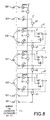
On distingue sur cette figure 5, l'étage analogique passif d'entrée, extérieur au circuit intégré numérique ASIC, constitué du pont diviseur de tension à deux résistances 5, 6 complété par la capacité de filtrage 7. La sortie de cet étage analogique passif mène à un banc de deux triggers de Schmitt d'entrée, l'un 20 au standard CMOS et l'autre 21 au standard TTL, intercalés devant un circuit logique de discrétisation qui comporte :
- un premier registre de mémorisation 22 actif sur niveau, avec
une entrée donnée D portée au niveau logique + 1, une entrée
d'autorisation d'inscription e connectée en sortie du
trigger de Schmitt 21 au standard TTL, une entrée complémentée de remise à zéro prioritaire nr connectée en sortie dutrigger de Schmitt 20 au standard CMOS et une sortie de donnée Q délivrant le signal de sortie général du montage, - un deuxième registre de mémorisation 23 actif sur niveau,
avec une entrée donnée D portée au niveau logique + 1, une entrée
d'autorisation d'inscription e connectée en sortie du
trigger de Schmitt 20 au standard CMOS, une entrée complémentée de remise à zéro prioritaire nr connectée en sortie dutrigger de Schmitt 21 au standard TTL et une sortie de donnée Q, - une première porte logique 24 de type "et" à deux entrées
dont une est complémentée, connectée par son entrée complémentée à
la sortie du
trigger de Schmitt 20 au standard CMOS et par son entrée non complémentée à la sortie dutrigger de Schmitt 21 au standard TTL, - une deuxième porte logique 25 de type "et" à deux entrées dont une est complémentée, connectée par son entrée complémentée à la sortie de donnée Q du deuxième registre de mémorisation 23 et par son entrée non complémentée à la sortie de la première porte logique 24,
- une troisième porte logique 26 de type "et" à deux entrées non complémentées connectées l'une à la sortie de donnée Q du deuxième registre de mémorisation 23 et l'autre à la sortie de la première porte logique 24,
- un premier circuit numérique de sortie 27 à trois états avec
une entrée de donnée portée au niveau logique + 1, une entrée
d'inhibition connectée à la sortie de la deuxième porte logique 25 et une
sortie de donnée connectée en réaction sur l'entrée du
trigger de Schmitt 20 au standard CMOS, et - un deuxième circuit numérique de sortie 28 à trois états avec
une entrée de donnée portée au niveau logique 0, une entrée d'inhibition
connectée à la sortie de la troisième porte logique 26 et une sortie de
donnée connectée en réaction sur l'entrée du
trigger de Schmitt 21 au standard TTL.
- a
first storage register 22 active on level, with a given input D raised tologic level + 1, a registration authorization input e connected at the output of theSchmitt trigger 21 to TTL standard, an input complemented by resetting to zero priority nr connected at the output of theSchmitt trigger 20 to CMOS standard and a data output Q delivering the general output signal of the assembly, - a
second storage register 23 active on level, with a given input D brought tologic level + 1, a registration authorization input e connected at the output of theSchmitt trigger 20 to CMOS standard, an input complemented by resetting to zero priority nr connected at the output of theSchmitt trigger 21 to TTL standard and a data output Q, - a
first logic gate 24 of type "and" with two inputs, one of which is complemented, connected by its input complemented at the output of theSchmitt trigger 20 with CMOS standard and by its input not complemented with the output of theSchmitt trigger 21 with standard TTL, - a
second logic gate 25 of type "and" with two inputs, one of which is complemented, connected by its input complemented to the data output Q of thesecond storage register 23 and by its input not complemented at the output of thefirst logic gate 24 , - a
third logic gate 26 of type "and" with two non-complemented inputs connected one to the data output Q of thesecond storage register 23 and the other to the output of thefirst logic gate 24, - a first three-state
digital output circuit 27 with a data input brought tologic level + 1, a muting input connected to the output of thesecond logic gate 25 and a data output connected in reaction to the input of theCMOS standard Schmitt 20 trigger, and - a second three-state
digital output circuit 28 with a data input brought to logic level 0, a muting input connected to the output of thethird logic gate 26 and a data output connected in reaction to the input of the trigger fromSchmitt 21 to TTL standard.
Lorsqu'ils ne sont pas inhibés, les circuits numériques de
sortie 27, 28 imposent leur niveau de sortie + 1 ou 0 aux entrées des
triggers de Schmitt 20, 21 en raison de l'impédance de sortie non nulle
de l'étage analogique d'entrée utilisé pour la mise à l'échelle de la plage
de variation du signal analogique binaire d'entrée.When not inhibited, the digital circuits of
Le premier circuit de mémorisation 22 du circuit logique de
discrétisation, qui délivre le signal de sortie sur sa sortie de donnée Q,
passe au niveau logique 1 chaque fois que le trigger de Schmitt 21 au
standard TTL bascule à l'état haut et au niveau logique 0 chaque fois
que le trigger de Schmitt 20 au standard CMOS bascule à l'état bas. On
remarque que pour obtenir un fonctionnement en trigger de Schmitt avec
comme seuil haut celui du standard TTL et comme seuil bas celui du
standard CMOS, il faut que les deux triggers de Schmitt 20, 21 aux
standards CMOS et TTL soient sensibles au passage l'un de son seuil
bas lorsque le seuil haut de l'autre a été franchi, l'autre de son seuil haut
lorsque le seuil bas de l'autre a été franchi, ce qui implique qu'ils aient
vu auparavant le signal analogique binaire d'entrée franchir leur autre
seuil dans le sens opposé. Cette condition n'est pas nécessairement
réalisée pour toutes les formes d'ondes du signal analogique binaire
d'entrée en particulier si l'excursion du signal ne traverse pas l'ensemble
des seuils. Pour pallier cet inconvénient, on complète le premier registre
de mémorisation 22 par des circuits de forçage qui modifient un cours
instant l'amplitude du signal analogique binaire d'entrée pour garantir la
sensibilité des triggers de Schmitt 20, 21 aux franchissements des seuils
haut TTL et bas CMOS.The
La première porte logique 24 détecte les instants durant
lesquels le signal analogique binaire d'entrée a franchi en montant le
seuil haut TTL mais n'a pas encore franchi le seuil haut CMOS, ou bien a
franchi en descendant le seuil bas CMOS mais n'a pas franchi le seuil
bas TTL. Son signal de sortie "sa1" repère ainsi les instants ou un
forçage peut se révéler nécessaire de manière à rendre ultérieurement
l'un des triggers sensible au franchissement de son seuil antagoniste.The
Le deuxième registre de mémorisation 23 identifie celui des
triggers de Schmitt 20, 21 qui est susceptible d'être forcé. Si sa sortie
de donnée Q est au niveau logique 0, c'est que l'amplitude du signal
analogique binaire d'entrée est passée en dessous du seuil bas TTL sans
être encore repassée au dessus du seuil haut CMOS et que le seuil à
forcer est éventuellement le seuil haut CMOS. Si sa sortie de donnée Q
est au niveau logique 1, c'est que l'amplitude du signal analogique
binaire d'entrée est passée au dessus du seuil haut CMOS sans être
encore repassée en dessous du seuil bas TTL et que le seuil à forcer est
éventuellement le seuil bas TTL.The
La deuxième porte logique 25 combine un niveau logique 0 en
sortie du deuxième registre de mémorisation 23 et un niveau logique 1
en sortie de la première porte logique 24 pour provoquer un forçage
temporaire de l'amplitude du signal analogique binaire d'entrée au-delà
du seuil haut de basculement du trigger au standard CMOS.The
La troisième porte logique 26 combine un niveau logique 1 en
sortie du deuxième registre de mémorisation 23 et un niveau logique 1
en sortie de la première porte logique 24 pour provoquer un forçage
temporaire de l'amplitude du signal analogique binaire d'entrée en
dessous du seuil bas de basculement du trigger au standard TTL.The
Les diagrammes de la figure 6 illustrent la forme des différents
signaux que l'on retrouve en différents points du schéma de la figure 5
pour un signal analogique binaire d'entrée S' évoluant entre le seuil haut
de basculement CMOS et le seuil bas de basculement TTL, sans les
atteindre pour autant. La courbe CMOS_out illustre la forme du signal en
sortie du trigger de Schmitt 20 au standard CMOS_compte tenu des
effets des circuits de forçage. La courbe TTL_out illustre la forme du
signal en sortie du trigger de Schmitt 21 au standard TTL compte tenu
des effets des circuits de forçage. La courbe sa 1 illustre la forme du
signal de sortie de la première porte logique 24. On remarque qu'elle
passe au niveau logique 1 à chaque fois qu'un forçage dans un sens ou
dans l'autre peut s'avérer nécessaire. La courbe sa2 illustre la forme du
signal de sortie de la deuxième porte logique 25. On remarque qu'elle
passe au niveau logique 1 chaque fois qu'un forçage du signal
analogique binaire d'entrée au-delà du seuil haut de basculement CMOS
peut s'avérer nécessaire. La courbe sa3 illustre la forme du signal de
sortie de la troisième porte logique 26. On remarque qu'elle passe au
niveau logique 1 chaque fois qu'un forçage du signal analogique binaire
d'entrée en deçà du seuil bas de basculement TTL peut s'avérer
nécessaire. La courbe sl1 illustre la forme du signal sur la sortie de
donnée Q du deuxième registre de mémorisation 23 et la courbe SORTIE
la forme du signal en sortie du circuit logique de discrétisation.The diagrams in Figure 6 illustrate the shape of the different
signals found at different points in the diagram in Figure 5
for a binary analog input signal S 'evolving between the high threshold
CMOS switching threshold and TTL low switching threshold, without
achieve so far. The CMOS_out curve illustrates the shape of the signal in
output of the
On remarque que le premier registre de mémorisation 22
pourrait être remplacé par une porte logique de type "ou".Note that the
D'une façon plus générale, la constitution précise du circuit logique de discrétisation dépend du résultat que l'on recherche, c'est-à-dire des deux combinaisons des états de sortie des triggers de Schmitt de l'étage d'entrée que l'on désire associer aux deux états du signal analogique binaire. Il est même envisageable, lorsque le signal analogique binaire d'entrée peut être échangé, de prévoir un choix entre plusieurs sélections différentes de seuils haut et bas en connectant plusieurs circuits logiques de discrétisation différents en parallèle sur les sorties du banc de triggers d'entrée et en disposant un circuit sélecteur en sorties des différents circuits logiques de discrétisation.More generally, the precise constitution of the circuit discretization logic depends on the result we are looking for, that is to say of the two combinations of Schmitt trigger output states of the input stage which one wishes to associate with the two states of the signal binary analog. It is even possible, when the signal analog binary input can be exchanged, provide a choice between several different selections of high and low thresholds by connecting several different discretization logic circuits in parallel on the outputs of the input trigger bank and having a selector circuit at the outputs of the different discretization logic circuits.
Sur la figure 7, on a représenté de manière très schématique
la puce d'un circuit intégré 30 sur son boítier 31 pour illustrer les
connexions par fils conducteur entre les broches de connexion 32 du
boítier 31 et les plages de connexion 33, 34 ou "pads" de la puce 30.
Dans le cas du circuit pour l'acquisition d'un signal analogique binaire,
les entrées des triggers de Schmitt sont en parallèle si bien qu'il est
possible de relier leurs plages de connexion 33, 34 à une même broche
de connexion 32, ce qui permet de limiter le nombre de broches de
connexion du boítier du circuit intégré. Dans ce cas, pour conserver la
capacité de tester en production les seuils de chacun des triggers, on
utilise la technique des chaínes de portes logique de type "non et" dite
technique du "nand tree" en langage anglo-saxon. Dans cette
technique, on utilise autant de chaínes de portes logiques de type "non
et" qu'il y a de triggers de Schmitt connectés en parallèle à l'entrée des
circuits d'acquisition de signal analogique binaire.In Figure 7, there is shown very schematically
the chip of an
La figure 8 illustre la mise en oeuvre de la technique du
"nand tree" dans le cas d'un circuit intégré numérique ASIC renfermant
trois circuits pour l'acquisition d'un signal analogique binaire 40,
respectivement 41 et 42 du même type que celui de la figure 3, ayant
chacun les entrées de leurs deux triggers de Schmitt câblées à une
même borne de connexion 400, respectivement 401 et 402 du boítier
du circuit intégré numérique ASIC. Il y a deux chaínes de portes logiques
de type "non et" : une première 50, 51, 52, 53 pour tester les triggers
de Schmitt de type CMOS et une deuxième 60, 61, 62, 63 pour tester
les triggers de Schmitt de type TTL.FIG. 8 illustrates the implementation of the technique of
"nand tree" in the case of a digital integrated circuit ASIC containing
three circuits for the acquisition of a
La chaíne pour tester les triggers de Schmitt de type CMOS
présente une première porte logique 50 de type "non et" à deux
entrées avec une entrée portée au niveau logique + 1 et l'autre
raccordée à une borne de connexion spécifique 500 du boítier du circuit
intégré ASIC par l'intermédiaire d'un trigger de Schmitt. A la suite de
cette première porte logique 50, il vient une deuxième porte logique 51
de type "non et " à deux entrées, avec une entrée raccordée à la sortie
de la première porte logique 50 et une entrée connectée à la sortie du
trigger de Schmitt de type CMOS d'un premier circuit d'acquisition 40.
A la suite de cette deuxième porte logique 51, il vient une troisième
porte logique 52 de type "non et" à deux entrées, avec une entrée
raccordée à la sortie de la deuxième porte logique 51 et une entrée
connectée à la sortie du trigger de Schmitt de type CMOS d'un
deuxième circuit d'acquisition 41. A la suite de cette troisième porte
logique 52, il vient d'autres portes logiques 53 de type "non et" à
deux entrées raccordées de la même manière jusqu'à avoir fait le tour
des triggers de Schmitt de type CMOS de tous les circuits d'acquisition
40, 41, 42, la dernière 53 ayant sa sortie raccordée à une borne de
connexion individuelle 501 du boítier du circuit intégré ASIC.The chain for testing CMOS-type Schmitt triggers
presents a
La chaíne pour tester les triggers de Schmitt de type TTL a
une structure analogue avec différentes portes logiques de type "non
et" à deux entrées 60, 61, 62, 63, et deux bornes de connexion
individuelle sur le boítier du circuit intégré ASIC, l'une 600 pour son
entrée et l'autre 601 pour sa sortie.The chain for testing Schmitt triggers of TTL type has
a similar structure with different "non" type logic gates
and "with two
Au cours d'un test au moyen de l'une des chaínes, toutes les
entrées de la chaíne sont portées initialement au niveau logique + 1.
Dans un premier temps, un niveau logique 0 est progressivement
appliqué sur toutes les entrées de la chaíne en allant du début vers la fin
de la chaíne. Puis, dans un deuxième temps un niveau logique + 1 est
appliqué progressivement sur toutes les entrées de la chaíne en allant de
la fin vers le début de la chaíne. Au cours de ces modifications
progressives des niveaux logiques appliqués aux entrées de la chaíne on
doit constater des commutations de niveau logique en sortie de chaíne
qui sont dues chacune à la commutation isolée à la montée ou à la
descente de l'un des triggers de Schmitt sous test et qui permettent en
conséquence d'apprécier individuellement les seuils haut et bas de ces
triggers.During a test using one of the chains, all
inputs of the chain are initially brought to the
Claims (12)
Applications Claiming Priority (2)
| Application Number | Priority Date | Filing Date | Title |
|---|---|---|---|
| FR9804859A FR2777717B1 (en) | 1998-04-17 | 1998-04-17 | CIRCUIT FOR THE ACQUISITION OF BINARY ANALOG SIGNALS |
| FR9804859 | 1998-04-17 |
Publications (2)
| Publication Number | Publication Date |
|---|---|
| EP0951145A1 true EP0951145A1 (en) | 1999-10-20 |
| EP0951145B1 EP0951145B1 (en) | 2004-03-03 |
Family
ID=9525386
Family Applications (1)
| Application Number | Title | Priority Date | Filing Date |
|---|---|---|---|
| EP99400879A Expired - Lifetime EP0951145B1 (en) | 1998-04-17 | 1999-04-09 | Circuit for the acquisition of analog binary signals |
Country Status (5)
| Country | Link |
|---|---|
| US (1) | US6204786B1 (en) |
| EP (1) | EP0951145B1 (en) |
| CA (1) | CA2267535A1 (en) |
| DE (1) | DE69915155D1 (en) |
| FR (1) | FR2777717B1 (en) |
Cited By (3)
| Publication number | Priority date | Publication date | Assignee | Title |
|---|---|---|---|---|
| FR2827676A1 (en) * | 2001-07-23 | 2003-01-24 | Bosch Gmbh Robert | Power stage diagnostic system uses supply divider and two processor inputs |
| EP2538414A1 (en) * | 2011-06-23 | 2012-12-26 | Thales | Memory device correcting the effect of high-energy particle collisions |
| WO2014070550A1 (en) * | 2012-11-05 | 2014-05-08 | Sandisk Technologies Inc. | High speed buffer with high noise immunity |
Families Citing this family (19)
| Publication number | Priority date | Publication date | Assignee | Title |
|---|---|---|---|---|
| FR2822319B1 (en) * | 2001-03-16 | 2003-05-30 | Thomson Csf | VARIABLE SIZE INFORMATION FRAME SWITCH FOR ON-BOARD SECURITY NETWORKS |
| FR2828046B1 (en) * | 2001-07-27 | 2003-10-10 | Thales Sa | TASK MANAGEMENT METHOD FOR A PACKET SWITCHING ROUTER AUTOMATION PART OF A SECURE PACKET SWITCHED TRANSMISSION NETWORK |
| US6805225B2 (en) * | 2002-04-08 | 2004-10-19 | Roberta Freedman | Combination travel and laundry bag |
| FR2840482B1 (en) * | 2002-05-28 | 2004-10-15 | Thales Sa | METHOD FOR RECONSTITUTING MESSAGES ROUTED BY ONE OR MORE PACKET TRANSMISSION NETWORKS |
| JP3809585B2 (en) * | 2004-02-10 | 2006-08-16 | 日本テキサス・インスツルメンツ株式会社 | Hysteresis type input circuit |
| FR2900749B1 (en) * | 2006-05-05 | 2008-07-25 | Thales Sa | METHOD AND DEVICE FOR SECURING THE MEMORY OF A COMPUTER AGAINST ERRORS DUE TO RADIATION |
| FR2933829B1 (en) * | 2008-07-08 | 2015-08-07 | Thales Sa | DEVICE AND METHOD FOR DETECTING THE DIGITAL ORIGIN OF AN ANALOG SIGNAL |
| ITTO20130307A1 (en) | 2013-04-17 | 2014-10-18 | Itt Italia Srl | METHOD TO REALIZE A BRAKE ELEMENT, IN PARTICULAR A BRAKE PAD, SENSORIZED, SENSORED BRAKE PAD, VEHICLE BRAKE SYSTEM AND ASSOCIATED METHOD |
| TWI498572B (en) * | 2013-05-07 | 2015-09-01 | Wistron Corp | Method of automatically detecting the output voltage of the tuner of the dvb-s reception device, adapter and dvb-s reception device |
| WO2016189150A1 (en) * | 2015-05-28 | 2016-12-01 | Itt Italia S.R.L. | Braking device for vehicles comprising a conditioner for conditioning the electrical signal coming from at least one piezoceramic sensor of the braking device |
| ITUB20151184A1 (en) * | 2015-05-28 | 2016-11-28 | Itt Italia Srl | CONDITIONER OF THE ELECTRIC SIGNAL COMING FROM AT LEAST ONE PIEZOCERAMIC SENSOR OF A BRAKING DEVICE FOR VEHICLES |
| US9939035B2 (en) | 2015-05-28 | 2018-04-10 | Itt Italia S.R.L. | Smart braking devices, systems, and methods |
| ITUB20153709A1 (en) | 2015-09-17 | 2017-03-17 | Itt Italia Srl | DATA ANALYSIS AND MANAGEMENT DEVICE GENERATED BY A SENSORIZED BRAKE SYSTEM FOR VEHICLES |
| ITUB20153706A1 (en) | 2015-09-17 | 2017-03-17 | Itt Italia Srl | BRAKING DEVICE FOR HEAVY VEHICLE AND METHOD OF PREVENTING BRAKE OVERHEATING IN A HEAVY VEHICLE |
| ITUA20161336A1 (en) | 2016-03-03 | 2017-09-03 | Itt Italia Srl | DEVICE AND METHOD FOR IMPROVING THE PERFORMANCE OF A VEHICLE ANTI-LOCK AND ANTI-SLIP SYSTEM |
| IT201600077944A1 (en) | 2016-07-25 | 2018-01-25 | Itt Italia Srl | DEVICE FOR DETECTION OF RESIDUAL BRAKING TORQUE IN A VEHICLE EQUIPPED WITH DISC BRAKES |
| CN109445347A (en) * | 2018-11-16 | 2019-03-08 | 美钻深海能源科技研发(上海)有限公司 | A kind of digital display unit and its display methods of collection in worksite signal |
| IT201900015839A1 (en) | 2019-09-06 | 2021-03-06 | Itt Italia Srl | BRAKE PAD FOR VEHICLES AND ITS PRODUCTION PROCESS |
| EP4326586A1 (en) | 2021-05-25 | 2024-02-28 | ITT Italia S.r.l. | A method and a device for estimating residual torque between the braked and braking elements of a vehicle |
Citations (7)
| Publication number | Priority date | Publication date | Assignee | Title |
|---|---|---|---|---|
| JPS5461863A (en) * | 1977-10-27 | 1979-05-18 | Fujitsu Ltd | Waveform shaping circuit |
| US4418332A (en) * | 1981-06-24 | 1983-11-29 | Harris Corporation | Noise insensitive comparator |
| DE3837821A1 (en) * | 1988-11-08 | 1990-05-10 | Asea Brown Boveri | High-precision CMOS Schmitt trigger |
| US5202589A (en) * | 1988-06-16 | 1993-04-13 | Robert Bosch Gmbh | Apparatus for detecting the condition of switches in one transmission line |
| WO1993012579A1 (en) * | 1991-12-17 | 1993-06-24 | Robert Bosch Gmbh | Circuit for generating an rpm-dependent sequence of signals |
| EP0601750A1 (en) * | 1992-12-07 | 1994-06-15 | AT&T GLOBAL INFORMATION SOLUTIONS INTERNATIONAL INC. | Input circuit for an integrated circuit |
| EP0664612A1 (en) * | 1994-01-24 | 1995-07-26 | Advanced Micro Devices, Inc. | Noise filter |
Family Cites Families (1)
| Publication number | Priority date | Publication date | Assignee | Title |
|---|---|---|---|---|
| JP3527814B2 (en) * | 1996-10-03 | 2004-05-17 | 沖電気工業株式会社 | Integrated circuit |
-
1998
- 1998-04-17 FR FR9804859A patent/FR2777717B1/en not_active Expired - Fee Related
-
1999
- 1999-04-09 DE DE69915155T patent/DE69915155D1/en not_active Expired - Lifetime
- 1999-04-09 EP EP99400879A patent/EP0951145B1/en not_active Expired - Lifetime
- 1999-04-14 US US09/291,044 patent/US6204786B1/en not_active Expired - Fee Related
- 1999-04-15 CA CA002267535A patent/CA2267535A1/en not_active Abandoned
Patent Citations (7)
| Publication number | Priority date | Publication date | Assignee | Title |
|---|---|---|---|---|
| JPS5461863A (en) * | 1977-10-27 | 1979-05-18 | Fujitsu Ltd | Waveform shaping circuit |
| US4418332A (en) * | 1981-06-24 | 1983-11-29 | Harris Corporation | Noise insensitive comparator |
| US5202589A (en) * | 1988-06-16 | 1993-04-13 | Robert Bosch Gmbh | Apparatus for detecting the condition of switches in one transmission line |
| DE3837821A1 (en) * | 1988-11-08 | 1990-05-10 | Asea Brown Boveri | High-precision CMOS Schmitt trigger |
| WO1993012579A1 (en) * | 1991-12-17 | 1993-06-24 | Robert Bosch Gmbh | Circuit for generating an rpm-dependent sequence of signals |
| EP0601750A1 (en) * | 1992-12-07 | 1994-06-15 | AT&T GLOBAL INFORMATION SOLUTIONS INTERNATIONAL INC. | Input circuit for an integrated circuit |
| EP0664612A1 (en) * | 1994-01-24 | 1995-07-26 | Advanced Micro Devices, Inc. | Noise filter |
Non-Patent Citations (1)
| Title |
|---|
| PATENT ABSTRACTS OF JAPAN vol. 003, no. 085 (E - 124) 21 July 1979 (1979-07-21) * |
Cited By (6)
| Publication number | Priority date | Publication date | Assignee | Title |
|---|---|---|---|---|
| FR2827676A1 (en) * | 2001-07-23 | 2003-01-24 | Bosch Gmbh Robert | Power stage diagnostic system uses supply divider and two processor inputs |
| EP2538414A1 (en) * | 2011-06-23 | 2012-12-26 | Thales | Memory device correcting the effect of high-energy particle collisions |
| FR2977045A1 (en) * | 2011-06-23 | 2012-12-28 | Thales Sa | MEMORY DEVICE CORRECTING COLLISION EFFECT OF HIGH ENERGY PARTICLES. |
| US8971136B2 (en) | 2011-06-23 | 2015-03-03 | Thales | Memory device correcting the effect of collision of high-energy particles |
| WO2014070550A1 (en) * | 2012-11-05 | 2014-05-08 | Sandisk Technologies Inc. | High speed buffer with high noise immunity |
| US8901955B2 (en) | 2012-11-05 | 2014-12-02 | Sandisk Technologies Inc. | High speed buffer with high noise immunity |
Also Published As
| Publication number | Publication date |
|---|---|
| US6204786B1 (en) | 2001-03-20 |
| EP0951145B1 (en) | 2004-03-03 |
| FR2777717B1 (en) | 2002-12-06 |
| CA2267535A1 (en) | 1999-10-17 |
| FR2777717A1 (en) | 1999-10-22 |
| DE69915155D1 (en) | 2004-04-08 |
Similar Documents
| Publication | Publication Date | Title |
|---|---|---|
| EP0951145B1 (en) | Circuit for the acquisition of analog binary signals | |
| EP0318363B1 (en) | Method for testing cells of electrically programmable memories and a corresponding integrated circuit | |
| KR101027170B1 (en) | LOW VOLTAGE PROGRAMMABLE eFUSE WITH DIFFERENTIAL SENSING SCHEME | |
| US9559025B2 (en) | Scan testable through silicon VIAs | |
| CA2315896C (en) | Electronic circuit for monitoring voltage variation | |
| EP0080395A1 (en) | Non-volatile latch with dynamic reset | |
| FR2662874A1 (en) | INTEGRATED CIRCUIT WITH MODE DETECTION PIN. | |
| FR3112004A1 (en) | Detection of an electromagnetic pulse | |
| EP0972207B1 (en) | Connection test method | |
| EP1560032B1 (en) | Integrated circuit test mode securisation method by intrusion detection | |
| EP0450245B1 (en) | Detector for rapid variations of the supply voltage of an integrated circuit | |
| EP0780703B1 (en) | System for the detection of the presence of a conductive object, specifically an integrated circuit on a chip card | |
| EP3623827A1 (en) | Electronic chip with analog inputs/outputs comprising self-test means | |
| EP1688753B1 (en) | Protection of the test mode of an integrated circuit | |
| FR2797119A1 (en) | CONTROL DEVICE FOR A HIGH VOLTAGE SWITCHER OF THE TRANSLATOR TYPE | |
| EP0261043A1 (en) | Electronic circuit tester | |
| EP1877811B1 (en) | Integrated circuit comprising a secure test mode using integrated circuit configurable cell chain status detection | |
| FR2676844A1 (en) | Semiconductor memory device with redundancy | |
| FR2677771A1 (en) | Circuit for detecting the level of reverse bias in a semiconductor memory device | |
| EP2069814A1 (en) | Parametric scan register, digital circuit and method for testing a digital circuit using such register | |
| EP3789779A1 (en) | Method and system for testing an integrated circuit mounted on a mounting plate | |
| FR2888330A1 (en) | Synchronous integrated electronic circuit, has intelligence circuit with state detection cell to produces state signal representing logic state of output signal delivered by logical combination of control signals received on conductors | |
| FR2579008A1 (en) | Microcontact with electronic switching | |
| EP0851582A1 (en) | D-type flip-flop | |
| FR2756380A1 (en) | DEVICE FOR MONITORING THE CONFORMITY OF CONSUMPTION OF AN ELECTRONIC COMPONENT IN A TEST MACHINE |
Legal Events
| Date | Code | Title | Description |
|---|---|---|---|
| PUAI | Public reference made under article 153(3) epc to a published international application that has entered the european phase |
Free format text: ORIGINAL CODE: 0009012 |
|
| AK | Designated contracting states |
Kind code of ref document: A1 Designated state(s): DE FR GB IT |
|
| AX | Request for extension of the european patent |
Free format text: AL;LT;LV;MK;RO;SI |
|
| RAP1 | Party data changed (applicant data changed or rights of an application transferred) |
Owner name: THOMSON-CSF SEXTANT |
|
| 17P | Request for examination filed |
Effective date: 20000126 |
|
| AKX | Designation fees paid |
Free format text: DE FR GB IT |
|
| RAP1 | Party data changed (applicant data changed or rights of an application transferred) |
Owner name: THALES AVIONICS S.A. |
|
| GRAP | Despatch of communication of intention to grant a patent |
Free format text: ORIGINAL CODE: EPIDOSNIGR1 |
|
| GRAS | Grant fee paid |
Free format text: ORIGINAL CODE: EPIDOSNIGR3 |
|
| GRAA | (expected) grant |
Free format text: ORIGINAL CODE: 0009210 |
|
| AK | Designated contracting states |
Kind code of ref document: B1 Designated state(s): DE FR GB IT |
|
| PG25 | Lapsed in a contracting state [announced via postgrant information from national office to epo] |
Ref country code: IT Free format text: LAPSE BECAUSE OF FAILURE TO SUBMIT A TRANSLATION OF THE DESCRIPTION OR TO PAY THE FEE WITHIN THE PRESCRIBED TIME-LIMIT;WARNING: LAPSES OF ITALIAN PATENTS WITH EFFECTIVE DATE BEFORE 2007 MAY HAVE OCCURRED AT ANY TIME BEFORE 2007. THE CORRECT EFFECTIVE DATE MAY BE DIFFERENT FROM THE ONE RECORDED. Effective date: 20040303 Ref country code: GB Free format text: LAPSE BECAUSE OF FAILURE TO SUBMIT A TRANSLATION OF THE DESCRIPTION OR TO PAY THE FEE WITHIN THE PRESCRIBED TIME-LIMIT Effective date: 20040303 |
|
| REG | Reference to a national code |
Ref country code: GB Ref legal event code: FG4D Free format text: NOT ENGLISH |
|
| PGFP | Annual fee paid to national office [announced via postgrant information from national office to epo] |
Ref country code: FR Payment date: 20040408 Year of fee payment: 6 |
|
| REF | Corresponds to: |
Ref document number: 69915155 Country of ref document: DE Date of ref document: 20040408 Kind code of ref document: P |
|
| PG25 | Lapsed in a contracting state [announced via postgrant information from national office to epo] |
Ref country code: DE Free format text: LAPSE BECAUSE OF FAILURE TO SUBMIT A TRANSLATION OF THE DESCRIPTION OR TO PAY THE FEE WITHIN THE PRESCRIBED TIME-LIMIT Effective date: 20040604 |
|
| GBV | Gb: ep patent (uk) treated as always having been void in accordance with gb section 77(7)/1977 [no translation filed] |
Effective date: 20040303 |
|
| PLBE | No opposition filed within time limit |
Free format text: ORIGINAL CODE: 0009261 |
|
| STAA | Information on the status of an ep patent application or granted ep patent |
Free format text: STATUS: NO OPPOSITION FILED WITHIN TIME LIMIT |
|
| 26N | No opposition filed |
Effective date: 20041206 |
|
| PG25 | Lapsed in a contracting state [announced via postgrant information from national office to epo] |
Ref country code: FR Free format text: LAPSE BECAUSE OF NON-PAYMENT OF DUE FEES Effective date: 20051230 |
|
| REG | Reference to a national code |
Ref country code: FR Ref legal event code: ST Effective date: 20051230 |